JP6089733B2 - 半導体装置 - Google Patents
半導体装置 Download PDFInfo
- Publication number
- JP6089733B2 JP6089733B2 JP2013015971A JP2013015971A JP6089733B2 JP 6089733 B2 JP6089733 B2 JP 6089733B2 JP 2013015971 A JP2013015971 A JP 2013015971A JP 2013015971 A JP2013015971 A JP 2013015971A JP 6089733 B2 JP6089733 B2 JP 6089733B2
- Authority
- JP
- Japan
- Prior art keywords
- region
- semiconductor
- guard ring
- voltage
- semiconductor substrate
- Prior art date
- Legal status (The legal status is an assumption and is not a legal conclusion. Google has not performed a legal analysis and makes no representation as to the accuracy of the status listed.)
- Expired - Fee Related
Links
Images





Classifications
-
- H—ELECTRICITY
- H10—SEMICONDUCTOR DEVICES; ELECTRIC SOLID-STATE DEVICES NOT OTHERWISE PROVIDED FOR
- H10D—INORGANIC ELECTRIC SEMICONDUCTOR DEVICES
- H10D64/00—Electrodes of devices having potential barriers
- H10D64/111—Field plates
-
- H—ELECTRICITY
- H10—SEMICONDUCTOR DEVICES; ELECTRIC SOLID-STATE DEVICES NOT OTHERWISE PROVIDED FOR
- H10D—INORGANIC ELECTRIC SEMICONDUCTOR DEVICES
- H10D62/00—Semiconductor bodies, or regions thereof, of devices having potential barriers
- H10D62/10—Shapes, relative sizes or dispositions of the regions of the semiconductor bodies; Shapes of the semiconductor bodies
- H10D62/102—Constructional design considerations for preventing surface leakage or controlling electric field concentration
- H10D62/103—Constructional design considerations for preventing surface leakage or controlling electric field concentration for increasing or controlling the breakdown voltage of reverse-biased devices
- H10D62/105—Constructional design considerations for preventing surface leakage or controlling electric field concentration for increasing or controlling the breakdown voltage of reverse-biased devices by having particular doping profiles, shapes or arrangements of PN junctions; by having supplementary regions, e.g. junction termination extension [JTE]
-
- H—ELECTRICITY
- H10—SEMICONDUCTOR DEVICES; ELECTRIC SOLID-STATE DEVICES NOT OTHERWISE PROVIDED FOR
- H10D—INORGANIC ELECTRIC SEMICONDUCTOR DEVICES
- H10D8/00—Diodes
- H10D8/411—PN diodes having planar bodies
Landscapes
- Electrodes Of Semiconductors (AREA)
Description
この発明の目的は、前記の課題を解決して、オン時に導通領域を広げてオン電圧を低下させることができる半導体装置を提供することである。
(実施の形態1)
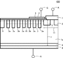
図1および図2は、この発明の実施の形態1に係る半導体装置100の構成図であり、図1(a)は要部平面図、図1(b)は図1(a)のX−X線で切断した要部断面図、図2は図1(b)のF部拡大図である。この半導体装置100は電力用ダイオードであり、縦型のダイオード100aである。
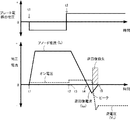
図3および図4は、図1のダイオード100aの動作を説明する図であり、図3(a)はオン状態の図、図3(b)はオフ状態移行時の図、図3(c)はオフ状態の図であり、図4は、図1のダイオード100aの動作波形図である。図3および図4を用いて動作を説明する。
この逆電圧VRの印加により、pアノード領域2とnドリフト領域1aのpn接合からnドリフト領域1aに縦方向と横方向に空乏層17が広がる。横方向に広がった空乏層17aはpガードリング領域3を構成するp+領域3aに達すると、p+領域3aを跳び越して次々と横方向へ広がる。このように、横方向に伸びた空乏層17aの幅は広くなるため、表面での電界強度は小さくなり、表面での耐圧は安定して維持される。
1a nドリフト領域
2 pアノード領域
3 pガードリング領域
3a p+領域
4 絶縁膜
5 プレート電極
6 nカソード領域
7 アノード電極
8 カソード電極
9 チャネルストッパー領域
11 活性領域
12 反転層
13 正孔
14 電子
15 通電領域
16 耐圧構造
17 空乏層
17a 横方向に広がる空乏層
18 ショットキー接合
100,200,300,400 半導体装置
100a 本発明のダイオード(電力用ダイオード)
500 従来のダイオード(電力用ダイオード)
A アノード端子
K カソード端子
G プレート端子
IA アノード電流
IAF 順電流
IAR 逆電流
IRR 逆回復電流
VR 逆電圧
GND グランド電位
Claims (4)
- 第1導電型の半導体基板の表面層に配置される第2導電型の第1半導体領域と、該第1半導体領域を取り囲んで配置される耐圧構造である第2導電型のガードリング領域と、前記第1半導体領域の端部上から前記ガードリング領域に延在する絶縁膜と、前記第1半導体領域の端部と前記ガードリング領域の端部間に挟まれた前記半導体基板上と前記ガードリング領域上に前記絶縁膜を介して配置される導電膜と、前記第1半導体領域上に配置され、前記導電膜と離して配置される主電極と、を備え、
オン時に半導体基板の表面層に反転層が形成される電圧を前記導電膜に印加し、オフ時に前記反転層が消滅する電圧を前記導電膜に印加することを特徴とする半導体装置。 - 前記ガードリング領域が複数で高濃度の第2導電型の第2半導体領域からなり、前記導電膜がリング状に分割され、該分割されたリング状の導電膜が前記第1半導体領域と前記ガードリング領域の間に挟まれた前記半導体基板上、隣接する前記第2半導体領域の間に挟まれた前記半導体基板上の前記絶縁膜を介してそれぞれ配置されることを特徴とする請求項1に記載の半導体装置。
- 前記半導体基板の一部が前記主電極とショットキー接合を形成することを特徴とする請求項1または2に記載の半導体装置。
- 前記半導体基板がn型半導体基板であり、前記第1半導体領域がp型アノード領域であり、前記ガードリング領域がp型ガードリング領域であり、前記第2半導体領域が高濃度のp型領域であり、前記導電膜がプレート電極であることを特徴とする請求項1〜3のいずれか一項に記載の半導体装置。
Priority Applications (2)
| Application Number | Priority Date | Filing Date | Title |
|---|---|---|---|
| JP2013015971A JP6089733B2 (ja) | 2013-01-30 | 2013-01-30 | 半導体装置 |
| US14/154,778 US9443942B2 (en) | 2013-01-30 | 2014-01-14 | Semiconductor device |
Applications Claiming Priority (1)
| Application Number | Priority Date | Filing Date | Title |
|---|---|---|---|
| JP2013015971A JP6089733B2 (ja) | 2013-01-30 | 2013-01-30 | 半導体装置 |
Publications (2)
| Publication Number | Publication Date |
|---|---|
| JP2014146765A JP2014146765A (ja) | 2014-08-14 |
| JP6089733B2 true JP6089733B2 (ja) | 2017-03-08 |
Family
ID=51222015
Family Applications (1)
| Application Number | Title | Priority Date | Filing Date |
|---|---|---|---|
| JP2013015971A Expired - Fee Related JP6089733B2 (ja) | 2013-01-30 | 2013-01-30 | 半導体装置 |
Country Status (2)
| Country | Link |
|---|---|
| US (1) | US9443942B2 (ja) |
| JP (1) | JP6089733B2 (ja) |
Families Citing this family (3)
| Publication number | Priority date | Publication date | Assignee | Title |
|---|---|---|---|---|
| JP2015032627A (ja) * | 2013-07-31 | 2015-02-16 | 株式会社東芝 | 半導体装置 |
| DE102016207117A1 (de) * | 2016-04-27 | 2017-11-02 | Robert Bosch Gmbh | Leistungshalbleiterbauelement und Verfahren zur Herstellung des Leistungshalbleiterbauelements |
| US10784382B2 (en) * | 2017-10-11 | 2020-09-22 | Duet Microelectronics Inc. | Isolation PIN diode structure |
Family Cites Families (17)
| Publication number | Priority date | Publication date | Assignee | Title |
|---|---|---|---|---|
| US4009483A (en) * | 1974-04-04 | 1977-02-22 | Motorola, Inc. | Implementation of surface sensitive semiconductor devices |
| JPS57160159A (en) * | 1981-03-28 | 1982-10-02 | Toshiba Corp | High breakdown voltage planar type semiconductor device |
| JPH04127540A (ja) * | 1990-09-19 | 1992-04-28 | Nec Corp | 絶縁ゲート電界効果トランジスタ |
| US5477077A (en) | 1992-04-17 | 1995-12-19 | Fuji Electric Co., Ltd. | Semiconductor device and a method for the manufacture thereof |
| JP3232763B2 (ja) | 1992-04-17 | 2001-11-26 | 富士電機株式会社 | 半導体装置、およびその駆動方法 |
| JP2812093B2 (ja) * | 1992-09-17 | 1998-10-15 | 株式会社日立製作所 | プレーナ接合を有する半導体装置 |
| JP3417013B2 (ja) * | 1993-10-18 | 2003-06-16 | 株式会社デンソー | 絶縁ゲート型バイポーラトランジスタ |
| JP4054155B2 (ja) * | 2000-02-01 | 2008-02-27 | 三菱電機株式会社 | 半導体装置 |
| KR100535062B1 (ko) * | 2001-06-04 | 2005-12-07 | 마츠시타 덴끼 산교 가부시키가이샤 | 고내압 반도체장치 |
| JP2003347547A (ja) * | 2002-05-27 | 2003-12-05 | Mitsubishi Electric Corp | 電力用半導体装置及びその製造方法 |
| JP4469584B2 (ja) * | 2003-09-12 | 2010-05-26 | 株式会社東芝 | 半導体装置 |
| JP4189415B2 (ja) * | 2006-06-30 | 2008-12-03 | 株式会社東芝 | 半導体装置 |
| JP2008251772A (ja) * | 2007-03-30 | 2008-10-16 | Toshiba Corp | 半導体装置 |
| JP5381420B2 (ja) * | 2008-07-22 | 2014-01-08 | 富士電機株式会社 | 半導体装置 |
| JP5224289B2 (ja) * | 2009-05-12 | 2013-07-03 | 三菱電機株式会社 | 半導体装置 |
| US9117739B2 (en) * | 2010-03-08 | 2015-08-25 | Cree, Inc. | Semiconductor devices with heterojunction barrier regions and methods of fabricating same |
| US9202940B2 (en) * | 2011-09-28 | 2015-12-01 | Mitsubishi Electric Corporation | Semiconductor device |
-
2013
- 2013-01-30 JP JP2013015971A patent/JP6089733B2/ja not_active Expired - Fee Related
-
2014
- 2014-01-14 US US14/154,778 patent/US9443942B2/en not_active Expired - Fee Related
Also Published As
| Publication number | Publication date |
|---|---|
| US20140210037A1 (en) | 2014-07-31 |
| US9443942B2 (en) | 2016-09-13 |
| JP2014146765A (ja) | 2014-08-14 |
Similar Documents
| Publication | Publication Date | Title |
|---|---|---|
| JP5940235B1 (ja) | 半導体装置 | |
| US9362393B2 (en) | Vertical semiconductor device including element active portion and voltage withstanding structure portion, and method of manufacturing the vertical semiconductor device | |
| JP5787853B2 (ja) | 電力用半導体装置 | |
| US7755138B2 (en) | Semiconductor device | |
| US9276137B2 (en) | Diode and semiconductor device including built-in diode | |
| JP5922886B2 (ja) | ダイオードおよび半導体装置 | |
| US8816355B2 (en) | Semiconductor device | |
| JP6641983B2 (ja) | 半導体装置 | |
| US20160141400A1 (en) | Semiconductor device | |
| US20160079369A1 (en) | Semiconductor device | |
| US8912632B2 (en) | Semiconductor device | |
| JP5753814B2 (ja) | ダイオード、半導体装置およびmosfet | |
| US9437727B2 (en) | Semiconductor element including active region, low resistance layer and vertical drift portion | |
| US9059329B2 (en) | Power device with integrated Schottky diode and method for making the same | |
| JP2019054070A (ja) | 半導体装置 | |
| JP2013051345A (ja) | ダイオード、半導体装置およびmosfet | |
| TW201537750A (zh) | 半導體裝置 | |
| TWI788726B (zh) | 半導體裝置 | |
| JP6077309B2 (ja) | ダイオード及びダイオードを内蔵した半導体装置 | |
| JP6089733B2 (ja) | 半導体装置 | |
| US10950723B2 (en) | Semiconductor device and circuit having the same | |
| JPWO2016114138A1 (ja) | 半導体装置 | |
| JP4764998B2 (ja) | 半導体装置 | |
| JP7294004B2 (ja) | 半導体装置 | |
| KR20150076717A (ko) | 전력 반도체 소자 |
Legal Events
| Date | Code | Title | Description |
|---|---|---|---|
| RD02 | Notification of acceptance of power of attorney |
Free format text: JAPANESE INTERMEDIATE CODE: A7422 Effective date: 20151005 |
|
| RD04 | Notification of resignation of power of attorney |
Free format text: JAPANESE INTERMEDIATE CODE: A7424 Effective date: 20151005 |
|
| A621 | Written request for application examination |
Free format text: JAPANESE INTERMEDIATE CODE: A621 Effective date: 20151116 |
|
| A131 | Notification of reasons for refusal |
Free format text: JAPANESE INTERMEDIATE CODE: A131 Effective date: 20161018 |
|
| A977 | Report on retrieval |
Free format text: JAPANESE INTERMEDIATE CODE: A971007 Effective date: 20161020 |
|
| A521 | Request for written amendment filed |
Free format text: JAPANESE INTERMEDIATE CODE: A523 Effective date: 20161121 |
|
| TRDD | Decision of grant or rejection written | ||
| A01 | Written decision to grant a patent or to grant a registration (utility model) |
Free format text: JAPANESE INTERMEDIATE CODE: A01 Effective date: 20170110 |
|
| A61 | First payment of annual fees (during grant procedure) |
Free format text: JAPANESE INTERMEDIATE CODE: A61 Effective date: 20170123 |
|
| R150 | Certificate of patent or registration of utility model |
Ref document number: 6089733 Country of ref document: JP Free format text: JAPANESE INTERMEDIATE CODE: R150 |
|
| R250 | Receipt of annual fees |
Free format text: JAPANESE INTERMEDIATE CODE: R250 |
|
| R250 | Receipt of annual fees |
Free format text: JAPANESE INTERMEDIATE CODE: R250 |
|
| LAPS | Cancellation because of no payment of annual fees |