JP6515515B2 - 発光装置の製造法 - Google Patents
発光装置の製造法 Download PDFInfo
- Publication number
- JP6515515B2 JP6515515B2 JP2014251332A JP2014251332A JP6515515B2 JP 6515515 B2 JP6515515 B2 JP 6515515B2 JP 2014251332 A JP2014251332 A JP 2014251332A JP 2014251332 A JP2014251332 A JP 2014251332A JP 6515515 B2 JP6515515 B2 JP 6515515B2
- Authority
- JP
- Japan
- Prior art keywords
- light emitting
- light
- emitting device
- wavelength conversion
- conversion plate
- Prior art date
- Legal status (The legal status is an assumption and is not a legal conclusion. Google has not performed a legal analysis and makes no representation as to the accuracy of the status listed.)
- Active
Links
Images






Classifications
-
- H—ELECTRICITY
- H10—SEMICONDUCTOR DEVICES; ELECTRIC SOLID-STATE DEVICES NOT OTHERWISE PROVIDED FOR
- H10W—GENERIC PACKAGES, INTERCONNECTIONS, CONNECTORS OR OTHER CONSTRUCTIONAL DETAILS OF DEVICES COVERED BY CLASS H10
- H10W70/00—Package substrates; Interposers; Redistribution layers [RDL]
- H10W70/01—Manufacture or treatment
- H10W70/05—Manufacture or treatment of insulating or insulated package substrates, or of interposers, or of redistribution layers
- H10W70/08—Manufacture or treatment of insulating or insulated package substrates, or of interposers, or of redistribution layers by depositing layers on the chip or wafer, e.g. "chip-first" RDLs
- H10W70/09—Manufacture or treatment of insulating or insulated package substrates, or of interposers, or of redistribution layers by depositing layers on the chip or wafer, e.g. "chip-first" RDLs extending onto an encapsulation that laterally surrounds the chip or wafer, e.g. fan-out wafer level package [FOWLP] RDLs
-
- H—ELECTRICITY
- H10—SEMICONDUCTOR DEVICES; ELECTRIC SOLID-STATE DEVICES NOT OTHERWISE PROVIDED FOR
- H10W—GENERIC PACKAGES, INTERCONNECTIONS, CONNECTORS OR OTHER CONSTRUCTIONAL DETAILS OF DEVICES COVERED BY CLASS H10
- H10W72/00—Interconnections or connectors in packages
- H10W72/90—Bond pads, in general
- H10W72/941—Dispositions of bond pads
- H10W72/9413—Dispositions of bond pads on encapsulations
-
- H—ELECTRICITY
- H10—SEMICONDUCTOR DEVICES; ELECTRIC SOLID-STATE DEVICES NOT OTHERWISE PROVIDED FOR
- H10W—GENERIC PACKAGES, INTERCONNECTIONS, CONNECTORS OR OTHER CONSTRUCTIONAL DETAILS OF DEVICES COVERED BY CLASS H10
- H10W74/00—Encapsulations, e.g. protective coatings
- H10W74/01—Manufacture or treatment
- H10W74/019—Manufacture or treatment using temporary auxiliary substrates
-
- H—ELECTRICITY
- H10—SEMICONDUCTOR DEVICES; ELECTRIC SOLID-STATE DEVICES NOT OTHERWISE PROVIDED FOR
- H10W—GENERIC PACKAGES, INTERCONNECTIONS, CONNECTORS OR OTHER CONSTRUCTIONAL DETAILS OF DEVICES COVERED BY CLASS H10
- H10W74/00—Encapsulations, e.g. protective coatings
- H10W74/10—Encapsulations, e.g. protective coatings characterised by their shape or disposition
- H10W74/131—Encapsulations, e.g. protective coatings characterised by their shape or disposition the semiconductor body being only partially enclosed
- H10W74/142—Encapsulations, e.g. protective coatings characterised by their shape or disposition the semiconductor body being only partially enclosed the encapsulations exposing the passive side of the semiconductor body
Landscapes
- Led Device Packages (AREA)
Description
(実施形態1)
(波長変換板30)
(光反射性樹脂40)
(発光装置100の製造工程)
(波長選別工程)
(直接接合工程)
(電極形成工程)
(第一個片化工程)
(光反射性樹脂形成工程)
(外部接続用電極形成工程)
(支持体除去工程)
(第二個片化工程)
(実施形態2)
(遮光膜形成工程)
(変形例)
(実施形態3)
(リフレクタ形成工程)
(実施形態4)
(レンズ形成工程)
(実施形態5)
1…第一半導体層
2…第二半導体層
3…活性層
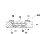
20…パッド電極;20A…第一パッド電極;20B…第二パッド電極
22…外部接続用電極
10…発光素子
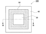
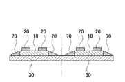
30…波長変換板
40…光反射性樹脂
50…遮光膜
60…サブマウント
70…リフレクタ部
80、80’…レンズ部
1100…半導体素子
1130…波長変換板
1140…光反射性樹脂
SP…支持体
MD、MD’…成形型
Claims (4)
- 複数の発光素子を、前記発光素子の発光を異なる波長の光に変換する板状の波長変換板に、直接接合する接合工程と、
前記波長変換板に直接接合された複数の前記発光素子のそれぞれにおいて、前記波長変換板との接合面の反対側の面に、バンプを加圧により設ける電極形成工程と、
前記波長変換板を切断することにより、発光素子ごとに個片化する第一個片化工程と、
を含み、
前記電極形成工程において、超音波をバンプに印加する発光装置の製造方法。 - 請求項1に記載の発光装置の製造方法であって、さらに、
前記個片化した複数の前記波長変換板を有する発光素子を、前記波長変換板が支持体側となるように支持体上に離間して並べる配置工程と、
前記波長変換板を有する発光素子同士の間に光反射性樹脂を充填して形成する樹脂形成工程と、
前記光反射性樹脂を切断することにより、発光素子ごとに個片化する第二個片化工程と、
を含む発光装置の製造方法。 - 請求項1又は2に記載の発光装置の製造方法であって、
前記直接接合が、表面活性化結合、水酸基結合、原子拡散結合のいずれかである発光装置の製造方法。 - 請求項1〜3のいずれか一に記載の発光装置の製造方法であって、さらに、
前記電極形成工程において、加熱する発光装置の製造方法。
Priority Applications (1)
| Application Number | Priority Date | Filing Date | Title |
|---|---|---|---|
| JP2014251332A JP6515515B2 (ja) | 2014-12-11 | 2014-12-11 | 発光装置の製造法 |
Applications Claiming Priority (1)
| Application Number | Priority Date | Filing Date | Title |
|---|---|---|---|
| JP2014251332A JP6515515B2 (ja) | 2014-12-11 | 2014-12-11 | 発光装置の製造法 |
Publications (2)
| Publication Number | Publication Date |
|---|---|
| JP2016115729A JP2016115729A (ja) | 2016-06-23 |
| JP6515515B2 true JP6515515B2 (ja) | 2019-05-22 |
Family
ID=56142285
Family Applications (1)
| Application Number | Title | Priority Date | Filing Date |
|---|---|---|---|
| JP2014251332A Active JP6515515B2 (ja) | 2014-12-11 | 2014-12-11 | 発光装置の製造法 |
Country Status (1)
| Country | Link |
|---|---|
| JP (1) | JP6515515B2 (ja) |
Families Citing this family (34)
| Publication number | Priority date | Publication date | Assignee | Title |
|---|---|---|---|---|
| JP6380590B2 (ja) * | 2016-06-30 | 2018-08-29 | 日亜化学工業株式会社 | Ledモジュール |
| US10641437B2 (en) | 2016-06-30 | 2020-05-05 | Nichia Corporation | LED module |
| CN106058020A (zh) * | 2016-07-08 | 2016-10-26 | 深圳市兆驰节能照明股份有限公司 | 碗状结构芯片级封装发光装置及其制造方法 |
| JP6724634B2 (ja) * | 2016-07-28 | 2020-07-15 | 日亜化学工業株式会社 | 発光装置の製造方法 |
| JP6504221B2 (ja) * | 2016-09-29 | 2019-04-24 | 日亜化学工業株式会社 | 発光装置の製造方法 |
| JP6512201B2 (ja) | 2016-09-30 | 2019-05-15 | 日亜化学工業株式会社 | 線状発光装置の製造方法及び線状発光装置 |
| JP6955135B2 (ja) | 2016-10-19 | 2021-10-27 | 日亜化学工業株式会社 | 発光装置およびその製造方法 |
| TWI713239B (zh) * | 2016-12-01 | 2020-12-11 | 晶元光電股份有限公司 | 發光裝置 |
| JP6809203B2 (ja) | 2016-12-20 | 2021-01-06 | 日亜化学工業株式会社 | 発光装置の製造方法 |
| KR102730359B1 (ko) * | 2017-01-25 | 2024-11-18 | 엘지이노텍 주식회사 | 광원 모듈 및 이를 구비한 조명 장치 |
| JP7046493B2 (ja) * | 2017-03-07 | 2022-04-04 | スタンレー電気株式会社 | 半導体発光装置及び半導体発光装置の製造方法 |
| WO2018173913A1 (ja) * | 2017-03-21 | 2018-09-27 | 日本特殊陶業株式会社 | 発光装置 |
| JP6579141B2 (ja) * | 2017-03-24 | 2019-09-25 | 日亜化学工業株式会社 | 発光装置および発光装置の製造方法 |
| DE102017109485A1 (de) * | 2017-05-03 | 2018-11-08 | Osram Opto Semiconductors Gmbh | Optoelektronischer Halbleiterchip und Verfahren zur Herstellung eines optoelektronischen Halbleiterchips |
| JP6854715B2 (ja) | 2017-06-30 | 2021-04-07 | 日亜化学工業株式会社 | 発光装置の製造方法 |
| JP6766795B2 (ja) * | 2017-06-30 | 2020-10-14 | 日亜化学工業株式会社 | 発光モジュールの製造方法及び発光モジュール |
| JP6928244B2 (ja) | 2017-08-22 | 2021-09-01 | 日亜化学工業株式会社 | 発光装置 |
| JP7082270B2 (ja) | 2017-08-28 | 2022-06-08 | 日亜化学工業株式会社 | 発光装置 |
| JP6665872B2 (ja) * | 2018-01-15 | 2020-03-13 | 日亜化学工業株式会社 | 発光装置及び発光装置の製造方法 |
| DE102018101424A1 (de) * | 2018-01-23 | 2019-07-25 | Osram Opto Semiconductors Gmbh | Licht emittierendes bauelement und verfahren zur herstellung eines licht emittierenden bauelements |
| JPWO2019150747A1 (ja) * | 2018-01-30 | 2021-02-04 | パナソニックIpマネジメント株式会社 | 蛍光体およびその製造方法 |
| KR102567568B1 (ko) * | 2018-04-06 | 2023-08-16 | 쑤저우 레킨 세미컨덕터 컴퍼니 리미티드 | 반도체 소자 패키지 |
| JP6912730B2 (ja) * | 2018-07-09 | 2021-08-04 | 日亜化学工業株式会社 | 発光モジュールの製造方法 |
| KR102675863B1 (ko) * | 2019-01-29 | 2024-06-17 | 삼성전자주식회사 | 발광 소자 패키지 및 이의 제조 방법 |
| CN111490134B (zh) * | 2019-01-29 | 2024-12-03 | 日亚化学工业株式会社 | 发光装置的制造方法 |
| JP7223938B2 (ja) * | 2019-02-12 | 2023-02-17 | 日亜化学工業株式会社 | 発光装置の製造方法 |
| JP2020164678A (ja) | 2019-03-29 | 2020-10-08 | 日亜化学工業株式会社 | シリコーン樹脂組成物及びその製造方法 |
| JP6849139B1 (ja) * | 2019-08-02 | 2021-03-24 | 日亜化学工業株式会社 | 発光装置および面発光光源 |
| KR102203649B1 (ko) * | 2019-09-10 | 2021-01-15 | (주)라이타이저 | 서브 픽셀 csp, 서브 픽셀 csp의 제조 방법, 디스플레이 장치의 제조 방법 및 그 방법에 의해 제조되는 디스플레이 장치 |
| US11398592B2 (en) | 2019-09-25 | 2022-07-26 | Nichia Corporation | Method for manufacturing light emitting module and light emitting module |
| JP7116330B2 (ja) * | 2020-01-31 | 2022-08-10 | 日亜化学工業株式会社 | 発光装置の製造方法 |
| JP7386417B2 (ja) * | 2020-03-18 | 2023-11-27 | 日亜化学工業株式会社 | 発光装置及びその製造方法 |
| JP7054020B2 (ja) * | 2020-04-28 | 2022-04-13 | 日亜化学工業株式会社 | 発光装置 |
| JP7845368B2 (ja) * | 2021-07-30 | 2026-04-14 | ソニーグループ株式会社 | 発光装置及び画像表示装置 |
Family Cites Families (15)
| Publication number | Priority date | Publication date | Assignee | Title |
|---|---|---|---|---|
| EP1959506A2 (en) * | 1997-01-31 | 2008-08-20 | Matsushita Electric Industrial Co., Ltd. | Method of manufacturing a semiconductor light-emitting device |
| JP3869562B2 (ja) * | 1998-10-16 | 2007-01-17 | 三洋電機株式会社 | 半導体装置の製造方法 |
| JP2002118137A (ja) * | 2000-07-31 | 2002-04-19 | Nichia Chem Ind Ltd | 半導体発光素子チップとそのバンプ形成方法及びその半導体発光素子チップを用いたディスプレイとセグメント表示部 |
| JP4516378B2 (ja) * | 2004-08-13 | 2010-08-04 | ローム株式会社 | 半導体発光装置 |
| JP4162094B2 (ja) * | 2006-05-30 | 2008-10-08 | 三菱重工業株式会社 | 常温接合によるデバイス、デバイス製造方法ならびに常温接合装置 |
| JP5366674B2 (ja) * | 2008-06-27 | 2013-12-11 | パナソニック株式会社 | 実装構造体および実装方法 |
| JP5567657B2 (ja) * | 2009-04-01 | 2014-08-06 | クリック アンド ソッファ インダストリーズ、インク. | 導電性バンプまたはワイヤループを形成する方法 |
| US8597963B2 (en) * | 2009-05-19 | 2013-12-03 | Intematix Corporation | Manufacture of light emitting devices with phosphor wavelength conversion |
| JP2011166617A (ja) * | 2010-02-12 | 2011-08-25 | Seiko Instruments Inc | 圧電振動子の製造方法、圧電振動子、発振器、電子機器および電波時計 |
| CN102823000B (zh) * | 2010-04-08 | 2016-08-03 | 日亚化学工业株式会社 | 发光装置及其制造方法 |
| JP2013003491A (ja) * | 2011-06-21 | 2013-01-07 | Seiko Epson Corp | 偏光変換素子、偏光変換ユニット及び投射装置 |
| JP6094062B2 (ja) * | 2012-06-01 | 2017-03-15 | 日亜化学工業株式会社 | 発光装置及びその製造方法 |
| JP6139071B2 (ja) * | 2012-07-30 | 2017-05-31 | 日亜化学工業株式会社 | 発光装置とその製造方法 |
| JP2014103262A (ja) * | 2012-11-20 | 2014-06-05 | Nichia Chem Ind Ltd | 発光装置の製造方法、実装基板および発光装置 |
| JP6067408B2 (ja) * | 2013-02-20 | 2017-01-25 | スタンレー電気株式会社 | フリップチップ型半導体発光素子、半導体装置及びその製造方法 |
-
2014
- 2014-12-11 JP JP2014251332A patent/JP6515515B2/ja active Active
Also Published As
| Publication number | Publication date |
|---|---|
| JP2016115729A (ja) | 2016-06-23 |
Similar Documents
| Publication | Publication Date | Title |
|---|---|---|
| JP6515515B2 (ja) | 発光装置の製造法 | |
| US9269873B2 (en) | Semiconductor light emitting device and method for manufacturing same | |
| TWI594460B (zh) | 具有整合光學元件的led封裝及其製造方法 | |
| JP5995695B2 (ja) | Led装置の製造方法 | |
| US8490431B2 (en) | Optical device and method for making the same | |
| TWI481070B (zh) | 薄型發光二極體封裝 | |
| CN102800797B (zh) | 具有远离荧光结构的蝙蝠翼透镜 | |
| EP2666193B1 (en) | Led package comprising encapsulation | |
| US20070278513A1 (en) | Semiconductor light emitting device and method of fabricating the same | |
| JP5720759B2 (ja) | 光半導体装置 | |
| JP2014112669A (ja) | 半導体発光装置及びその製造方法 | |
| US10461227B2 (en) | Method for manufacturing light emitting device, and light emitting device | |
| JP2007073825A (ja) | 半導体発光装置 | |
| CN104396035B (zh) | 通过透明间隔物从led分离的磷光体 | |
| JP2007207921A (ja) | 表面実装型光半導体デバイスの製造方法 | |
| WO2013115379A1 (ja) | 半導体発光装置及びその製造方法 | |
| WO2016021476A1 (ja) | 半導体装置及びその製造方法 | |
| WO2011151998A1 (ja) | 発光装置及びその製造方法 | |
| KR101466572B1 (ko) | 변환 엘리먼트를 통한 광전자 반도체 컴포넌트의 접촉 및 대응하는 광전자 반도체 컴포넌트 | |
| JP2019201089A (ja) | チップスケールパッケージング発光素子の斜角チップ反射器およびその製造方法 | |
| JP2011210963A (ja) | 発光装置の製造方法 | |
| JP2015185685A (ja) | 発光装置の製造方法及び照明装置 | |
| US20130065332A1 (en) | Method for manufacturing led with an encapsulant having a flat top face | |
| TW201739071A (zh) | 製造光電組件之方法及光電組件 | |
| KR101460742B1 (ko) | 반도체 소자 구조물을 제조하는 방법 |
Legal Events
| Date | Code | Title | Description |
|---|---|---|---|
| A621 | Written request for application examination |
Free format text: JAPANESE INTERMEDIATE CODE: A621 Effective date: 20170626 |
|
| A131 | Notification of reasons for refusal |
Free format text: JAPANESE INTERMEDIATE CODE: A131 Effective date: 20180619 |
|
| A977 | Report on retrieval |
Free format text: JAPANESE INTERMEDIATE CODE: A971007 Effective date: 20180627 |
|
| A521 | Request for written amendment filed |
Free format text: JAPANESE INTERMEDIATE CODE: A523 Effective date: 20180806 |
|
| A02 | Decision of refusal |
Free format text: JAPANESE INTERMEDIATE CODE: A02 Effective date: 20181009 |
|
| A521 | Request for written amendment filed |
Free format text: JAPANESE INTERMEDIATE CODE: A523 Effective date: 20181226 |
|
| A911 | Transfer to examiner for re-examination before appeal (zenchi) |
Free format text: JAPANESE INTERMEDIATE CODE: A911 Effective date: 20190108 |
|
| TRDD | Decision of grant or rejection written | ||
| A01 | Written decision to grant a patent or to grant a registration (utility model) |
Free format text: JAPANESE INTERMEDIATE CODE: A01 Effective date: 20190319 |
|
| A61 | First payment of annual fees (during grant procedure) |
Free format text: JAPANESE INTERMEDIATE CODE: A61 Effective date: 20190401 |
|
| R150 | Certificate of patent or registration of utility model |
Ref document number: 6515515 Country of ref document: JP Free format text: JAPANESE INTERMEDIATE CODE: R150 |
|
| R250 | Receipt of annual fees |
Free format text: JAPANESE INTERMEDIATE CODE: R250 |
|
| R250 | Receipt of annual fees |
Free format text: JAPANESE INTERMEDIATE CODE: R250 |
|
| R250 | Receipt of annual fees |
Free format text: JAPANESE INTERMEDIATE CODE: R250 |
|
| R250 | Receipt of annual fees |
Free format text: JAPANESE INTERMEDIATE CODE: R250 |