JP6561383B2 - 光変調素子 - Google Patents
光変調素子 Download PDFInfo
- Publication number
- JP6561383B2 JP6561383B2 JP2017069820A JP2017069820A JP6561383B2 JP 6561383 B2 JP6561383 B2 JP 6561383B2 JP 2017069820 A JP2017069820 A JP 2017069820A JP 2017069820 A JP2017069820 A JP 2017069820A JP 6561383 B2 JP6561383 B2 JP 6561383B2
- Authority
- JP
- Japan
- Prior art keywords
- modulation element
- electrode
- light modulation
- substrate
- copper
- Prior art date
- Legal status (The legal status is an assumption and is not a legal conclusion. Google has not performed a legal analysis and makes no representation as to the accuracy of the status listed.)
- Active
Links
Images


Classifications
-
- G—PHYSICS
- G02—OPTICS
- G02F—OPTICAL DEVICES OR ARRANGEMENTS FOR THE CONTROL OF LIGHT BY MODIFICATION OF THE OPTICAL PROPERTIES OF THE MEDIA OF THE ELEMENTS INVOLVED THEREIN; NON-LINEAR OPTICS; FREQUENCY-CHANGING OF LIGHT; OPTICAL LOGIC ELEMENTS; OPTICAL ANALOGUE/DIGITAL CONVERTERS
- G02F1/00—Devices or arrangements for the control of the intensity, colour, phase, polarisation or direction of light arriving from an independent light source, e.g. switching, gating or modulating; Non-linear optics
- G02F1/01—Devices or arrangements for the control of the intensity, colour, phase, polarisation or direction of light arriving from an independent light source, e.g. switching, gating or modulating; Non-linear optics for the control of the intensity, phase, polarisation or colour
- G02F1/21—Devices or arrangements for the control of the intensity, colour, phase, polarisation or direction of light arriving from an independent light source, e.g. switching, gating or modulating; Non-linear optics for the control of the intensity, phase, polarisation or colour by interference
- G02F1/225—Devices or arrangements for the control of the intensity, colour, phase, polarisation or direction of light arriving from an independent light source, e.g. switching, gating or modulating; Non-linear optics for the control of the intensity, phase, polarisation or colour by interference in an optical waveguide structure
- G02F1/2255—Devices or arrangements for the control of the intensity, colour, phase, polarisation or direction of light arriving from an independent light source, e.g. switching, gating or modulating; Non-linear optics for the control of the intensity, phase, polarisation or colour by interference in an optical waveguide structure controlled by a high-frequency electromagnetic component in an electric waveguide structure
-
- G—PHYSICS
- G02—OPTICS
- G02F—OPTICAL DEVICES OR ARRANGEMENTS FOR THE CONTROL OF LIGHT BY MODIFICATION OF THE OPTICAL PROPERTIES OF THE MEDIA OF THE ELEMENTS INVOLVED THEREIN; NON-LINEAR OPTICS; FREQUENCY-CHANGING OF LIGHT; OPTICAL LOGIC ELEMENTS; OPTICAL ANALOGUE/DIGITAL CONVERTERS
- G02F1/00—Devices or arrangements for the control of the intensity, colour, phase, polarisation or direction of light arriving from an independent light source, e.g. switching, gating or modulating; Non-linear optics
- G02F1/01—Devices or arrangements for the control of the intensity, colour, phase, polarisation or direction of light arriving from an independent light source, e.g. switching, gating or modulating; Non-linear optics for the control of the intensity, phase, polarisation or colour
- G02F1/03—Devices or arrangements for the control of the intensity, colour, phase, polarisation or direction of light arriving from an independent light source, e.g. switching, gating or modulating; Non-linear optics for the control of the intensity, phase, polarisation or colour based on ceramics or electro-optical crystals, e.g. exhibiting Pockels effect or Kerr effect
- G02F1/035—Devices or arrangements for the control of the intensity, colour, phase, polarisation or direction of light arriving from an independent light source, e.g. switching, gating or modulating; Non-linear optics for the control of the intensity, phase, polarisation or colour based on ceramics or electro-optical crystals, e.g. exhibiting Pockels effect or Kerr effect in an optical waveguide structure
-
- G—PHYSICS
- G02—OPTICS
- G02F—OPTICAL DEVICES OR ARRANGEMENTS FOR THE CONTROL OF LIGHT BY MODIFICATION OF THE OPTICAL PROPERTIES OF THE MEDIA OF THE ELEMENTS INVOLVED THEREIN; NON-LINEAR OPTICS; FREQUENCY-CHANGING OF LIGHT; OPTICAL LOGIC ELEMENTS; OPTICAL ANALOGUE/DIGITAL CONVERTERS
- G02F1/00—Devices or arrangements for the control of the intensity, colour, phase, polarisation or direction of light arriving from an independent light source, e.g. switching, gating or modulating; Non-linear optics
- G02F1/01—Devices or arrangements for the control of the intensity, colour, phase, polarisation or direction of light arriving from an independent light source, e.g. switching, gating or modulating; Non-linear optics for the control of the intensity, phase, polarisation or colour
- G02F1/21—Devices or arrangements for the control of the intensity, colour, phase, polarisation or direction of light arriving from an independent light source, e.g. switching, gating or modulating; Non-linear optics for the control of the intensity, phase, polarisation or colour by interference
- G02F1/212—Mach-Zehnder type
Landscapes
- Physics & Mathematics (AREA)
- Nonlinear Science (AREA)
- General Physics & Mathematics (AREA)
- Optics & Photonics (AREA)
- Electromagnetism (AREA)
- Chemical & Material Sciences (AREA)
- Engineering & Computer Science (AREA)
- Ceramic Engineering (AREA)
- Crystallography & Structural Chemistry (AREA)
- Optical Modulation, Optical Deflection, Nonlinear Optics, Optical Demodulation, Optical Logic Elements (AREA)
Description
本発明の他の態様によると、前記保護層の少なくとも一部は、前記基板の上に設けられ、前記導電層は、前記基板の上に設けられた前記保護層の前記少なくとも一部の上に設けられる。
本発明の他の態様によると、前記保護層の少なくとも一部は、前記導電層の表面を覆うように設けられている。
本発明の他の態様によると、前記保護層の一部は、前記基板の上に設けられ、前記導電層は、前記保護層の前記一部の上に設けられ、前記保護層の他の一部は、前記導電層の表面を覆うように設けられている。
本発明の他の態様によると、前記保護層は、前記基板の表面のうち前記導電層が設けられない領域の上には設けられていない。
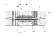
図1は、本発明の一実施形態に係る光変調素子の構成を示す図である。また、図2は、図1に示す光変調素子のAA断面矢視図である。本光変調素子10は、基板100上にマッハツェンダ(MZ、Mach-Zehnder)型光導波路102が配置された、マッハツェンダ型光変調素子である。
〔第1の変形例〕
図3は、図2に示す信号電極108、110及び接地電極112、114、116に代えて用いることのできる信号電極108´、110´及び接地電極112´、114´、116´の構成を示す図である。
図4は、図2に示す信号電極108、110及び接地電極112、114、116に代えて用いることのできる信号電極108´´、110´´及び接地電極112´´、114´´、116´´の構成を示す図である。
Claims (5)
- 基板に設けられた光導波路と、当該光導波路を伝搬する光波を制御する電極と、を備え、当該電極に高周波信号を伝搬させて光変調を行う光変調素子であって、
前記電極は、
銅(Cu)又は銅合金で構成される導電層と、
銅及び銅合金以外の材料で構成される保護層と、
を含み、
前記電極の上部表面の少なくとも一部に、金(Au)で構成される表面層が形成され、
前記保護層は、CuN及び又はCrNで構成される、
光変調素子。 - 前記保護層の少なくとも一部は、前記基板の上に設けられ、前記導電層は、前記基板の上に設けられた前記保護層の前記少なくとも一部の上に設けられる、
請求項1に記載の光変調素子。 - 前記保護層の少なくとも一部は、前記導電層の表面を覆うように設けられている、
請求項1に記載の光変調素子。 - 前記保護層の一部は、前記基板の上に設けられ、前記導電層は、前記保護層の前記一部の上に設けられ、
前記保護層の他の一部は、前記導電層の表面を覆うように設けられている、
請求項1に記載の光変調素子。 - 前記保護層は、前記基板の基板面の領域のうち前記電極が設けられない領域の上には設けられていない、
請求項1ないし4のいずれか一項に記載の光変調素子。
Priority Applications (4)
| Application Number | Priority Date | Filing Date | Title |
|---|---|---|---|
| JP2017069820A JP6561383B2 (ja) | 2017-03-31 | 2017-03-31 | 光変調素子 |
| CN201880010191.6A CN110573941B (zh) | 2017-03-31 | 2018-03-27 | 光调制元件 |
| US16/497,943 US10895765B2 (en) | 2017-03-31 | 2018-03-27 | Optical modulation element |
| PCT/JP2018/012408 WO2018181297A1 (ja) | 2017-03-31 | 2018-03-27 | 光変調素子 |
Applications Claiming Priority (1)
| Application Number | Priority Date | Filing Date | Title |
|---|---|---|---|
| JP2017069820A JP6561383B2 (ja) | 2017-03-31 | 2017-03-31 | 光変調素子 |
Publications (2)
| Publication Number | Publication Date |
|---|---|
| JP2018173454A JP2018173454A (ja) | 2018-11-08 |
| JP6561383B2 true JP6561383B2 (ja) | 2019-08-21 |
Family
ID=63677363
Family Applications (1)
| Application Number | Title | Priority Date | Filing Date |
|---|---|---|---|
| JP2017069820A Active JP6561383B2 (ja) | 2017-03-31 | 2017-03-31 | 光変調素子 |
Country Status (4)
| Country | Link |
|---|---|
| US (1) | US10895765B2 (ja) |
| JP (1) | JP6561383B2 (ja) |
| CN (1) | CN110573941B (ja) |
| WO (1) | WO2018181297A1 (ja) |
Families Citing this family (4)
| Publication number | Priority date | Publication date | Assignee | Title |
|---|---|---|---|---|
| JP2020134875A (ja) * | 2019-02-25 | 2020-08-31 | 富士通オプティカルコンポーネンツ株式会社 | 光変調器 |
| JP2022013232A (ja) * | 2020-07-03 | 2022-01-18 | 富士通オプティカルコンポーネンツ株式会社 | 光デバイス及び光通信装置 |
| JP7505353B2 (ja) * | 2020-09-30 | 2024-06-25 | 住友大阪セメント株式会社 | 光導波路素子、および光変調器 |
| JP7732230B2 (ja) * | 2021-05-28 | 2025-09-02 | 住友大阪セメント株式会社 | 光導波路素子、光変調器、光変調モジュール、及び光送信装置 |
Family Cites Families (24)
| Publication number | Priority date | Publication date | Assignee | Title |
|---|---|---|---|---|
| JPH0713711B2 (ja) | 1987-10-02 | 1995-02-15 | 日本電信電話株式会社 | 高速光変調器 |
| JP2867560B2 (ja) * | 1990-03-02 | 1999-03-08 | 富士通株式会社 | 光導波路デバイス |
| JP3021888B2 (ja) * | 1991-12-04 | 2000-03-15 | 住友金属鉱山株式会社 | 光導波路機能素子及びその製造方法 |
| JP2555942B2 (ja) | 1993-08-27 | 1996-11-20 | 日本電気株式会社 | 光制御デバイス |
| JP2606674B2 (ja) | 1994-10-27 | 1997-05-07 | 日本電気株式会社 | 導波形光デバイス |
| JPH09213730A (ja) * | 1996-02-01 | 1997-08-15 | Matsushita Electron Corp | 高周波用モジュール基板およびそれを用いた高周波電力増幅モジュール |
| JPH09269469A (ja) * | 1996-03-29 | 1997-10-14 | Kyocera Corp | 光導波路デバイス |
| US6198855B1 (en) * | 1996-07-19 | 2001-03-06 | Jds Uniphase Corporation | Velocity-matched, traveling-wave electro-optical devices using non-conductive and conductive polymer buffer layers |
| JP3341588B2 (ja) * | 1996-07-25 | 2002-11-05 | 松下電器産業株式会社 | 高周波集積回路 |
| US5949944A (en) * | 1997-10-02 | 1999-09-07 | Lucent Technologies Inc. | Apparatus and method for dissipating charge from lithium niobate devices |
| JP3179408B2 (ja) * | 1998-04-06 | 2001-06-25 | 日本電気株式会社 | 導波路型光デバイス |
| JP2000323476A (ja) * | 1999-05-12 | 2000-11-24 | Tokyo Electron Ltd | 配線構造およびその製造方法 |
| US6480633B1 (en) * | 1999-06-17 | 2002-11-12 | Agere Systems Inc. | Electro-optic device including a buffer layer of transparent conductive material |
| WO2002097522A1 (fr) * | 2001-05-29 | 2002-12-05 | Hitachi Chemical Co.,Ltd. | Structure d'electrode |
| JP2004219600A (ja) * | 2003-01-14 | 2004-08-05 | Ngk Insulators Ltd | 光変調用電極および光変調器 |
| JP2005091698A (ja) * | 2003-09-17 | 2005-04-07 | Ngk Insulators Ltd | 光変調器 |
| US7418173B2 (en) | 2004-06-30 | 2008-08-26 | Sumitomo Metal Mining Co., Ltd. | Waveguide type optical control element and process for its fabrication |
| US7054054B1 (en) * | 2004-12-20 | 2006-05-30 | Palo Alto Research Center Incorporated | Optical modulator with a traveling surface relief pattern |
| WO2012124830A1 (ja) * | 2011-03-17 | 2012-09-20 | 日本碍子株式会社 | 光変調素子 |
| US9020306B2 (en) * | 2013-03-14 | 2015-04-28 | The Aerospace Corporation | Stable lithium niobate waveguide devices, and methods of making and using same |
| JP6137023B2 (ja) | 2014-03-31 | 2017-05-31 | 住友大阪セメント株式会社 | 光導波路素子 |
| JP6503900B2 (ja) * | 2015-06-01 | 2019-04-24 | 住友大阪セメント株式会社 | 導波路型光素子の駆動方法、及び当該駆動方法に用いる導波路型光素子 |
| JP2017026972A (ja) * | 2015-07-28 | 2017-02-02 | セイコーエプソン株式会社 | 光変調器の製造方法、光変調器および画像表示装置 |
| JP6597698B2 (ja) * | 2017-03-31 | 2019-10-30 | 住友大阪セメント株式会社 | 光変調器 |
-
2017
- 2017-03-31 JP JP2017069820A patent/JP6561383B2/ja active Active
-
2018
- 2018-03-27 WO PCT/JP2018/012408 patent/WO2018181297A1/ja not_active Ceased
- 2018-03-27 CN CN201880010191.6A patent/CN110573941B/zh active Active
- 2018-03-27 US US16/497,943 patent/US10895765B2/en active Active
Also Published As
| Publication number | Publication date |
|---|---|
| US20200026146A1 (en) | 2020-01-23 |
| JP2018173454A (ja) | 2018-11-08 |
| CN110573941B (zh) | 2024-02-20 |
| US10895765B2 (en) | 2021-01-19 |
| CN110573941A (zh) | 2019-12-13 |
| WO2018181297A1 (ja) | 2018-10-04 |
Similar Documents
| Publication | Publication Date | Title |
|---|---|---|
| JP5067464B2 (ja) | 光制御素子 | |
| JP6561383B2 (ja) | 光変調素子 | |
| US10228605B2 (en) | Waveguide optical element | |
| US7643708B2 (en) | Optical modulator | |
| JP5991339B2 (ja) | 光制御素子 | |
| CN108780238B (zh) | 光调制器 | |
| CN107797310B (zh) | 光调制器 | |
| JP4151798B2 (ja) | 光変調器 | |
| JP6327197B2 (ja) | 光変調器 | |
| CN211426971U (zh) | 分布式光强调制器 | |
| CN110824731A (zh) | 分布式光强调制器 | |
| EP4006629B1 (en) | Distributed optical phase modulator | |
| CN107636516B (zh) | 光波导元件 | |
| JP7155848B2 (ja) | 光導波路素子および光変調器 | |
| JP6551449B2 (ja) | 光変調素子 | |
| JP2013210568A (ja) | 光変調器 | |
| JP5075055B2 (ja) | 光変調器 | |
| US20220283453A1 (en) | Distributed light intensity modulator | |
| JP5124382B2 (ja) | 光変調器 | |
| JP6288153B2 (ja) | 光変調器 | |
| JP6394243B2 (ja) | 光導波路素子 | |
| JP2017181633A (ja) | 光変調器 |
Legal Events
| Date | Code | Title | Description |
|---|---|---|---|
| A02 | Decision of refusal |
Free format text: JAPANESE INTERMEDIATE CODE: A02 Effective date: 20181204 |
|
| A521 | Request for written amendment filed |
Free format text: JAPANESE INTERMEDIATE CODE: A523 Effective date: 20190227 |
|
| A911 | Transfer to examiner for re-examination before appeal (zenchi) |
Free format text: JAPANESE INTERMEDIATE CODE: A911 Effective date: 20190312 |
|
| TRDD | Decision of grant or rejection written | ||
| A01 | Written decision to grant a patent or to grant a registration (utility model) |
Free format text: JAPANESE INTERMEDIATE CODE: A01 Effective date: 20190604 |
|
| A61 | First payment of annual fees (during grant procedure) |
Free format text: JAPANESE INTERMEDIATE CODE: A61 Effective date: 20190702 |
|
| A521 | Request for written amendment filed |
Free format text: JAPANESE INTERMEDIATE CODE: A821 Effective date: 20190702 |
|
| R150 | Certificate of patent or registration of utility model |
Ref document number: 6561383 Country of ref document: JP Free format text: JAPANESE INTERMEDIATE CODE: R150 |
|
| R250 | Receipt of annual fees |
Free format text: JAPANESE INTERMEDIATE CODE: R250 |
|
| R250 | Receipt of annual fees |
Free format text: JAPANESE INTERMEDIATE CODE: R250 |
|
| R250 | Receipt of annual fees |
Free format text: JAPANESE INTERMEDIATE CODE: R250 |
|
| R250 | Receipt of annual fees |
Free format text: JAPANESE INTERMEDIATE CODE: R250 |