JP7140610B2 - プラズマ処理装置 - Google Patents
プラズマ処理装置 Download PDFInfo
- Publication number
- JP7140610B2 JP7140610B2 JP2018166773A JP2018166773A JP7140610B2 JP 7140610 B2 JP7140610 B2 JP 7140610B2 JP 2018166773 A JP2018166773 A JP 2018166773A JP 2018166773 A JP2018166773 A JP 2018166773A JP 7140610 B2 JP7140610 B2 JP 7140610B2
- Authority
- JP
- Japan
- Prior art keywords
- electrode
- plasma processing
- processing apparatus
- frequency power
- ring
- Prior art date
- Legal status (The legal status is an assumption and is not a legal conclusion. Google has not performed a legal analysis and makes no representation as to the accuracy of the status listed.)
- Active
Links
Images


Classifications
-
- H—ELECTRICITY
- H01—ELECTRIC ELEMENTS
- H01J—ELECTRIC DISCHARGE TUBES OR DISCHARGE LAMPS
- H01J37/00—Discharge tubes with provision for introducing objects or material to be exposed to the discharge, e.g. for the purpose of examination or processing thereof
- H01J37/32—Gas-filled discharge tubes
- H01J37/32431—Constructional details of the reactor
- H01J37/32532—Electrodes
- H01J37/3255—Material
-
- H—ELECTRICITY
- H01—ELECTRIC ELEMENTS
- H01J—ELECTRIC DISCHARGE TUBES OR DISCHARGE LAMPS
- H01J37/00—Discharge tubes with provision for introducing objects or material to be exposed to the discharge, e.g. for the purpose of examination or processing thereof
- H01J37/32—Gas-filled discharge tubes
- H01J37/32431—Constructional details of the reactor
- H01J37/32532—Electrodes
-
- H—ELECTRICITY
- H01—ELECTRIC ELEMENTS
- H01J—ELECTRIC DISCHARGE TUBES OR DISCHARGE LAMPS
- H01J37/00—Discharge tubes with provision for introducing objects or material to be exposed to the discharge, e.g. for the purpose of examination or processing thereof
- H01J37/32—Gas-filled discharge tubes
- H01J37/32009—Arrangements for generation of plasma specially adapted for examination or treatment of objects, e.g. plasma sources
- H01J37/32192—Microwave generated discharge
- H01J37/32201—Generating means
-
- C—CHEMISTRY; METALLURGY
- C23—COATING METALLIC MATERIAL; COATING MATERIAL WITH METALLIC MATERIAL; CHEMICAL SURFACE TREATMENT; DIFFUSION TREATMENT OF METALLIC MATERIAL; COATING BY VACUUM EVAPORATION, BY SPUTTERING, BY ION IMPLANTATION OR BY CHEMICAL VAPOUR DEPOSITION, IN GENERAL; INHIBITING CORROSION OF METALLIC MATERIAL OR INCRUSTATION IN GENERAL
- C23C—COATING METALLIC MATERIAL; COATING MATERIAL WITH METALLIC MATERIAL; SURFACE TREATMENT OF METALLIC MATERIAL BY DIFFUSION INTO THE SURFACE, BY CHEMICAL CONVERSION OR SUBSTITUTION; COATING BY VACUUM EVAPORATION, BY SPUTTERING, BY ION IMPLANTATION OR BY CHEMICAL VAPOUR DEPOSITION, IN GENERAL
- C23C14/00—Coating by vacuum evaporation, by sputtering or by ion implantation of the coating forming material
- C23C14/22—Coating by vacuum evaporation, by sputtering or by ion implantation of the coating forming material characterised by the process of coating
- C23C14/50—Substrate holders
-
- C—CHEMISTRY; METALLURGY
- C23—COATING METALLIC MATERIAL; COATING MATERIAL WITH METALLIC MATERIAL; CHEMICAL SURFACE TREATMENT; DIFFUSION TREATMENT OF METALLIC MATERIAL; COATING BY VACUUM EVAPORATION, BY SPUTTERING, BY ION IMPLANTATION OR BY CHEMICAL VAPOUR DEPOSITION, IN GENERAL; INHIBITING CORROSION OF METALLIC MATERIAL OR INCRUSTATION IN GENERAL
- C23C—COATING METALLIC MATERIAL; COATING MATERIAL WITH METALLIC MATERIAL; SURFACE TREATMENT OF METALLIC MATERIAL BY DIFFUSION INTO THE SURFACE, BY CHEMICAL CONVERSION OR SUBSTITUTION; COATING BY VACUUM EVAPORATION, BY SPUTTERING, BY ION IMPLANTATION OR BY CHEMICAL VAPOUR DEPOSITION, IN GENERAL
- C23C16/00—Chemical coating by decomposition of gaseous compounds, without leaving reaction products of surface material in the coating, i.e. chemical vapour deposition [CVD] processes
- C23C16/44—Chemical coating by decomposition of gaseous compounds, without leaving reaction products of surface material in the coating, i.e. chemical vapour deposition [CVD] processes characterised by the method of coating
- C23C16/458—Chemical coating by decomposition of gaseous compounds, without leaving reaction products of surface material in the coating, i.e. chemical vapour deposition [CVD] processes characterised by the method of coating characterised by the method used for supporting substrates in the reaction chamber
- C23C16/4582—Rigid and flat substrates, e.g. plates or discs
- C23C16/4583—Rigid and flat substrates, e.g. plates or discs the substrate being supported substantially horizontally
-
- H—ELECTRICITY
- H01—ELECTRIC ELEMENTS
- H01J—ELECTRIC DISCHARGE TUBES OR DISCHARGE LAMPS
- H01J37/00—Discharge tubes with provision for introducing objects or material to be exposed to the discharge, e.g. for the purpose of examination or processing thereof
- H01J37/32—Gas-filled discharge tubes
- H01J37/32009—Arrangements for generation of plasma specially adapted for examination or treatment of objects, e.g. plasma sources
- H01J37/32082—Radio frequency generated discharge
- H01J37/321—Radio frequency generated discharge the radio frequency energy being inductively coupled to the plasma
- H01J37/32119—Windows
-
- H—ELECTRICITY
- H01—ELECTRIC ELEMENTS
- H01J—ELECTRIC DISCHARGE TUBES OR DISCHARGE LAMPS
- H01J37/00—Discharge tubes with provision for introducing objects or material to be exposed to the discharge, e.g. for the purpose of examination or processing thereof
- H01J37/32—Gas-filled discharge tubes
- H01J37/32009—Arrangements for generation of plasma specially adapted for examination or treatment of objects, e.g. plasma sources
- H01J37/32082—Radio frequency generated discharge
- H01J37/32174—Circuits specially adapted for controlling the RF discharge
-
- H—ELECTRICITY
- H01—ELECTRIC ELEMENTS
- H01J—ELECTRIC DISCHARGE TUBES OR DISCHARGE LAMPS
- H01J37/00—Discharge tubes with provision for introducing objects or material to be exposed to the discharge, e.g. for the purpose of examination or processing thereof
- H01J37/32—Gas-filled discharge tubes
- H01J37/32009—Arrangements for generation of plasma specially adapted for examination or treatment of objects, e.g. plasma sources
- H01J37/32192—Microwave generated discharge
- H01J37/32302—Plural frequencies
-
- H—ELECTRICITY
- H01—ELECTRIC ELEMENTS
- H01J—ELECTRIC DISCHARGE TUBES OR DISCHARGE LAMPS
- H01J37/00—Discharge tubes with provision for introducing objects or material to be exposed to the discharge, e.g. for the purpose of examination or processing thereof
- H01J37/32—Gas-filled discharge tubes
- H01J37/32009—Arrangements for generation of plasma specially adapted for examination or treatment of objects, e.g. plasma sources
- H01J37/32192—Microwave generated discharge
- H01J37/32311—Circuits specially adapted for controlling the microwave discharge
-
- H—ELECTRICITY
- H01—ELECTRIC ELEMENTS
- H01J—ELECTRIC DISCHARGE TUBES OR DISCHARGE LAMPS
- H01J37/00—Discharge tubes with provision for introducing objects or material to be exposed to the discharge, e.g. for the purpose of examination or processing thereof
- H01J37/32—Gas-filled discharge tubes
- H01J37/32431—Constructional details of the reactor
- H01J37/32458—Vessel
- H01J37/32513—Sealing means, e.g. sealing between different parts of the vessel
-
- H—ELECTRICITY
- H01—ELECTRIC ELEMENTS
- H01J—ELECTRIC DISCHARGE TUBES OR DISCHARGE LAMPS
- H01J37/00—Discharge tubes with provision for introducing objects or material to be exposed to the discharge, e.g. for the purpose of examination or processing thereof
- H01J37/32—Gas-filled discharge tubes
- H01J37/32431—Constructional details of the reactor
- H01J37/32532—Electrodes
- H01J37/32568—Relative arrangement or disposition of electrodes; moving means
-
- H—ELECTRICITY
- H01—ELECTRIC ELEMENTS
- H01J—ELECTRIC DISCHARGE TUBES OR DISCHARGE LAMPS
- H01J37/00—Discharge tubes with provision for introducing objects or material to be exposed to the discharge, e.g. for the purpose of examination or processing thereof
- H01J37/32—Gas-filled discharge tubes
- H01J37/32431—Constructional details of the reactor
- H01J37/32623—Mechanical discharge control means
- H01J37/32642—Focus rings
-
- H—ELECTRICITY
- H01—ELECTRIC ELEMENTS
- H01J—ELECTRIC DISCHARGE TUBES OR DISCHARGE LAMPS
- H01J37/00—Discharge tubes with provision for introducing objects or material to be exposed to the discharge, e.g. for the purpose of examination or processing thereof
- H01J37/32—Gas-filled discharge tubes
- H01J37/32431—Constructional details of the reactor
- H01J37/3266—Magnetic control means
-
- H—ELECTRICITY
- H01—ELECTRIC ELEMENTS
- H01J—ELECTRIC DISCHARGE TUBES OR DISCHARGE LAMPS
- H01J37/00—Discharge tubes with provision for introducing objects or material to be exposed to the discharge, e.g. for the purpose of examination or processing thereof
- H01J37/32—Gas-filled discharge tubes
- H01J37/32431—Constructional details of the reactor
- H01J37/32715—Workpiece holder
-
- H—ELECTRICITY
- H01—ELECTRIC ELEMENTS
- H01J—ELECTRIC DISCHARGE TUBES OR DISCHARGE LAMPS
- H01J37/00—Discharge tubes with provision for introducing objects or material to be exposed to the discharge, e.g. for the purpose of examination or processing thereof
- H01J37/32—Gas-filled discharge tubes
- H01J37/32431—Constructional details of the reactor
- H01J37/32798—Further details of plasma apparatus not provided for in groups H01J37/3244 - H01J37/32788; special provisions for cleaning or maintenance of the apparatus
- H01J37/32807—Construction (includes replacing parts of the apparatus)
-
- H—ELECTRICITY
- H10—SEMICONDUCTOR DEVICES; ELECTRIC SOLID-STATE DEVICES NOT OTHERWISE PROVIDED FOR
- H10P—GENERIC PROCESSES OR APPARATUS FOR THE MANUFACTURE OR TREATMENT OF DEVICES COVERED BY CLASS H10
- H10P72/00—Handling or holding of wafers, substrates or devices during manufacture or treatment thereof
- H10P72/04—Apparatus for manufacture or treatment
- H10P72/0402—Apparatus for fluid treatment
- H10P72/0418—Apparatus for fluid treatment for etching
- H10P72/0421—Apparatus for fluid treatment for etching for drying etching
-
- H—ELECTRICITY
- H10—SEMICONDUCTOR DEVICES; ELECTRIC SOLID-STATE DEVICES NOT OTHERWISE PROVIDED FOR
- H10P—GENERIC PROCESSES OR APPARATUS FOR THE MANUFACTURE OR TREATMENT OF DEVICES COVERED BY CLASS H10
- H10P72/00—Handling or holding of wafers, substrates or devices during manufacture or treatment thereof
- H10P72/04—Apparatus for manufacture or treatment
- H10P72/0431—Apparatus for thermal treatment
- H10P72/0434—Apparatus for thermal treatment mainly by convection
-
- H—ELECTRICITY
- H10—SEMICONDUCTOR DEVICES; ELECTRIC SOLID-STATE DEVICES NOT OTHERWISE PROVIDED FOR
- H10P—GENERIC PROCESSES OR APPARATUS FOR THE MANUFACTURE OR TREATMENT OF DEVICES COVERED BY CLASS H10
- H10P72/00—Handling or holding of wafers, substrates or devices during manufacture or treatment thereof
- H10P72/70—Handling or holding of wafers, substrates or devices during manufacture or treatment thereof for supporting or gripping
- H10P72/72—Handling or holding of wafers, substrates or devices during manufacture or treatment thereof for supporting or gripping using electrostatic chucks
- H10P72/722—Details of electrostatic chucks
-
- H—ELECTRICITY
- H10—SEMICONDUCTOR DEVICES; ELECTRIC SOLID-STATE DEVICES NOT OTHERWISE PROVIDED FOR
- H10P—GENERIC PROCESSES OR APPARATUS FOR THE MANUFACTURE OR TREATMENT OF DEVICES COVERED BY CLASS H10
- H10P72/00—Handling or holding of wafers, substrates or devices during manufacture or treatment thereof
- H10P72/70—Handling or holding of wafers, substrates or devices during manufacture or treatment thereof for supporting or gripping
- H10P72/76—Handling or holding of wafers, substrates or devices during manufacture or treatment thereof for supporting or gripping using mechanical means, e.g. clamps or pinches
- H10P72/7604—Handling or holding of wafers, substrates or devices during manufacture or treatment thereof for supporting or gripping using mechanical means, e.g. clamps or pinches the wafers being placed on a susceptor, stage or support
- H10P72/7611—Handling or holding of wafers, substrates or devices during manufacture or treatment thereof for supporting or gripping using mechanical means, e.g. clamps or pinches the wafers being placed on a susceptor, stage or support characterised by edge profile or support profile
-
- H—ELECTRICITY
- H01—ELECTRIC ELEMENTS
- H01J—ELECTRIC DISCHARGE TUBES OR DISCHARGE LAMPS
- H01J2237/00—Discharge tubes exposing object to beam, e.g. for analysis treatment, etching, imaging
- H01J2237/32—Processing objects by plasma generation
- H01J2237/33—Processing objects by plasma generation characterised by the type of processing
- H01J2237/334—Etching
- H01J2237/3343—Problems associated with etching
Landscapes
- Chemical & Material Sciences (AREA)
- Engineering & Computer Science (AREA)
- Physics & Mathematics (AREA)
- Plasma & Fusion (AREA)
- Analytical Chemistry (AREA)
- Materials Engineering (AREA)
- Chemical Kinetics & Catalysis (AREA)
- Mechanical Engineering (AREA)
- Metallurgy (AREA)
- Organic Chemistry (AREA)
- General Chemical & Material Sciences (AREA)
- Drying Of Semiconductors (AREA)
- Plasma Technology (AREA)
- Coating By Spraying Or Casting (AREA)
Description
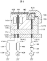
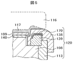
101 真空容器
102 シャワープレート
102a ガス供給部
103 誘電体窓
104 処理室
106 マイクロ波電源
107 磁場発生コイル
107a 磁場発生コイル用電源
108 電極基材
109 試料
110 排気口
111 静電吸着用電極
113 下部サセプタリング
120 ウェハ載置用電極
124 第1の高周波電源
127 第2の高周波電源
138 上部サセプタリング
139 絶縁リング
140 誘電体膜
160 制御部
170 リング電極
171 薄膜電極
172 誘電体膜
Claims (8)
- 真空容器と、
前記真空容器の内部で被処理試料を載置する電極基材と前記電極基材の外周部分を覆う絶縁性の材料で形成されたサセプタリングと前記サセプタリングに覆われて前記電極基材の外周を囲むように配置された絶縁リングであって上面と前記電極基材の外周と対向する内周面の少なくとも一部とにわたってこれらの面の上面を覆う薄膜電極が形成された絶縁リングとを備えた載置台と、
前記載置台の前記電極基材に第1の高周波電力を印加する第1の高周波電力印加部と、
前記絶縁リングに形成された前記薄膜電極に第2の高周波電力を印加する第2の高周波電力印加部と、
前記真空容器の内部で前記載置台の上部にプラズマを発生させるプラズマ発生手段と、
前記第1の高周波電力印加部と前記第2の高周波電力印加部と前記プラズマ発生手段とを制御する制御部と
を備えたことを特徴とするプラズマ処理装置。 - 請求項1記載のプラズマ処理装置であって、前記薄膜電極は、表面を誘電体の膜で覆われていることを特徴とするプラズマ処理装置。
- 請求項2記載のプラズマ処理装置であって、前記薄膜電極はタングステンの膜で形成されており、前記誘電体の膜がアルミナで形成されていることを特徴とするプラズマ処理装置。
- 請求項3記載のプラズマ処理装置であって、前記薄膜電極の前記タングステンの膜は、タングステンを前記絶縁リングの表面に溶射することにより成形されたものであることを特徴とするプラズマ処理装置。
- 請求項3記載のプラズマ処理装置であって、前記薄膜電極の表面を覆う前記アルミナの膜は、前記絶縁リングの前記タングステンの膜が形成された部分を覆ってアルミナを溶射することにより成形されたものであることを特徴とするプラズマ処理装置。
- 請求項1乃至5の何れかに記載のプラズマ処理装置であって、前記絶縁リングの前記薄膜電極が形成された部分のうち前記絶縁リングの上面と前記電極基材の外周と対向する面とが交わる部分は、丸みを帯びた面で接続されていることを特徴とするプラズマ処理装置。
- 請求項1記載のプラズマ処理装置であって、前記載置台は、中央部分に対して周辺部分が凹んだ段差形状を有しており、前記絶縁リングは、前記載置台の周辺部の凹んだ段差形状部分に搭載された状態で前記サセプタリングに覆われていることを特徴とするプラズマ処理装置。
- 請求項1記載のプラズマ処理装置であって、前記プラズマ発生手段は、
前記真空容器の上部に前記載置台と対抗して配置されて誘電体材料で形成された誘電体窓と、
前記真空容器の上部から前記誘電体窓を介して前記真空容器の内部に高周波電力を供給する電力供給部と、
前記真空容器の外部に配置されて前記真空容器の内部に磁界を発生させる磁界発生部と、
を備えていることを特徴とするプラズマ処理装置。
Priority Applications (7)
| Application Number | Priority Date | Filing Date | Title |
|---|---|---|---|
| JP2018166773A JP7140610B2 (ja) | 2018-09-06 | 2018-09-06 | プラズマ処理装置 |
| KR1020190097182A KR102218686B1 (ko) | 2018-09-06 | 2019-08-09 | 플라스마 처리 장치 |
| CN201910746777.5A CN110880443B (zh) | 2018-09-06 | 2019-08-13 | 等离子处理装置 |
| TW110122320A TWI850569B (zh) | 2018-09-06 | 2019-09-03 | 電漿處理裝置 |
| TW108131630A TWI734185B (zh) | 2018-09-06 | 2019-09-03 | 電漿處理裝置 |
| US16/561,785 US20200083026A1 (en) | 2018-09-06 | 2019-09-05 | Plasma processing device |
| JP2022143028A JP7364758B2 (ja) | 2018-09-06 | 2022-09-08 | プラズマ処理方法 |
Applications Claiming Priority (1)
| Application Number | Priority Date | Filing Date | Title |
|---|---|---|---|
| JP2018166773A JP7140610B2 (ja) | 2018-09-06 | 2018-09-06 | プラズマ処理装置 |
Related Child Applications (1)
| Application Number | Title | Priority Date | Filing Date |
|---|---|---|---|
| JP2022143028A Division JP7364758B2 (ja) | 2018-09-06 | 2022-09-08 | プラズマ処理方法 |
Publications (2)
| Publication Number | Publication Date |
|---|---|
| JP2020043100A JP2020043100A (ja) | 2020-03-19 |
| JP7140610B2 true JP7140610B2 (ja) | 2022-09-21 |
Family
ID=69718841
Family Applications (2)
| Application Number | Title | Priority Date | Filing Date |
|---|---|---|---|
| JP2018166773A Active JP7140610B2 (ja) | 2018-09-06 | 2018-09-06 | プラズマ処理装置 |
| JP2022143028A Active JP7364758B2 (ja) | 2018-09-06 | 2022-09-08 | プラズマ処理方法 |
Family Applications After (1)
| Application Number | Title | Priority Date | Filing Date |
|---|---|---|---|
| JP2022143028A Active JP7364758B2 (ja) | 2018-09-06 | 2022-09-08 | プラズマ処理方法 |
Country Status (5)
| Country | Link |
|---|---|
| US (1) | US20200083026A1 (ja) |
| JP (2) | JP7140610B2 (ja) |
| KR (1) | KR102218686B1 (ja) |
| CN (1) | CN110880443B (ja) |
| TW (2) | TWI850569B (ja) |
Families Citing this family (11)
| Publication number | Priority date | Publication date | Assignee | Title |
|---|---|---|---|---|
| WO2020255319A1 (ja) * | 2019-06-20 | 2020-12-24 | 株式会社日立ハイテク | プラズマ処理装置およびプラズマ処理方法 |
| JP7454961B2 (ja) * | 2020-03-05 | 2024-03-25 | 東京エレクトロン株式会社 | プラズマ処理装置 |
| US11906026B2 (en) | 2020-03-06 | 2024-02-20 | C And M Robotics Co., Ltd. | Frictional wave reducer |
| KR102810900B1 (ko) * | 2020-09-08 | 2025-05-22 | 닛폰 하츠죠 가부시키가이샤 | 스테이지 및 그 제조 방법 |
| JP2022049504A (ja) * | 2020-09-16 | 2022-03-29 | 株式会社東芝 | 誘電体バリア放電装置 |
| KR102687065B1 (ko) | 2020-12-29 | 2024-07-24 | 세메스 주식회사 | 기판 처리 장치 및 기판 처리 방법 |
| KR102851225B1 (ko) * | 2021-01-19 | 2025-08-27 | 에스케이하이닉스 주식회사 | 중간 전극을 가진 기판 처리 장치 |
| CN115398602B (zh) * | 2021-03-24 | 2025-02-21 | 株式会社日立高新技术 | 等离子处理装置以及等离子处理方法 |
| CN115206766B (zh) * | 2022-07-28 | 2025-10-10 | 北京北方华创微电子装备有限公司 | 等离子体生成装置、半导体工艺设备及晶圆处理方法 |
| CN120937108A (zh) * | 2023-04-14 | 2025-11-11 | 株式会社普拉斯 | 等离子体处理容器及等离子体处理装置 |
| WO2024215015A2 (ko) * | 2023-04-14 | 2024-10-17 | 주식회사 플라즈맵 | 플라즈마 처리 용기 및 플라즈마 처리 장치 |
Citations (2)
| Publication number | Priority date | Publication date | Assignee | Title |
|---|---|---|---|---|
| JP2011009351A (ja) | 2009-06-24 | 2011-01-13 | Hitachi High-Technologies Corp | プラズマ処理装置およびプラズマ処理方法 |
| JP2017055100A (ja) | 2015-07-13 | 2017-03-16 | ラム リサーチ コーポレーションLam Research Corporation | エッジに限局されたイオン軌道制御及びプラズマ動作を通じた、最端エッジにおけるシース及びウエハのプロフィール調整 |
Family Cites Families (18)
| Publication number | Priority date | Publication date | Assignee | Title |
|---|---|---|---|---|
| JPH05183043A (ja) * | 1992-01-07 | 1993-07-23 | Ryoden Semiconductor Syst Eng Kk | 静電吸着装置及び静電吸着方法 |
| JP2001034372A (ja) * | 1999-07-23 | 2001-02-09 | Alpine Electronics Inc | データ通信方式 |
| JP5165825B2 (ja) * | 2000-01-10 | 2013-03-21 | 東京エレクトロン株式会社 | 分割された電極集合体並びにプラズマ処理方法。 |
| KR100502268B1 (ko) * | 2000-03-01 | 2005-07-22 | 가부시끼가이샤 히다치 세이사꾸쇼 | 플라즈마처리장치 및 방법 |
| JP3606198B2 (ja) * | 2000-12-14 | 2005-01-05 | 株式会社日立製作所 | プラズマ処理装置 |
| CN100418187C (zh) * | 2003-02-07 | 2008-09-10 | 东京毅力科创株式会社 | 等离子体处理装置、环形部件和等离子体处理方法 |
| JP4846190B2 (ja) * | 2003-05-16 | 2011-12-28 | 東京エレクトロン株式会社 | プラズマ処理装置およびその制御方法 |
| JP4365766B2 (ja) * | 2004-10-26 | 2009-11-18 | 京セラ株式会社 | ウェハ支持部材とそれを用いた半導体製造装置 |
| US20080289766A1 (en) * | 2007-05-22 | 2008-11-27 | Samsung Austin Semiconductor Lp | Hot edge ring apparatus and method for increased etch rate uniformity and reduced polymer buildup |
| JP5098882B2 (ja) * | 2007-08-31 | 2012-12-12 | 東京エレクトロン株式会社 | プラズマ処理装置 |
| US8222822B2 (en) * | 2009-10-27 | 2012-07-17 | Tyco Healthcare Group Lp | Inductively-coupled plasma device |
| JP5970268B2 (ja) | 2012-07-06 | 2016-08-17 | 株式会社日立ハイテクノロジーズ | プラズマ処理装置および処理方法 |
| CN103715049B (zh) * | 2012-09-29 | 2016-05-04 | 中微半导体设备(上海)有限公司 | 等离子体处理装置及调节基片边缘区域制程速率的方法 |
| JP6452449B2 (ja) * | 2015-01-06 | 2019-01-16 | 東京エレクトロン株式会社 | 載置台及び基板処理装置 |
| JP6539113B2 (ja) * | 2015-05-28 | 2019-07-03 | 株式会社日立ハイテクノロジーズ | プラズマ処理装置およびプラズマ処理方法 |
| CN108074787A (zh) * | 2016-11-10 | 2018-05-25 | 北京北方华创微电子装备有限公司 | 下电极结构及半导体加工设备 |
| KR102258054B1 (ko) * | 2017-07-24 | 2021-05-28 | 램 리써치 코포레이션 | 이동가능한 에지 링 설계들 |
| CN118380372A (zh) * | 2017-11-21 | 2024-07-23 | 朗姆研究公司 | 底部边缘环和中部边缘环 |
-
2018
- 2018-09-06 JP JP2018166773A patent/JP7140610B2/ja active Active
-
2019
- 2019-08-09 KR KR1020190097182A patent/KR102218686B1/ko active Active
- 2019-08-13 CN CN201910746777.5A patent/CN110880443B/zh active Active
- 2019-09-03 TW TW110122320A patent/TWI850569B/zh active
- 2019-09-03 TW TW108131630A patent/TWI734185B/zh active
- 2019-09-05 US US16/561,785 patent/US20200083026A1/en not_active Abandoned
-
2022
- 2022-09-08 JP JP2022143028A patent/JP7364758B2/ja active Active
Patent Citations (2)
| Publication number | Priority date | Publication date | Assignee | Title |
|---|---|---|---|---|
| JP2011009351A (ja) | 2009-06-24 | 2011-01-13 | Hitachi High-Technologies Corp | プラズマ処理装置およびプラズマ処理方法 |
| JP2017055100A (ja) | 2015-07-13 | 2017-03-16 | ラム リサーチ コーポレーションLam Research Corporation | エッジに限局されたイオン軌道制御及びプラズマ動作を通じた、最端エッジにおけるシース及びウエハのプロフィール調整 |
Also Published As
| Publication number | Publication date |
|---|---|
| JP2022179495A (ja) | 2022-12-02 |
| US20200083026A1 (en) | 2020-03-12 |
| KR102218686B1 (ko) | 2021-02-19 |
| CN110880443B (zh) | 2022-07-08 |
| JP7364758B2 (ja) | 2023-10-18 |
| TW202137393A (zh) | 2021-10-01 |
| KR20200028288A (ko) | 2020-03-16 |
| CN110880443A (zh) | 2020-03-13 |
| TWI850569B (zh) | 2024-08-01 |
| JP2020043100A (ja) | 2020-03-19 |
| TW202011478A (zh) | 2020-03-16 |
| TWI734185B (zh) | 2021-07-21 |
Similar Documents
| Publication | Publication Date | Title |
|---|---|---|
| JP7140610B2 (ja) | プラズマ処理装置 | |
| KR100900585B1 (ko) | 포커스링 및 플라즈마 처리 장치 | |
| JP5554705B2 (ja) | 基材処理のための方法および装置 | |
| JP2001185542A (ja) | プラズマ処理装置及びそれを用いたプラズマ処理方法 | |
| JP2018117024A (ja) | プラズマ処理装置 | |
| JP2016506592A (ja) | 均一なプラズマ密度を有する容量結合プラズマ装置 | |
| TW201833976A (zh) | 雙頻率表面波電漿源 | |
| TWI873545B (zh) | 電漿處理裝置 | |
| KR102876338B1 (ko) | 플라스마 처리 장치 및 플라스마 처리 방법 | |
| JP2019160714A (ja) | プラズマ処理装置 | |
| US10217613B2 (en) | Plasma processing apparatus | |
| KR102207755B1 (ko) | 플라스마 처리 장치 | |
| KR102358480B1 (ko) | 대면적 건식 식각처리 장치 | |
| US20040163595A1 (en) | Plasma processing apparatus | |
| KR20110066686A (ko) | 대면적의 플라즈마를 발생시키는 플라즈마 반응기 | |
| US11664198B2 (en) | Plasma processing apparatus | |
| US12444581B2 (en) | Plasma processing apparatus | |
| CN114496701B (zh) | 等离子体处理装置及其制造方法和等离子体处理方法 | |
| JP4143362B2 (ja) | プラズマ処理装置 | |
| JP2004241592A (ja) | プラズマ処理装置 | |
| KR20240114600A (ko) | 기판 처리 장치 | |
| KR20240126518A (ko) | 기판 처리 장치 |
Legal Events
| Date | Code | Title | Description |
|---|---|---|---|
| A621 | Written request for application examination |
Free format text: JAPANESE INTERMEDIATE CODE: A621 Effective date: 20210618 |
|
| A977 | Report on retrieval |
Free format text: JAPANESE INTERMEDIATE CODE: A971007 Effective date: 20220324 |
|
| A131 | Notification of reasons for refusal |
Free format text: JAPANESE INTERMEDIATE CODE: A131 Effective date: 20220329 |
|
| A521 | Request for written amendment filed |
Free format text: JAPANESE INTERMEDIATE CODE: A523 Effective date: 20220527 |
|
| TRDD | Decision of grant or rejection written | ||
| A01 | Written decision to grant a patent or to grant a registration (utility model) |
Free format text: JAPANESE INTERMEDIATE CODE: A01 Effective date: 20220809 |
|
| A61 | First payment of annual fees (during grant procedure) |
Free format text: JAPANESE INTERMEDIATE CODE: A61 Effective date: 20220908 |
|
| R150 | Certificate of patent or registration of utility model |
Ref document number: 7140610 Country of ref document: JP Free format text: JAPANESE INTERMEDIATE CODE: R150 |