JP7520501B2 - 半導体素子の分析システム及び方法 - Google Patents
半導体素子の分析システム及び方法 Download PDFInfo
- Publication number
- JP7520501B2 JP7520501B2 JP2019224666A JP2019224666A JP7520501B2 JP 7520501 B2 JP7520501 B2 JP 7520501B2 JP 2019224666 A JP2019224666 A JP 2019224666A JP 2019224666 A JP2019224666 A JP 2019224666A JP 7520501 B2 JP7520501 B2 JP 7520501B2
- Authority
- JP
- Japan
- Prior art keywords
- wafer
- etching
- dimensional
- analysis
- semiconductor device
- Prior art date
- Legal status (The legal status is an assumption and is not a legal conclusion. Google has not performed a legal analysis and makes no representation as to the accuracy of the status listed.)
- Active
Links
Images


Classifications
-
- H—ELECTRICITY
- H10—SEMICONDUCTOR DEVICES; ELECTRIC SOLID-STATE DEVICES NOT OTHERWISE PROVIDED FOR
- H10P—GENERIC PROCESSES OR APPARATUS FOR THE MANUFACTURE OR TREATMENT OF DEVICES COVERED BY CLASS H10
- H10P72/00—Handling or holding of wafers, substrates or devices during manufacture or treatment thereof
- H10P72/06—Apparatus for monitoring, sorting, marking, testing or measuring
- H10P72/0616—Monitoring of warpages, curvatures, damages, defects or the like
-
- G—PHYSICS
- G01—MEASURING; TESTING
- G01B—MEASURING LENGTH, THICKNESS OR SIMILAR LINEAR DIMENSIONS; MEASURING ANGLES; MEASURING AREAS; MEASURING IRREGULARITIES OF SURFACES OR CONTOURS
- G01B11/00—Measuring arrangements characterised by the use of optical techniques
- G01B11/002—Measuring arrangements characterised by the use of optical techniques for measuring two or more coordinates
-
- G—PHYSICS
- G01—MEASURING; TESTING
- G01B—MEASURING LENGTH, THICKNESS OR SIMILAR LINEAR DIMENSIONS; MEASURING ANGLES; MEASURING AREAS; MEASURING IRREGULARITIES OF SURFACES OR CONTOURS
- G01B11/00—Measuring arrangements characterised by the use of optical techniques
- G01B11/24—Measuring arrangements characterised by the use of optical techniques for measuring contours or curvatures
-
- G—PHYSICS
- G01—MEASURING; TESTING
- G01B—MEASURING LENGTH, THICKNESS OR SIMILAR LINEAR DIMENSIONS; MEASURING ANGLES; MEASURING AREAS; MEASURING IRREGULARITIES OF SURFACES OR CONTOURS
- G01B15/00—Measuring arrangements characterised by the use of electromagnetic waves or particle radiation, e.g. by the use of microwaves, X-rays, gamma rays or electrons
- G01B15/04—Measuring arrangements characterised by the use of electromagnetic waves or particle radiation, e.g. by the use of microwaves, X-rays, gamma rays or electrons for measuring contours or curvatures
-
- H—ELECTRICITY
- H10—SEMICONDUCTOR DEVICES; ELECTRIC SOLID-STATE DEVICES NOT OTHERWISE PROVIDED FOR
- H10P—GENERIC PROCESSES OR APPARATUS FOR THE MANUFACTURE OR TREATMENT OF DEVICES COVERED BY CLASS H10
- H10P50/00—Etching of wafers, substrates or parts of devices
-
- H—ELECTRICITY
- H10—SEMICONDUCTOR DEVICES; ELECTRIC SOLID-STATE DEVICES NOT OTHERWISE PROVIDED FOR
- H10P—GENERIC PROCESSES OR APPARATUS FOR THE MANUFACTURE OR TREATMENT OF DEVICES COVERED BY CLASS H10
- H10P52/00—Grinding, lapping or polishing of wafers, substrates or parts of devices
-
- H—ELECTRICITY
- H10—SEMICONDUCTOR DEVICES; ELECTRIC SOLID-STATE DEVICES NOT OTHERWISE PROVIDED FOR
- H10P—GENERIC PROCESSES OR APPARATUS FOR THE MANUFACTURE OR TREATMENT OF DEVICES COVERED BY CLASS H10
- H10P70/00—Cleaning of wafers, substrates or parts of devices
- H10P70/20—Cleaning during device manufacture
-
- H—ELECTRICITY
- H10—SEMICONDUCTOR DEVICES; ELECTRIC SOLID-STATE DEVICES NOT OTHERWISE PROVIDED FOR
- H10P—GENERIC PROCESSES OR APPARATUS FOR THE MANUFACTURE OR TREATMENT OF DEVICES COVERED BY CLASS H10
- H10P72/00—Handling or holding of wafers, substrates or devices during manufacture or treatment thereof
- H10P72/04—Apparatus for manufacture or treatment
- H10P72/0402—Apparatus for fluid treatment
- H10P72/0406—Apparatus for fluid treatment for cleaning followed by drying, rinsing, stripping, blasting or the like
-
- H—ELECTRICITY
- H10—SEMICONDUCTOR DEVICES; ELECTRIC SOLID-STATE DEVICES NOT OTHERWISE PROVIDED FOR
- H10P—GENERIC PROCESSES OR APPARATUS FOR THE MANUFACTURE OR TREATMENT OF DEVICES COVERED BY CLASS H10
- H10P72/00—Handling or holding of wafers, substrates or devices during manufacture or treatment thereof
- H10P72/04—Apparatus for manufacture or treatment
- H10P72/0402—Apparatus for fluid treatment
- H10P72/0418—Apparatus for fluid treatment for etching
- H10P72/0421—Apparatus for fluid treatment for etching for drying etching
-
- H—ELECTRICITY
- H10—SEMICONDUCTOR DEVICES; ELECTRIC SOLID-STATE DEVICES NOT OTHERWISE PROVIDED FOR
- H10P—GENERIC PROCESSES OR APPARATUS FOR THE MANUFACTURE OR TREATMENT OF DEVICES COVERED BY CLASS H10
- H10P72/00—Handling or holding of wafers, substrates or devices during manufacture or treatment thereof
- H10P72/04—Apparatus for manufacture or treatment
- H10P72/0402—Apparatus for fluid treatment
- H10P72/0418—Apparatus for fluid treatment for etching
- H10P72/0422—Apparatus for fluid treatment for etching for wet etching
-
- H—ELECTRICITY
- H10—SEMICONDUCTOR DEVICES; ELECTRIC SOLID-STATE DEVICES NOT OTHERWISE PROVIDED FOR
- H10P—GENERIC PROCESSES OR APPARATUS FOR THE MANUFACTURE OR TREATMENT OF DEVICES COVERED BY CLASS H10
- H10P72/00—Handling or holding of wafers, substrates or devices during manufacture or treatment thereof
- H10P72/04—Apparatus for manufacture or treatment
- H10P72/0428—Apparatus for mechanical treatment or grinding or cutting
-
- H—ELECTRICITY
- H10—SEMICONDUCTOR DEVICES; ELECTRIC SOLID-STATE DEVICES NOT OTHERWISE PROVIDED FOR
- H10P—GENERIC PROCESSES OR APPARATUS FOR THE MANUFACTURE OR TREATMENT OF DEVICES COVERED BY CLASS H10
- H10P72/00—Handling or holding of wafers, substrates or devices during manufacture or treatment thereof
- H10P72/04—Apparatus for manufacture or treatment
- H10P72/0451—Apparatus for manufacturing or treating in a plurality of work-stations
- H10P72/0452—Apparatus for manufacturing or treating in a plurality of work-stations characterised by the layout of the process chambers
- H10P72/0454—Apparatus for manufacturing or treating in a plurality of work-stations characterised by the layout of the process chambers surrounding a central transfer chamber
-
- H—ELECTRICITY
- H10—SEMICONDUCTOR DEVICES; ELECTRIC SOLID-STATE DEVICES NOT OTHERWISE PROVIDED FOR
- H10P—GENERIC PROCESSES OR APPARATUS FOR THE MANUFACTURE OR TREATMENT OF DEVICES COVERED BY CLASS H10
- H10P72/00—Handling or holding of wafers, substrates or devices during manufacture or treatment thereof
- H10P72/04—Apparatus for manufacture or treatment
- H10P72/0451—Apparatus for manufacturing or treating in a plurality of work-stations
- H10P72/0468—Apparatus for manufacturing or treating in a plurality of work-stations comprising a chamber adapted to a particular process
- H10P72/0471—Apparatus for manufacturing or treating in a plurality of work-stations comprising a chamber adapted to a particular process comprising at least one ion or electron beam chamber
-
- H—ELECTRICITY
- H10—SEMICONDUCTOR DEVICES; ELECTRIC SOLID-STATE DEVICES NOT OTHERWISE PROVIDED FOR
- H10P—GENERIC PROCESSES OR APPARATUS FOR THE MANUFACTURE OR TREATMENT OF DEVICES COVERED BY CLASS H10
- H10P74/00—Testing or measuring during manufacture or treatment of wafers, substrates or devices
- H10P74/20—Testing or measuring during manufacture or treatment of wafers, substrates or devices characterised by the properties tested or measured, e.g. structural or electrical properties
- H10P74/203—Structural properties, e.g. testing or measuring thicknesses, line widths, warpage, bond strengths or physical defects
-
- H—ELECTRICITY
- H10—SEMICONDUCTOR DEVICES; ELECTRIC SOLID-STATE DEVICES NOT OTHERWISE PROVIDED FOR
- H10P—GENERIC PROCESSES OR APPARATUS FOR THE MANUFACTURE OR TREATMENT OF DEVICES COVERED BY CLASS H10
- H10P74/00—Testing or measuring during manufacture or treatment of wafers, substrates or devices
- H10P74/23—Testing or measuring during manufacture or treatment of wafers, substrates or devices characterised by multiple measurements, corrections, marking or sorting processes
-
- H—ELECTRICITY
- H10—SEMICONDUCTOR DEVICES; ELECTRIC SOLID-STATE DEVICES NOT OTHERWISE PROVIDED FOR
- H10P—GENERIC PROCESSES OR APPARATUS FOR THE MANUFACTURE OR TREATMENT OF DEVICES COVERED BY CLASS H10
- H10P74/00—Testing or measuring during manufacture or treatment of wafers, substrates or devices
- H10P74/27—Structural arrangements therefor
-
- H—ELECTRICITY
- H10—SEMICONDUCTOR DEVICES; ELECTRIC SOLID-STATE DEVICES NOT OTHERWISE PROVIDED FOR
- H10P—GENERIC PROCESSES OR APPARATUS FOR THE MANUFACTURE OR TREATMENT OF DEVICES COVERED BY CLASS H10
- H10P72/00—Handling or holding of wafers, substrates or devices during manufacture or treatment thereof
- H10P72/06—Apparatus for monitoring, sorting, marking, testing or measuring
Landscapes
- Physics & Mathematics (AREA)
- General Physics & Mathematics (AREA)
- Electromagnetism (AREA)
- Testing Or Measuring Of Semiconductors Or The Like (AREA)
- Analysing Materials By The Use Of Radiation (AREA)
- Engineering & Computer Science (AREA)
- Manufacturing & Machinery (AREA)
- Other Investigation Or Analysis Of Materials By Electrical Means (AREA)
Description
Claims (17)
- 分析対象が存在する深さまで、ウェーハの表面の全面を同一のエッチング速度でエッチングする全面エッチングモジュール;
繰り返しエッチングされた前記ウェーハの表面から2次元構造情報を取得する分析モジュール;及び、
前記分析モジュールから繰り返し獲得した前記2次元構造情報を時系列的に積層処理して、3次元イメージを再構成するコンピュータ装置を含み、
前記分析モジュールは、
前記エッチングされたウェーハの表面の物理的イメージを獲得する第1の分析ユニット;及び、
前記エッチングされたウェーハの表面の電気的イメージを獲得する第2の分析ユニットを含む、半導体素子の分析システム。 - 前記全面エッチングモジュールは、前記ウェーハの表面の全面にイオンビームを照射するミリング装置、CMP(Chemical mechanical polishing)装置、乾式エッチング装置及び湿式エッチング装置から選択される一つである、請求項1に記載の半導体素子の分析システム。
- 前記ミリング装置は、前記ウェーハの全面に対してイオンビームを供給するイオンビーム照射部を含む、請求項2に記載の半導体素子の分析システム。
- 前記分析モジュールは、SEM(Scanning Electron Microscope)装置、PEEM(Photo Electron Emission Microscopy)装置、EDX(Energy Dispersive X-ray analysis)装置、XPS(X-rays Photoelectron Spectroscopy)、SPM(Scanning Probe Microscopy)、AFM(Atomic Force Microscopy)及びSTM(Scanning Tunneling Microscopy)のようにプローブ(probe)を用いた計測/分析装置、ラマン分光器(Raman spectroscopy)、TCAD(Technology Computer Aided Design)又は素子内のオプティック(optic)又は電子(electron)の挙動(behavior)を計算及び演算するシミュレーション技法及び光学計測/検査装備(Optical Metrology/Inspection tool)の少なくとも一つである、請求項1に記載の半導体素子の分析システム。
- 前記第1の分析ユニットはSEM装置を含む、請求項1に記載の半導体素子の分析システム。
- 前記第2の分析ユニットはPEEM装置又はEDX装置を含む、請求項1に記載の半導体素子の分析システム。
- 前記全面エッチングモジュールは、
前記ウェーハを支持するステージ;及び、
前記ウェーハの表面の回路層が同一のエッチング速度でエッチングされるように、前記ウェーハの全面に対してイオンビームを照射するイオンビーム照射部を含む、請求項1に記載の半導体素子の分析システム。 - 前記イオンビーム照射部は、前記ウェーハの口径よりも大きい口径を有する、請求項7に記載の半導体素子の分析システム。
- 前記繰り返し得られた2次元構造情報は2次元イメージを含み、
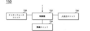
前記コンピュータ装置は、
前記分析モジュールから提供される前記2次元イメージをエッチング深さ及び(X、Y)座標の形態で区分し、前記エッチング深さ及び前記(X、Y)座標値に基づいて、前記2次元イメージを時系列的に積層して前記3次元イメージを再生成する制御器;及び、
前記制御器により区分された2次元イメージを格納する格納ユニットを含む、請求項1に記載の半導体素子の分析システム。 - 前記全面エッチングが進行された前記ウェーハの表面をクリーニングするクリーニングモジュールをさらに含む、請求項1に記載の半導体素子の分析システム。
- 処理する前記ウェーハが待機するロードロックをさらに含み、
前記全面エッチングモジュール、前記分析モジュール及び前記クリーニングモジュールは、前記ロードロックを基準としてクラスター形態で連結する、請求項10に記載の半導体素子の分析システム。 - 前記分析モジュールは、前記ウェーハのエッチング時に発生するエッチング副産物を分析する質量分析器及びOES(Optical Emission Spectroscopy)の少なくとも一つをさらに含む、請求項1に記載の半導体素子の分析システム。
- ウェーハの表面の全体を同一のエッチング速度で設定のエッチングターゲット深さだけ繰り返しエッチングして、前記ウェーハの次の表面を露出させるステップ;
前記エッチングターゲット深さだけ繰り返しエッチングされた前記ウェーハの表面の2次元構造情報を各々獲得するステップ;及び、
繰り返し獲得した前記2次元構造情報を時系列的に積層及び処理して3次元イメージを生成するステップを含み、
前記2次元構造情報を繰り返し獲得するステップは、
前記ウェーハの表面の2次元物理構造情報を獲得するステップ;及び、
前記ウェーハの表面の2次元電気構造情報を獲得するステップを含む、半導体素子の分析方法。 - 前記繰り返し得られた2次元構造情報は2次元イメージを含み、
前記2次元構造情報を繰り返し獲得するステップは、
前記ウェーハのエッチングターゲット深さ別に前記2次元イメージを(X、Y)座標形態で区分するステップ;及び、
前記エッチングターゲット深さ及び前記(X、Y)座標に基づいて、前記繰り返し獲得された2次元イメージを連続積層及び処理するステップを含む、請求項13に記載の半導体素子の分析方法。 - 前記ウェーハの表面のエッチング時に発生するエッチング副産物を分析するステップをさらに含む、請求項13に記載の半導体素子の分析方法。
- 前記エッチング副産物の量を分析して前記エッチングターゲット深さを制御する、請求項15に記載の半導体素子の分析方法。
- 前記ウェーハの表面の全体をエッチングするステップと、前記2次元イメージを測定するステップとの間に、エッチングされた前記ウェーハの表面をクリーニングするステップをさらに含む、請求項14に記載の半導体素子の分析方法。
Applications Claiming Priority (2)
| Application Number | Priority Date | Filing Date | Title |
|---|---|---|---|
| KR1020190088824A KR102705854B1 (ko) | 2019-07-23 | 2019-07-23 | 반도체 소자의 분석 시스템 및 방법 |
| KR10-2019-0088824 | 2019-07-23 |
Publications (2)
| Publication Number | Publication Date |
|---|---|
| JP2021019179A JP2021019179A (ja) | 2021-02-15 |
| JP7520501B2 true JP7520501B2 (ja) | 2024-07-23 |
Family
ID=74189553
Family Applications (1)
| Application Number | Title | Priority Date | Filing Date |
|---|---|---|---|
| JP2019224666A Active JP7520501B2 (ja) | 2019-07-23 | 2019-12-12 | 半導体素子の分析システム及び方法 |
Country Status (4)
| Country | Link |
|---|---|
| US (2) | US11295970B2 (ja) |
| JP (1) | JP7520501B2 (ja) |
| KR (1) | KR102705854B1 (ja) |
| CN (1) | CN112309890B (ja) |
Families Citing this family (6)
| Publication number | Priority date | Publication date | Assignee | Title |
|---|---|---|---|---|
| CN111857111B (zh) * | 2019-04-09 | 2024-07-19 | 商汤集团有限公司 | 对象三维检测及智能驾驶控制方法、装置、介质及设备 |
| TWI786455B (zh) * | 2019-10-30 | 2022-12-11 | 德商卡爾蔡司Smt有限公司 | 確定積體半導體樣本中三維結構間的接觸區域尺寸的方法及其用途、電腦程式產品、以及半導體檢查裝置 |
| CN114646638A (zh) * | 2022-04-12 | 2022-06-21 | 中国电子产品可靠性与环境试验研究所((工业和信息化部电子第五研究所)(中国赛宝实验室)) | 芯片失效分析定位方法、装置、设备及存储介质 |
| CN115900554A (zh) * | 2022-09-08 | 2023-04-04 | 中国电子产品可靠性与环境试验研究所((工业和信息化部电子第五研究所)(中国赛宝实验室)) | 半导体器件的多层铜线路检测方法 |
| TWI894929B (zh) * | 2023-06-19 | 2025-08-21 | 德商卡爾蔡司Smt有限公司 | 在處理實體處執行的方法、含有記憶體及至少一處理器的處理實體、電腦程式及包含該電腦程式的載體 |
| CN120635050A (zh) * | 2025-06-24 | 2025-09-12 | 上海聚跃检测技术有限公司 | 一种基于刻蚀技术的半导体截面结构检测方法及系统 |
Citations (3)
| Publication number | Priority date | Publication date | Assignee | Title |
|---|---|---|---|---|
| JP2004045172A (ja) | 2002-07-11 | 2004-02-12 | Fujitsu Ltd | 3次元構造評価方法 |
| JP2018152330A (ja) | 2017-02-16 | 2018-09-27 | カール ツァイス マイクロスコーピー ゲーエムベーハーCarl Zeiss Microscopy GmbH | 物体を分析する方法およびこの方法を実行するための荷電粒子ビーム装置 |
| JP2019078684A (ja) | 2017-10-26 | 2019-05-23 | 信越半導体株式会社 | シリコンウェーハの金属不純物分析方法 |
Family Cites Families (11)
| Publication number | Priority date | Publication date | Assignee | Title |
|---|---|---|---|---|
| JPH10209112A (ja) * | 1997-01-27 | 1998-08-07 | Tera Tec:Kk | エッチング方法および装置 |
| US6317514B1 (en) | 1998-09-09 | 2001-11-13 | Applied Materials, Inc. | Method and apparatus for inspection of patterned semiconductor wafers |
| WO2003050841A1 (en) | 2001-11-30 | 2003-06-19 | Kla Tencor Corporation | A photoelectron emission microscope for wafer and reticle inspection |
| US9698062B2 (en) * | 2013-02-28 | 2017-07-04 | Veeco Precision Surface Processing Llc | System and method for performing a wet etching process |
| WO2015144700A2 (en) | 2014-03-25 | 2015-10-01 | Carl Zeiss Sms Ltd. | Method and apparatus for generating a predetermined three-dimensional contour of an optical component and/or a wafer |
| KR102257901B1 (ko) | 2014-09-19 | 2021-05-31 | 삼성전자주식회사 | 반도체 검사 장비 및 이를 이용한 반도체 소자의 검사 방법 |
| KR102410666B1 (ko) | 2015-01-09 | 2022-06-20 | 삼성전자주식회사 | 반도체 소자의 계측 방법, 및 이를 이용한 반도체 소자의 제조방법 |
| KR102228497B1 (ko) * | 2016-07-19 | 2021-03-15 | 도쿄엘렉트론가부시키가이샤 | 3 차원 반도체 디바이스 및 그 제조 방법 |
| CN109643725B (zh) * | 2016-08-08 | 2022-07-29 | 东京毅力科创株式会社 | 三维半导体器件及制造方法 |
| US10847376B2 (en) * | 2018-06-28 | 2020-11-24 | Sandisk Technologies Llc | In-situ deposition and etch process and apparatus for precision patterning of semiconductor devices |
| US11018063B2 (en) * | 2018-11-26 | 2021-05-25 | Sandisk Technologies Llc | Method and apparatus for nanoscale-dimension measurement using a diffraction pattern filter |
-
2019
- 2019-07-23 KR KR1020190088824A patent/KR102705854B1/ko active Active
- 2019-10-29 US US16/667,499 patent/US11295970B2/en active Active
- 2019-11-11 CN CN201911094467.6A patent/CN112309890B/zh active Active
- 2019-12-12 JP JP2019224666A patent/JP7520501B2/ja active Active
-
2022
- 2022-02-25 US US17/681,201 patent/US11626306B2/en active Active
Patent Citations (3)
| Publication number | Priority date | Publication date | Assignee | Title |
|---|---|---|---|---|
| JP2004045172A (ja) | 2002-07-11 | 2004-02-12 | Fujitsu Ltd | 3次元構造評価方法 |
| JP2018152330A (ja) | 2017-02-16 | 2018-09-27 | カール ツァイス マイクロスコーピー ゲーエムベーハーCarl Zeiss Microscopy GmbH | 物体を分析する方法およびこの方法を実行するための荷電粒子ビーム装置 |
| JP2019078684A (ja) | 2017-10-26 | 2019-05-23 | 信越半導体株式会社 | シリコンウェーハの金属不純物分析方法 |
Also Published As
| Publication number | Publication date |
|---|---|
| JP2021019179A (ja) | 2021-02-15 |
| US20220277975A1 (en) | 2022-09-01 |
| US20210028033A1 (en) | 2021-01-28 |
| KR102705854B1 (ko) | 2024-09-11 |
| CN112309890A (zh) | 2021-02-02 |
| KR20210011657A (ko) | 2021-02-02 |
| CN112309890B (zh) | 2024-12-10 |
| US11295970B2 (en) | 2022-04-05 |
| US11626306B2 (en) | 2023-04-11 |
Similar Documents
| Publication | Publication Date | Title |
|---|---|---|
| JP7520501B2 (ja) | 半導体素子の分析システム及び方法 | |
| CN115280463B (zh) | 晶片中检查体积的截面成像方法 | |
| Ma et al. | Metrology and diagnostic techniques for nanoelectronics | |
| CN103797351B (zh) | 掠射角铣削 | |
| JP6356397B2 (ja) | 基板の外位置分析システムおよび方法 | |
| CN105264635B (zh) | 用于利用带电粒子束的倾斜或掠射研磨操作的基准设计 | |
| US10101246B2 (en) | Method of preparing a plan-view transmission electron microscope sample used in an integrated circuit analysis | |
| KR102301793B1 (ko) | 이미지 생성 방법 및 이를 수행하기 위한 이미징 시스템 | |
| JP2011522420A (ja) | 集束イオンビームデバイスおよび走査型電子顕微鏡を用いた半導体構造の三次元画像作成方法 | |
| JPWO2020100179A1 (ja) | 画像形成方法及び画像形成システム | |
| US20250231129A1 (en) | E-beam optimization for overlay measurement of buried features | |
| TWI876119B (zh) | 積體電路裝置製造方法與系統 | |
| TW202407336A (zh) | 使用半導體結構的切片和影像斷層成像影像的參數化x射線散射測量 | |
| Bunday et al. | Metrology | |
| Zudhistira et al. | Integration of probing capability into plasma FIB for in-situ Delayering, defect inspection, and EBAC on BEOL defects of sub-20nm FinFET devices | |
| Nowakowski et al. | An innovative technique for large-scale delayering of semiconductor devices with nanometric-scale surface flatness | |
| Maitra et al. | Microstructural investigation and serial section tomography on asic chips for assurance through reverse engineering applications | |
| TWI899942B (zh) | 使用聚焦線測量高度 | |
| TW202609847A (zh) | 對具有降低的銑削製品的埋藏感興趣區域進行3d檢查 | |
| US20260112573A1 (en) | Method and apparatus for charge compensation during 3d tomography | |
| WO2025261786A1 (en) | 3d inspection of buried regions of interest with reduced milling artefacts | |
| Hu et al. | 3D reconstruction and etching profile simulation for wiggling active area effect in dynamic random access memory manufacturing | |
| Narang et al. | Die-Level Roadmap: Post-Isolation Domain | |
| US8384029B2 (en) | Cross-section systems and methods | |
| US20140342477A1 (en) | Method of monitoring semiconductor fabrication process using xps |
Legal Events
| Date | Code | Title | Description |
|---|---|---|---|
| A621 | Written request for application examination |
Free format text: JAPANESE INTERMEDIATE CODE: A621 Effective date: 20221108 |
|
| A977 | Report on retrieval |
Free format text: JAPANESE INTERMEDIATE CODE: A971007 Effective date: 20231218 |
|
| A131 | Notification of reasons for refusal |
Free format text: JAPANESE INTERMEDIATE CODE: A131 Effective date: 20240130 |
|
| A521 | Request for written amendment filed |
Free format text: JAPANESE INTERMEDIATE CODE: A523 Effective date: 20240423 |
|
| TRDD | Decision of grant or rejection written | ||
| A01 | Written decision to grant a patent or to grant a registration (utility model) |
Free format text: JAPANESE INTERMEDIATE CODE: A01 Effective date: 20240625 |
|
| A61 | First payment of annual fees (during grant procedure) |
Free format text: JAPANESE INTERMEDIATE CODE: A61 Effective date: 20240710 |
|
| R150 | Certificate of patent or registration of utility model |
Ref document number: 7520501 Country of ref document: JP Free format text: JAPANESE INTERMEDIATE CODE: R150 |