JP7610040B2 - 電子クリーニング装置 - Google Patents
電子クリーニング装置 Download PDFInfo
- Publication number
- JP7610040B2 JP7610040B2 JP2023568986A JP2023568986A JP7610040B2 JP 7610040 B2 JP7610040 B2 JP 7610040B2 JP 2023568986 A JP2023568986 A JP 2023568986A JP 2023568986 A JP2023568986 A JP 2023568986A JP 7610040 B2 JP7610040 B2 JP 7610040B2
- Authority
- JP
- Japan
- Prior art keywords
- cleaning device
- shielding plate
- sample chamber
- electron source
- secondary electrons
- Prior art date
- Legal status (The legal status is an assumption and is not a legal conclusion. Google has not performed a legal analysis and makes no representation as to the accuracy of the status listed.)
- Active
Links
Images


Classifications
-
- H—ELECTRICITY
- H01—ELECTRIC ELEMENTS
- H01J—ELECTRIC DISCHARGE TUBES OR DISCHARGE LAMPS
- H01J37/00—Discharge tubes with provision for introducing objects or material to be exposed to the discharge, e.g. for the purpose of examination or processing thereof
- H01J37/02—Details
- H01J37/24—Circuit arrangements not adapted to a particular application of the tube and not otherwise provided for
- H01J37/241—High voltage power supply or regulation circuits
-
- H—ELECTRICITY
- H01—ELECTRIC ELEMENTS
- H01J—ELECTRIC DISCHARGE TUBES OR DISCHARGE LAMPS
- H01J37/00—Discharge tubes with provision for introducing objects or material to be exposed to the discharge, e.g. for the purpose of examination or processing thereof
- H01J37/02—Details
- H01J37/04—Arrangements of electrodes and associated parts for generating or controlling the discharge, e.g. electron-optical arrangement or ion-optical arrangement
- H01J37/06—Electron sources; Electron guns
-
- H—ELECTRICITY
- H01—ELECTRIC ELEMENTS
- H01J—ELECTRIC DISCHARGE TUBES OR DISCHARGE LAMPS
- H01J37/00—Discharge tubes with provision for introducing objects or material to be exposed to the discharge, e.g. for the purpose of examination or processing thereof
- H01J37/02—Details
- H01J37/16—Vessels; Containers
- H01J37/165—Means associated with the vessel for preventing the generation of or for shielding unwanted radiation, e.g. X-rays
-
- H—ELECTRICITY
- H01—ELECTRIC ELEMENTS
- H01J—ELECTRIC DISCHARGE TUBES OR DISCHARGE LAMPS
- H01J2237/00—Discharge tubes exposing object to beam, e.g. for analysis treatment, etching, imaging
- H01J2237/02—Details
- H01J2237/022—Avoiding or removing foreign or contaminating particles, debris or deposits on sample or tube
-
- H—ELECTRICITY
- H01—ELECTRIC ELEMENTS
- H01J—ELECTRIC DISCHARGE TUBES OR DISCHARGE LAMPS
- H01J2237/00—Discharge tubes exposing object to beam, e.g. for analysis treatment, etching, imaging
- H01J2237/02—Details
- H01J2237/026—Shields
-
- H—ELECTRICITY
- H01—ELECTRIC ELEMENTS
- H01J—ELECTRIC DISCHARGE TUBES OR DISCHARGE LAMPS
- H01J37/00—Discharge tubes with provision for introducing objects or material to be exposed to the discharge, e.g. for the purpose of examination or processing thereof
- H01J37/26—Electron or ion microscopes; Electron or ion diffraction tubes
- H01J37/28—Electron or ion microscopes; Electron or ion diffraction tubes with scanning beams
Landscapes
- Chemical & Material Sciences (AREA)
- Analytical Chemistry (AREA)
- Electron Sources, Ion Sources (AREA)
- Analysing Materials By The Use Of Radiation (AREA)
Description
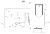
図4に遮蔽板105を折り曲げた遮蔽板109に変更したクリーニング装置100の構成を示す。
遮蔽板の折り曲げ角をθ’とすれば、一次電子の照射角度θとθ’は等しい角度となる。そのため、図4に示す通り、折り曲げた遮蔽板109を利用することで一次電子の入射角度が大きくなるため、二次電子の発生効率が上昇しクリーニングの効率化が図れると考えられる。
104 バイアス電源、105 遮蔽板、106 電流計、107 制御器、108 記憶部、109 遮蔽板、110 バイアス電源、111 荷電粒子線装置、112 鏡筒、113 荷電粒子源、114 真空ポンプ
Claims (6)
- 荷電粒子源を有する鏡筒に接続された試料室と、
前記試料室に配置される電子源と、
前記電子源の前面に設置された遮蔽板と、を備え、
前記電子源から放出される一次電子が前記遮蔽板に衝突することで放出される二次電子であって、炭化水素系ガスの脱離現象を起こす1eV以下のエネルギーの二次電子により、前記試料室内のクリーニングを行う、ことを特徴とするクリーニング装置。 - 請求項1記載のクリーニング装置であって、
前記遮蔽板は、前記電子源から放出された前記一次電子が、直接前記試料室の内部に照射されないように配置される、ことを特徴としたクリーニング装置。 - 請求項1記載のクリーニング装置であって、
前記遮蔽板は、取り外し交換が可能である、ことを特徴とするクリーニング装置。 - 請求項1記載のクリーニング装置であって、
前記遮蔽板は、二次電子放出効率が大きい材料で構成されている、又は、表面に二次電子放出効率が大きい材料が塗布されている、ことを特徴とするクリーニング装置。 - 請求項1記載のクリーニング装置であって、
前記電子源はフィラメントからなり、
前記遮蔽板は、前記フィラメントに対する設置角度を変更し、前記二次電子の放出率を高くする、ことを特徴とするクリーニング装置。 - 請求項1記載のクリーニング装置であって、
前記遮蔽板に接続されるバイアス電源を更に備え、
前記バイアス電源により前記遮蔽板に負電圧を印加し、前記二次電子の放出量を増加させる、ことを特徴とするクリーニング装置。
Applications Claiming Priority (1)
| Application Number | Priority Date | Filing Date | Title |
|---|---|---|---|
| PCT/JP2021/048174 WO2023119619A1 (ja) | 2021-12-24 | 2021-12-24 | 電子クリーニング装置 |
Publications (3)
| Publication Number | Publication Date |
|---|---|
| JPWO2023119619A1 JPWO2023119619A1 (ja) | 2023-06-29 |
| JPWO2023119619A5 JPWO2023119619A5 (ja) | 2024-10-07 |
| JP7610040B2 true JP7610040B2 (ja) | 2025-01-07 |
Family
ID=86901824
Family Applications (1)
| Application Number | Title | Priority Date | Filing Date |
|---|---|---|---|
| JP2023568986A Active JP7610040B2 (ja) | 2021-12-24 | 2021-12-24 | 電子クリーニング装置 |
Country Status (4)
| Country | Link |
|---|---|
| US (1) | US20250037962A1 (ja) |
| JP (1) | JP7610040B2 (ja) |
| KR (1) | KR102826181B1 (ja) |
| WO (1) | WO2023119619A1 (ja) |
Citations (1)
| Publication number | Priority date | Publication date | Assignee | Title |
|---|---|---|---|---|
| WO2019155540A1 (ja) | 2018-02-07 | 2019-08-15 | 株式会社日立ハイテクノロジーズ | クリーニング装置 |
Family Cites Families (5)
| Publication number | Priority date | Publication date | Assignee | Title |
|---|---|---|---|---|
| JPH0684850A (ja) * | 1992-09-02 | 1994-03-25 | Hitachi Ltd | 減圧容器のクリーニング方法および装置 |
| JPH06267493A (ja) * | 1993-03-16 | 1994-09-22 | Hitachi Ltd | チャージアップ防止装置及び方法 |
| JP2010103072A (ja) | 2008-10-21 | 2010-05-06 | Hironari Miyazaki | 電子顕微鏡試料室用ベーキング機構 |
| JP6229404B2 (ja) | 2013-09-27 | 2017-11-15 | ウシオ電機株式会社 | エキシマランプ装置および光照射処理装置 |
| KR101530282B1 (ko) | 2014-09-03 | 2015-06-24 | 히타치하이테크놀로지즈코리아 주식회사 | 전자현미경 플라즈마 클리너 |
-
2021
- 2021-12-24 US US18/716,198 patent/US20250037962A1/en active Pending
- 2021-12-24 JP JP2023568986A patent/JP7610040B2/ja active Active
- 2021-12-24 KR KR1020247016581A patent/KR102826181B1/ko active Active
- 2021-12-24 WO PCT/JP2021/048174 patent/WO2023119619A1/ja not_active Ceased
Patent Citations (1)
| Publication number | Priority date | Publication date | Assignee | Title |
|---|---|---|---|---|
| WO2019155540A1 (ja) | 2018-02-07 | 2019-08-15 | 株式会社日立ハイテクノロジーズ | クリーニング装置 |
Also Published As
| Publication number | Publication date |
|---|---|
| JPWO2023119619A1 (ja) | 2023-06-29 |
| KR20240090546A (ko) | 2024-06-21 |
| WO2023119619A1 (ja) | 2023-06-29 |
| US20250037962A1 (en) | 2025-01-30 |
| KR102826181B1 (ko) | 2025-06-27 |
Similar Documents
| Publication | Publication Date | Title |
|---|---|---|
| US8279397B2 (en) | Method for removing contamination on optical surfaces and optical arrangement | |
| US10840054B2 (en) | Charged-particle source and method for cleaning a charged-particle source using back-sputtering | |
| US20130255717A1 (en) | System and method for cleaning surfaces and components of mask and wafer inspection systems based on the positive column of a glow discharge plasma | |
| Nishimori et al. | Experimental investigation of an optimum configuration for a high-voltage photoemission gun for operation at≥ 500 kV | |
| TWI748477B (zh) | 電子束裝置及電子束裝置之控制方法 | |
| US20140252953A1 (en) | Plasma generator | |
| EP3518268B1 (en) | Charged-particle source and method for cleaning a charged-particle source using back-sputtering | |
| US7871677B2 (en) | Surface treating method for substrate | |
| JP7610040B2 (ja) | 電子クリーニング装置 | |
| JPS62206753A (ja) | プラズマx線発生装置 | |
| JP7132254B2 (ja) | クリーニング装置 | |
| Chalise et al. | Side-extraction-type secondary emission electron gun using wire ion plasma source | |
| CN114566420A (zh) | 质量分析装置 | |
| Wang | Particles scattering in a HVDC gun | |
| JPH0629251A (ja) | 中性粒子ビームエッチング装置 | |
| KR102243549B1 (ko) | 중이온 빔 발생 장치 및 방법 | |
| KR20180019475A (ko) | 플라즈마 세정기에 사용되는 자석 | |
| JPH0676782A (ja) | イオンビーム加工装置 | |
| JP3100006B2 (ja) | 放射光発生装置 | |
| JP2001126657A (ja) | 電子真空ポンプ | |
| JP2025160149A (ja) | 基材をコーティングする方法 | |
| JPH0822787A (ja) | 電界放射型電子銃 | |
| JP2006104522A (ja) | 薄膜形成方法および薄膜形成装置 | |
| JPH03219541A (ja) | プラズマ処理装置 | |
| WO2015115000A1 (ja) | オービトロンポンプを備えた電子線装置、およびその電子線照射方法 |
Legal Events
| Date | Code | Title | Description |
|---|---|---|---|
| A529 | Written submission of copy of amendment under article 34 pct |
Free format text: JAPANESE INTERMEDIATE CODE: A5211 Effective date: 20240611 |
|
| A621 | Written request for application examination |
Free format text: JAPANESE INTERMEDIATE CODE: A621 Effective date: 20240611 |
|
| TRDD | Decision of grant or rejection written | ||
| A01 | Written decision to grant a patent or to grant a registration (utility model) |
Free format text: JAPANESE INTERMEDIATE CODE: A01 Effective date: 20241210 |
|
| A61 | First payment of annual fees (during grant procedure) |
Free format text: JAPANESE INTERMEDIATE CODE: A61 Effective date: 20241219 |
|
| R150 | Certificate of patent or registration of utility model |
Ref document number: 7610040 Country of ref document: JP Free format text: JAPANESE INTERMEDIATE CODE: R150 |