JPWO2015019643A1 - サーミスタ素子 - Google Patents
サーミスタ素子 Download PDFInfo
- Publication number
- JPWO2015019643A1 JPWO2015019643A1 JP2015530718A JP2015530718A JPWO2015019643A1 JP WO2015019643 A1 JPWO2015019643 A1 JP WO2015019643A1 JP 2015530718 A JP2015530718 A JP 2015530718A JP 2015530718 A JP2015530718 A JP 2015530718A JP WO2015019643 A1 JPWO2015019643 A1 JP WO2015019643A1
- Authority
- JP
- Japan
- Prior art keywords
- thermistor
- electrode
- main body
- thermistor element
- main
- Prior art date
- Legal status (The legal status is an assumption and is not a legal conclusion. Google has not performed a legal analysis and makes no representation as to the accuracy of the status listed.)
- Pending
Links
Images


Classifications
-
- H—ELECTRICITY
- H01—ELECTRIC ELEMENTS
- H01C—RESISTORS
- H01C7/00—Non-adjustable resistors formed as one or more layers or coatings; Non-adjustable resistors made from powdered conducting material or powdered semi-conducting material with or without insulating material
- H01C7/008—Thermistors
-
- H—ELECTRICITY
- H01—ELECTRIC ELEMENTS
- H01C—RESISTORS
- H01C1/00—Details
- H01C1/14—Terminals or tapping points specially adapted for resistors; Arrangements of terminals or tapping points on resistors
- H01C1/1413—Terminals or electrodes formed on resistive elements having negative temperature coefficient
-
- H—ELECTRICITY
- H01—ELECTRIC ELEMENTS
- H01C—RESISTORS
- H01C1/00—Details
- H01C1/14—Terminals or tapping points specially adapted for resistors; Arrangements of terminals or tapping points on resistors
- H01C1/148—Terminals or tapping points specially adapted for resistors; Arrangements of terminals or tapping points on resistors the terminals embracing or surrounding the resistive element
-
- H—ELECTRICITY
- H01—ELECTRIC ELEMENTS
- H01C—RESISTORS
- H01C7/00—Non-adjustable resistors formed as one or more layers or coatings; Non-adjustable resistors made from powdered conducting material or powdered semi-conducting material with or without insulating material
- H01C7/04—Non-adjustable resistors formed as one or more layers or coatings; Non-adjustable resistors made from powdered conducting material or powdered semi-conducting material with or without insulating material having negative temperature coefficient
- H01C7/041—Non-adjustable resistors formed as one or more layers or coatings; Non-adjustable resistors made from powdered conducting material or powdered semi-conducting material with or without insulating material having negative temperature coefficient formed with two or more layers
Landscapes
- Engineering & Computer Science (AREA)
- Microelectronics & Electronic Packaging (AREA)
- Physics & Mathematics (AREA)
- Electromagnetism (AREA)
- Thermistors And Varistors (AREA)
Applications Claiming Priority (3)
| Application Number | Priority Date | Filing Date | Title |
|---|---|---|---|
| JP2013164902 | 2013-08-08 | ||
| JP2013164902 | 2013-08-08 | ||
| PCT/JP2014/055259 WO2015019643A1 (fr) | 2013-08-08 | 2014-03-03 | Élément de thermistance |
Publications (1)
| Publication Number | Publication Date |
|---|---|
| JPWO2015019643A1 true JPWO2015019643A1 (ja) | 2017-03-02 |
Family
ID=52460992
Family Applications (1)
| Application Number | Title | Priority Date | Filing Date |
|---|---|---|---|
| JP2015530718A Pending JPWO2015019643A1 (ja) | 2013-08-08 | 2014-03-03 | サーミスタ素子 |
Country Status (3)
| Country | Link |
|---|---|
| US (1) | US20160155546A1 (fr) |
| JP (1) | JPWO2015019643A1 (fr) |
| WO (1) | WO2015019643A1 (fr) |
Families Citing this family (2)
| Publication number | Priority date | Publication date | Assignee | Title |
|---|---|---|---|---|
| DE102015121982A1 (de) * | 2015-12-16 | 2017-06-22 | Epcos Ag | NTC-Keramik, elektronisches Bauelement zur Einschaltstrombegrenzung und Verfahren zur Herstellung eines elektronischen Bauelements |
| DE112019002039T5 (de) | 2018-04-17 | 2021-03-11 | Avx Corporation | Varistor mit Hochtemperaturanwendungen |
Citations (4)
| Publication number | Priority date | Publication date | Assignee | Title |
|---|---|---|---|---|
| JPH09180907A (ja) * | 1995-10-27 | 1997-07-11 | Murata Mfg Co Ltd | 積層複合セラミックとそれを用いた積層複合セラミック素子 |
| JP2001143904A (ja) * | 1999-11-18 | 2001-05-25 | Matsushita Electric Ind Co Ltd | 複合積層サーミスタ |
| JP2003272904A (ja) * | 2002-03-19 | 2003-09-26 | Tdk Corp | 複合型積層チップntcサーミスタ |
| JP2005294476A (ja) * | 2004-03-31 | 2005-10-20 | Mitsubishi Materials Corp | 表面実装型温度検出素子 |
Family Cites Families (1)
| Publication number | Priority date | Publication date | Assignee | Title |
|---|---|---|---|---|
| JP2540440Y2 (ja) * | 1990-04-24 | 1997-07-02 | 株式会社芝浦電子 | チップ形サーミスタセンサ |
-
2014
- 2014-03-03 JP JP2015530718A patent/JPWO2015019643A1/ja active Pending
- 2014-03-03 WO PCT/JP2014/055259 patent/WO2015019643A1/fr not_active Ceased
-
2016
- 2016-02-05 US US15/016,852 patent/US20160155546A1/en not_active Abandoned
Patent Citations (4)
| Publication number | Priority date | Publication date | Assignee | Title |
|---|---|---|---|---|
| JPH09180907A (ja) * | 1995-10-27 | 1997-07-11 | Murata Mfg Co Ltd | 積層複合セラミックとそれを用いた積層複合セラミック素子 |
| JP2001143904A (ja) * | 1999-11-18 | 2001-05-25 | Matsushita Electric Ind Co Ltd | 複合積層サーミスタ |
| JP2003272904A (ja) * | 2002-03-19 | 2003-09-26 | Tdk Corp | 複合型積層チップntcサーミスタ |
| JP2005294476A (ja) * | 2004-03-31 | 2005-10-20 | Mitsubishi Materials Corp | 表面実装型温度検出素子 |
Also Published As
| Publication number | Publication date |
|---|---|
| WO2015019643A1 (fr) | 2015-02-12 |
| US20160155546A1 (en) | 2016-06-02 |
Similar Documents
| Publication | Publication Date | Title |
|---|---|---|
| CN109427459B (zh) | 线圈部件 | |
| CN104813419B (zh) | 热敏电阻装置 | |
| KR101663510B1 (ko) | 정전기 보호 부품 | |
| JP2014222812A (ja) | 発振デバイス | |
| JP5324390B2 (ja) | 積層電子部品 | |
| CN111133548A (zh) | 片式熔断器 | |
| CN206179618U (zh) | 温度传感器 | |
| JP2015129731A (ja) | 温度センサ | |
| WO2012114857A1 (fr) | Structure de montage de composant électronique | |
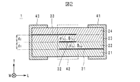
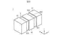
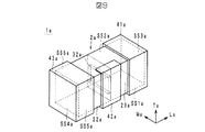
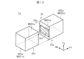
| JPWO2015019643A1 (ja) | サーミスタ素子 | |
| CN109328296B (zh) | 温度传感器以及温度测定装置 | |
| KR102117482B1 (ko) | 서미스터용 조성물 및 그를 이용한 서미스터 | |
| WO2021065807A1 (fr) | Élément de thermistance ntc | |
| JP5846305B2 (ja) | Ntcサーミスタ素子およびその製造方法 | |
| CN104008830B (zh) | 芯片型正特性热敏电阻元件 | |
| CN203311954U (zh) | 层叠型ptc热敏电阻 | |
| JP6828256B2 (ja) | Ntcサーミスタ素子 | |
| JP6252020B2 (ja) | 静電気保護部品及び静電気保護部品の製造方法 | |
| TW201530107A (zh) | 溫度感測器及製造方法 | |
| JP5908792B2 (ja) | コイル内蔵配線基板および電子装置 | |
| JP7434863B2 (ja) | Ntcサーミスタ素子 | |
| JP2018026521A (ja) | 厚膜型サーミスタ | |
| WO2013168311A1 (fr) | Elément varistance de puce et méthode de fabrication de celui-ci | |
| WO2015019644A1 (fr) | Composant électronique et procédé de fabrication de ce composant électronique | |
| TWI497536B (zh) | Chip type positive characteristic thermal resistance element |
Legal Events
| Date | Code | Title | Description |
|---|---|---|---|
| A131 | Notification of reasons for refusal |
Free format text: JAPANESE INTERMEDIATE CODE: A131 Effective date: 20170124 |
|
| A521 | Request for written amendment filed |
Free format text: JAPANESE INTERMEDIATE CODE: A523 Effective date: 20170324 |
|
| A131 | Notification of reasons for refusal |
Free format text: JAPANESE INTERMEDIATE CODE: A131 Effective date: 20170516 |
|
| A02 | Decision of refusal |
Free format text: JAPANESE INTERMEDIATE CODE: A02 Effective date: 20171114 |