KR20110051160A - 딥 트렌치 라이너 제거 처리 - Google Patents
딥 트렌치 라이너 제거 처리 Download PDFInfo
- Publication number
- KR20110051160A KR20110051160A KR1020100111090A KR20100111090A KR20110051160A KR 20110051160 A KR20110051160 A KR 20110051160A KR 1020100111090 A KR1020100111090 A KR 1020100111090A KR 20100111090 A KR20100111090 A KR 20100111090A KR 20110051160 A KR20110051160 A KR 20110051160A
- Authority
- KR
- South Korea
- Prior art keywords
- liner
- conformal
- protective layer
- substrate
- gas
- Prior art date
- Legal status (The legal status is an assumption and is not a legal conclusion. Google has not performed a legal analysis and makes no representation as to the accuracy of the status listed.)
- Granted
Links
Images


Classifications
-
- H—ELECTRICITY
- H10—SEMICONDUCTOR DEVICES; ELECTRIC SOLID-STATE DEVICES NOT OTHERWISE PROVIDED FOR
- H10P—GENERIC PROCESSES OR APPARATUS FOR THE MANUFACTURE OR TREATMENT OF DEVICES COVERED BY CLASS H10
- H10P50/00—Etching of wafers, substrates or parts of devices
- H10P50/73—Etching of wafers, substrates or parts of devices using masks for insulating materials
-
- H—ELECTRICITY
- H01—ELECTRIC ELEMENTS
- H01J—ELECTRIC DISCHARGE TUBES OR DISCHARGE LAMPS
- H01J37/00—Discharge tubes with provision for introducing objects or material to be exposed to the discharge, e.g. for the purpose of examination or processing thereof
- H01J37/32—Gas-filled discharge tubes
- H01J37/32009—Arrangements for generation of plasma specially adapted for examination or treatment of objects, e.g. plasma sources
- H01J37/32082—Radio frequency generated discharge
- H01J37/32091—Radio frequency generated discharge the radio frequency energy being capacitively coupled to the plasma
-
- H—ELECTRICITY
- H01—ELECTRIC ELEMENTS
- H01J—ELECTRIC DISCHARGE TUBES OR DISCHARGE LAMPS
- H01J37/00—Discharge tubes with provision for introducing objects or material to be exposed to the discharge, e.g. for the purpose of examination or processing thereof
- H01J37/32—Gas-filled discharge tubes
- H01J37/32009—Arrangements for generation of plasma specially adapted for examination or treatment of objects, e.g. plasma sources
- H01J37/32082—Radio frequency generated discharge
- H01J37/321—Radio frequency generated discharge the radio frequency energy being inductively coupled to the plasma
-
- H—ELECTRICITY
- H01—ELECTRIC ELEMENTS
- H01J—ELECTRIC DISCHARGE TUBES OR DISCHARGE LAMPS
- H01J37/00—Discharge tubes with provision for introducing objects or material to be exposed to the discharge, e.g. for the purpose of examination or processing thereof
- H01J37/32—Gas-filled discharge tubes
- H01J37/32009—Arrangements for generation of plasma specially adapted for examination or treatment of objects, e.g. plasma sources
- H01J37/32082—Radio frequency generated discharge
- H01J37/32137—Radio frequency generated discharge controlling of the discharge by modulation of energy
- H01J37/32155—Frequency modulation
- H01J37/32165—Plural frequencies
-
- H—ELECTRICITY
- H01—ELECTRIC ELEMENTS
- H01J—ELECTRIC DISCHARGE TUBES OR DISCHARGE LAMPS
- H01J37/00—Discharge tubes with provision for introducing objects or material to be exposed to the discharge, e.g. for the purpose of examination or processing thereof
- H01J37/32—Gas-filled discharge tubes
- H01J37/32009—Arrangements for generation of plasma specially adapted for examination or treatment of objects, e.g. plasma sources
- H01J37/32192—Microwave generated discharge
-
- H—ELECTRICITY
- H01—ELECTRIC ELEMENTS
- H01J—ELECTRIC DISCHARGE TUBES OR DISCHARGE LAMPS
- H01J37/00—Discharge tubes with provision for introducing objects or material to be exposed to the discharge, e.g. for the purpose of examination or processing thereof
- H01J37/32—Gas-filled discharge tubes
- H01J37/32431—Constructional details of the reactor
- H01J37/3244—Gas supply means
- H01J37/32449—Gas control, e.g. control of the gas flow
-
- H—ELECTRICITY
- H01—ELECTRIC ELEMENTS
- H01J—ELECTRIC DISCHARGE TUBES OR DISCHARGE LAMPS
- H01J37/00—Discharge tubes with provision for introducing objects or material to be exposed to the discharge, e.g. for the purpose of examination or processing thereof
- H01J37/32—Gas-filled discharge tubes
- H01J37/32431—Constructional details of the reactor
- H01J37/3266—Magnetic control means
-
- H—ELECTRICITY
- H10—SEMICONDUCTOR DEVICES; ELECTRIC SOLID-STATE DEVICES NOT OTHERWISE PROVIDED FOR
- H10D—INORGANIC ELECTRIC SEMICONDUCTOR DEVICES
- H10D1/00—Resistors, capacitors or inductors
- H10D1/01—Manufacture or treatment
- H10D1/045—Manufacture or treatment of capacitors having potential barriers, e.g. varactors
- H10D1/047—Manufacture or treatment of capacitors having potential barriers, e.g. varactors of conductor-insulator-semiconductor capacitors, e.g. trench capacitors
-
- H—ELECTRICITY
- H10—SEMICONDUCTOR DEVICES; ELECTRIC SOLID-STATE DEVICES NOT OTHERWISE PROVIDED FOR
- H10P—GENERIC PROCESSES OR APPARATUS FOR THE MANUFACTURE OR TREATMENT OF DEVICES COVERED BY CLASS H10
- H10P50/00—Etching of wafers, substrates or parts of devices
- H10P50/20—Dry etching; Plasma etching; Reactive-ion etching
- H10P50/28—Dry etching; Plasma etching; Reactive-ion etching of insulating materials
- H10P50/282—Dry etching; Plasma etching; Reactive-ion etching of insulating materials of inorganic materials
- H10P50/283—Dry etching; Plasma etching; Reactive-ion etching of insulating materials of inorganic materials by chemical means
- H10P50/285—Dry etching; Plasma etching; Reactive-ion etching of insulating materials of inorganic materials by chemical means of materials not containing Si, e.g. PZT or Al2O3
-
- H—ELECTRICITY
- H10—SEMICONDUCTOR DEVICES; ELECTRIC SOLID-STATE DEVICES NOT OTHERWISE PROVIDED FOR
- H10P—GENERIC PROCESSES OR APPARATUS FOR THE MANUFACTURE OR TREATMENT OF DEVICES COVERED BY CLASS H10
- H10P72/00—Handling or holding of wafers, substrates or devices during manufacture or treatment thereof
- H10P72/04—Apparatus for manufacture or treatment
- H10P72/0402—Apparatus for fluid treatment
- H10P72/0418—Apparatus for fluid treatment for etching
- H10P72/0421—Apparatus for fluid treatment for etching for drying etching
-
- H—ELECTRICITY
- H10—SEMICONDUCTOR DEVICES; ELECTRIC SOLID-STATE DEVICES NOT OTHERWISE PROVIDED FOR
- H10P—GENERIC PROCESSES OR APPARATUS FOR THE MANUFACTURE OR TREATMENT OF DEVICES COVERED BY CLASS H10
- H10P72/00—Handling or holding of wafers, substrates or devices during manufacture or treatment thereof
- H10P72/04—Apparatus for manufacture or treatment
- H10P72/0451—Apparatus for manufacturing or treating in a plurality of work-stations
- H10P72/0462—Apparatus for manufacturing or treating in a plurality of work-stations characterised by the construction of the processing chambers, e.g. modular processing chambers
-
- H—ELECTRICITY
- H10—SEMICONDUCTOR DEVICES; ELECTRIC SOLID-STATE DEVICES NOT OTHERWISE PROVIDED FOR
- H10P—GENERIC PROCESSES OR APPARATUS FOR THE MANUFACTURE OR TREATMENT OF DEVICES COVERED BY CLASS H10
- H10P72/00—Handling or holding of wafers, substrates or devices during manufacture or treatment thereof
- H10P72/06—Apparatus for monitoring, sorting, marking, testing or measuring
- H10P72/0604—Process monitoring, e.g. flow or thickness monitoring
-
- H—ELECTRICITY
- H10—SEMICONDUCTOR DEVICES; ELECTRIC SOLID-STATE DEVICES NOT OTHERWISE PROVIDED FOR
- H10P—GENERIC PROCESSES OR APPARATUS FOR THE MANUFACTURE OR TREATMENT OF DEVICES COVERED BY CLASS H10
- H10P72/00—Handling or holding of wafers, substrates or devices during manufacture or treatment thereof
- H10P72/70—Handling or holding of wafers, substrates or devices during manufacture or treatment thereof for supporting or gripping
- H10P72/72—Handling or holding of wafers, substrates or devices during manufacture or treatment thereof for supporting or gripping using electrostatic chucks
Landscapes
- Physics & Mathematics (AREA)
- Engineering & Computer Science (AREA)
- Plasma & Fusion (AREA)
- Chemical & Material Sciences (AREA)
- Analytical Chemistry (AREA)
- Drying Of Semiconductors (AREA)
- Plasma Technology (AREA)
Abstract
Description
도 2는 다른 실시예에 따른 라이너 제거 처리를 수행하는 흐름도를 제공한다.
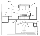
도 3은 실시예에 따른 처리 시스템의 개략도를 도시한다.
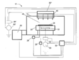
도 4는 다른 실시예에 따른 처리 시스템의 개략도를 도시한다.
도 5는 다른 실시예에 따른 처리 시스템의 개략도를 도시한다.
도 6은 다른 실시예에 따른 처리 시스템의 개략도를 도시한다.
도 7은 다른 실시예에 따른 처리 시스템의 개략도를 도시한다.
도 8은 다른 실시예에 따른 처리 시스템의 개략도를 도시한다.
도 9는 다른 실시예에 따른 처리 시스템의 개략도를 도시한다.
| 산화/에칭 조건 |
압력 (mtorr) |
UEL 전력 (W) |
LEL 전력 (W) |
O2 유속 (sccm) |
BCl3 유속 (sccm) |
C2H4 유속 (sccm) |
He 유속 (sccm) |
시간 (sec) |
| 참조 | 20 | 600 | 0 | 0 | 150 | 0 | 150 | 180 |
| 1 (산화) 2 (에칭) |
10 | 400 | 0 | 200 | 0 | 0 | 0 | 60 |
| 10 | 600 | 0 | 0 | 150 | 1 | 150 | 173.4 |
Claims (20)
- 라이너(liner) 제거 처리로서,
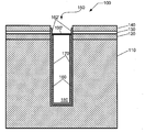
기판에 트렌치(trench)를 형성하는 단계;
상기 트렌치 내에 컨포멀(conformal) 라이너를 증착시키는 단계;
상기 트렌치를 벌크 충전 재료로 충전하는 단계; 및
상기 벌크 충전 재료의 노출면 상에 보호층을 형성하는 것과, 상기 컨포멀 라이너를 에칭하는 것을 교대로 행함으로써 상기 컨포멀 라이너의 잉여 부분을 선택적으로 제거하는 단계
를 포함하는 라이너 제거 처리. - 제 1 항에 있어서, 상기 벌크 충전 재료는 다결정 실리콘을 포함하는 것인 라이너 제거 처리 방법.
- 제 1 항에 있어서, 상기 컨포멀 라이너는 고 유전 상수(하이-k)층을 포함하는 것인 라이너 제거 처리 방법.
- 제 1 항에 있어서, 상기 컨포멀 라이너는 하프늄을 포함하는 것인 라이너 제거 처리 방법.
- 제 1 항에 있어서, 상기 보호층을 형성하는 것은, 상기 벌크 충전 재료의 상기 노출면 상에 상기 보호층을 증착시키는 단계, 또는 상기 벌크 충전 재료의 상기 노출면 상에 상기 보호층을 성장시키는 단계, 또는 상기 벌크 충전 재료의 상기 노출면 상에 상기 보호층을 증착시키는 단계와 성장시키는 단계 모두를 포함하는 것인 라이너 제거 처리 방법.
- 제 1 항에 있어서, 상기 보호층을 형성하는 것은, 상기 벌크 충전 재료의 상기 노출면을 산화시키는 단계를 포함하는 것인 라이너 제거 처리 방법.
- 제 1 항에 있어서, 상기 보호층을 형성하는 것은, O 라디칼, O2, 오존, CO, CO2, NO, N2O, 또는 NO2로 구성된 그룹으로부터 선택된 산소 함유 가스에 상기 기판을 노출시키는 단계를 포함하는 것인 라이너 제거 처리 방법.
- 제 1 항에 있어서, 상기 보호층을 형성하는 것은, 상기 기판을 비플라즈마 가스 환경에 노출시키는 단계를 포함하는 것인 라이너 제거 처리 방법.
- 제 1 항에 있어서, 상기 보호층을 형성하는 것은, 상기 기판을 플라즈마에 노출시키는 단계를 포함하는 것인 라이너 제거 처리 방법.
- 제 1 항에 있어서, 상기 보호층을 형성하는 것은, 상기 기판을 이온 빔 또는 가스 클러스터 이온 빔에 노출시키는 단계를 포함하는 것인 라이너 제거 처리 방법.
- 제 1 항에 있어서, 상기 보호층을 형성하는 것은, 상기 보호층을 기상 증착 처리를 사용하여 상기 기판 상에 증착시키는 단계를 포함하는 것인 라이너 제거 처리 방법.
- 제 1 항에 있어서, 상기 컨포멀 라이너를 에칭하는 것은, 습식 에칭 처리, 또는 건식 에칭 처리, 또는 양쪽 모두를 수행하는 단계를 포함하는 것인 라이너 제거 처리 방법.
- 제 1 항에 있어서, 상기 컨포멀 라이너를 에칭하는 것은, 할로겐 함유 가스와 선택적인 희가스(noble gas)를 갖는 처리 가스를 사용하여 플라즈마 에칭 처리를 수행하는 단계를 포함하는 것인 라이너 제거 처리 방법.
- 제 13 항에 있어서, 상기 할로겐 함유 가스는 HBr, Cl2, 또는 BCl3로 구성된 그룹으로부터 선택되는 것인 라이너 제거 처리 방법.
- 제 13 항에 있어서, 상기 처리 가스는 탄화수소 가스를 더 포함하는 것인 라이너 제거 처리 방법.
- 제 15 항에 있어서, 상기 탄화수소 가스는, C2H4, CH4, C2H2, C2H6, C3H4, C3H6, C3H8, C4H6, C4H8, C4H10, C5H8, C5H10, C6H6, C6H10 및 C6H12로 구성된 그룹으로부터 선택되는 것인 라이너 제거 처리 방법.
- 제 1 항에 있어서, 상기 보호층을 형성하는 것은 상기 컨포멀 라이너를 에칭하는 것에 선행하고, 상기 에칭은 상기 보호층을 실질적으로 소모하는 데 충분한 기간동안 수행되는 것인 라이너 제거 처리 방법.
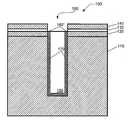
- 라이너 제거 처리로서,
기판에 트렌치를 형성하는 단계;
상기 트렌치 내에 컨포멀 하이-k 라이너를 증착시키는 단계;
상기 트렌치를 폴리실리콘층으로 충전하는 단계; 및
상기 트렌치 내의 상기 폴리실리콘층의 노출면층을 산소 함유 플라즈마에 노출시킴으로써 상기 폴리실리콘층의 노출면을 산화시키는 단계,
상기 산화시키는 단계에 이어, 할로겐 함유 가스를 갖는 처리 가스로 형성된 플라즈마를 사용하여 상기 컨포멀 하이-k 라이너를 에칭하는 단계, 및
상기 컨포멀 하이-k 라이너의 잉여 부분이 실질적으로 제거될 때까지 상기 산화시키는 단계와 상기 에칭하는 단계를 반복하는 단계
를 수행함으로써 상기 컨포멀 하이-k 라이너의 잉여 부분을 선택적으로 제거하는 단계
를 포함하는 라이너 제거 처리. - 제 18 항에 있어서, 상기 컨포멀 하이-k층은 하프늄을 포함하고, 상기 처리 가스는 BCl3 및 탄화수소 가스를 포함하는 것인 라이너 제거 처리 방법.
- 제 18 항에 있어서, 상기 컨포멀 하이-k 라이너의 상기 잉여 부분을 선택적으로 제거하는 단계를 위한 에칭 선택도는 약 30:1보다 크며, 상기 에칭 선택도는 상기 폴리실리콘층의 에칭률에 대한 상기 컨포멀 하이-k 라이너의 에칭률의 비를 나타내는 것인 라이너 제거 처리 방법.
Applications Claiming Priority (2)
| Application Number | Priority Date | Filing Date | Title |
|---|---|---|---|
| US12/614,496 | 2009-11-09 | ||
| US12/614,496 US8313661B2 (en) | 2009-11-09 | 2009-11-09 | Deep trench liner removal process |
Publications (2)
| Publication Number | Publication Date |
|---|---|
| KR20110051160A true KR20110051160A (ko) | 2011-05-17 |
| KR101713336B1 KR101713336B1 (ko) | 2017-03-07 |
Family
ID=43973372
Family Applications (1)
| Application Number | Title | Priority Date | Filing Date |
|---|---|---|---|
| KR1020100111090A Expired - Fee Related KR101713336B1 (ko) | 2009-11-09 | 2010-11-09 | 라이너의 제거 처리 방법 |
Country Status (5)
| Country | Link |
|---|---|
| US (1) | US8313661B2 (ko) |
| JP (1) | JP5633928B2 (ko) |
| KR (1) | KR101713336B1 (ko) |
| CN (1) | CN102087974B (ko) |
| TW (1) | TWI433263B (ko) |
Cited By (1)
| Publication number | Priority date | Publication date | Assignee | Title |
|---|---|---|---|---|
| KR20130025145A (ko) * | 2011-09-01 | 2013-03-11 | 세메스 주식회사 | 안테나 유닛 및 이를 포함하는 기판 처리 장치 |
Families Citing this family (6)
| Publication number | Priority date | Publication date | Assignee | Title |
|---|---|---|---|---|
| US8241944B2 (en) | 2010-07-02 | 2012-08-14 | Micron Technology, Inc. | Resistive RAM devices and methods |
| US20130075831A1 (en) * | 2011-09-24 | 2013-03-28 | Taiwan Semiconductor Manufacturing Company, Ltd. | Metal gate stack having tialn blocking/wetting layer |
| CN107431028A (zh) * | 2015-04-29 | 2017-12-01 | 英特尔公司 | 微电子导电路径和制作所述微电子导电路径的方法 |
| US10290739B2 (en) | 2017-09-29 | 2019-05-14 | Taiwan Semiconductor Manufacturing Co., Ltd. | Device and method of dielectric layer |
| US10170300B1 (en) * | 2017-11-30 | 2019-01-01 | Tokyo Electron Limited | Protective film forming method |
| US20250259891A1 (en) * | 2024-02-14 | 2025-08-14 | Tokyo Electron Limited | Protection structure for liner removal |
Citations (3)
| Publication number | Priority date | Publication date | Assignee | Title |
|---|---|---|---|---|
| JP2001177071A (ja) * | 1999-12-16 | 2001-06-29 | Toshiba Corp | 半導体装置および半導体装置の製造方法 |
| KR20060028636A (ko) * | 2003-05-30 | 2006-03-30 | 동경 엘렉트론 주식회사 | 고-k 유전성 재료 에칭 방법 및 시스템 |
| JP2006303010A (ja) * | 2005-04-18 | 2006-11-02 | Toshiba Corp | 半導体装置およびその製造方法 |
Family Cites Families (15)
| Publication number | Priority date | Publication date | Assignee | Title |
|---|---|---|---|---|
| JPH03187221A (ja) * | 1989-12-15 | 1991-08-15 | Sharp Corp | ドライエッチング装置 |
| US6146970A (en) * | 1998-05-26 | 2000-11-14 | Motorola Inc. | Capped shallow trench isolation and method of formation |
| US6074954A (en) * | 1998-08-31 | 2000-06-13 | Applied Materials, Inc | Process for control of the shape of the etch front in the etching of polysilicon |
| US6239476B1 (en) * | 1998-10-21 | 2001-05-29 | Advanced Micro Devices, Inc. | Integrated circuit isolation structure employing a protective layer and method for making same |
| US6080637A (en) * | 1998-12-07 | 2000-06-27 | Taiwan Semiconductor Manufacturing Company | Shallow trench isolation technology to eliminate a kink effect |
| US6331459B1 (en) * | 1999-02-18 | 2001-12-18 | Infineon Technologies Ag | Use of dummy poly spacers and divot fill techniques for DT-aligned processing after STI formation for advanced deep trench capacitor DRAM |
| EP1077475A3 (en) * | 1999-08-11 | 2003-04-02 | Applied Materials, Inc. | Method of micromachining a multi-part cavity |
| US20030222296A1 (en) * | 2002-06-04 | 2003-12-04 | Applied Materials, Inc. | Method of forming a capacitor using a high K dielectric material |
| JP2005039015A (ja) * | 2003-07-18 | 2005-02-10 | Hitachi High-Technologies Corp | プラズマ処理方法および装置 |
| JP2005045126A (ja) * | 2003-07-24 | 2005-02-17 | Semiconductor Leading Edge Technologies Inc | 半導体装置の製造方法 |
| US7285433B2 (en) * | 2003-11-06 | 2007-10-23 | General Electric Company | Integrated devices with optical and electrical isolation and method for making |
| US7015113B2 (en) * | 2004-04-01 | 2006-03-21 | Micron Technology, Inc. | Methods of forming trench isolation regions |
| EP1780779A3 (en) * | 2005-10-28 | 2008-06-11 | Interuniversitair Microelektronica Centrum ( Imec) | A plasma for patterning advanced gate stacks |
| JP2009021584A (ja) * | 2007-06-27 | 2009-01-29 | Applied Materials Inc | 高k材料ゲート構造の高温エッチング方法 |
| JP5607881B2 (ja) * | 2008-12-26 | 2014-10-15 | 東京エレクトロン株式会社 | 基板処理方法 |
-
2009
- 2009-11-09 US US12/614,496 patent/US8313661B2/en not_active Expired - Fee Related
-
2010
- 2010-11-05 JP JP2010248370A patent/JP5633928B2/ja not_active Expired - Fee Related
- 2010-11-09 TW TW099138497A patent/TWI433263B/zh not_active IP Right Cessation
- 2010-11-09 CN CN2010105410470A patent/CN102087974B/zh not_active Expired - Fee Related
- 2010-11-09 KR KR1020100111090A patent/KR101713336B1/ko not_active Expired - Fee Related
Patent Citations (3)
| Publication number | Priority date | Publication date | Assignee | Title |
|---|---|---|---|---|
| JP2001177071A (ja) * | 1999-12-16 | 2001-06-29 | Toshiba Corp | 半導体装置および半導体装置の製造方法 |
| KR20060028636A (ko) * | 2003-05-30 | 2006-03-30 | 동경 엘렉트론 주식회사 | 고-k 유전성 재료 에칭 방법 및 시스템 |
| JP2006303010A (ja) * | 2005-04-18 | 2006-11-02 | Toshiba Corp | 半導体装置およびその製造方法 |
Cited By (1)
| Publication number | Priority date | Publication date | Assignee | Title |
|---|---|---|---|---|
| KR20130025145A (ko) * | 2011-09-01 | 2013-03-11 | 세메스 주식회사 | 안테나 유닛 및 이를 포함하는 기판 처리 장치 |
Also Published As
| Publication number | Publication date |
|---|---|
| JP2011101017A (ja) | 2011-05-19 |
| TW201126646A (en) | 2011-08-01 |
| TWI433263B (zh) | 2014-04-01 |
| US8313661B2 (en) | 2012-11-20 |
| CN102087974A (zh) | 2011-06-08 |
| US20110108517A1 (en) | 2011-05-12 |
| KR101713336B1 (ko) | 2017-03-07 |
| JP5633928B2 (ja) | 2014-12-03 |
| CN102087974B (zh) | 2013-09-25 |
Similar Documents
| Publication | Publication Date | Title |
|---|---|---|
| TWI888341B (zh) | 用以改善使用電漿及/或熱處理之二氧化鉿基鐵電材料中的效能之方法 | |
| US9111746B2 (en) | Method for reducing damage to low-k gate spacer during etching | |
| CN101511969B (zh) | 用于干法刻蚀含铪材料的方法和系统 | |
| US8664125B2 (en) | Highly selective spacer etch process with reduced sidewall spacer slimming | |
| TWI514467B (zh) | 形成間隔物側壁上之含SiOCl的層以預防間隔物蝕刻時之臨界尺寸損失 | |
| KR101713336B1 (ko) | 라이너의 제거 처리 방법 | |
| TWI838267B (zh) | 薄膜及沉積薄膜的方法 | |
| US10777456B1 (en) | Semiconductor back end of line (BEOL) interconnect using multiple materials in a fully self-aligned via (FSAV) process | |
| TWI488235B (zh) | 全金屬閘極結構之圖案成形方法 | |
| US20060068603A1 (en) | A method for forming a thin complete high-permittivity dielectric layer | |
| US8501628B2 (en) | Differential metal gate etching process | |
| TWI423324B (zh) | 相對於其他材料具有高選擇率之金屬氮化物的蝕刻方法 | |
| US11749532B2 (en) | Methods and apparatus for processing a substrate |
Legal Events
| Date | Code | Title | Description |
|---|---|---|---|
| PA0109 | Patent application |
St.27 status event code: A-0-1-A10-A12-nap-PA0109 |
|
| P11-X000 | Amendment of application requested |
St.27 status event code: A-2-2-P10-P11-nap-X000 |
|
| P13-X000 | Application amended |
St.27 status event code: A-2-2-P10-P13-nap-X000 |
|
| PG1501 | Laying open of application |
St.27 status event code: A-1-1-Q10-Q12-nap-PG1501 |
|
| R17-X000 | Change to representative recorded |
St.27 status event code: A-3-3-R10-R17-oth-X000 |
|
| R17-X000 | Change to representative recorded |
St.27 status event code: A-3-3-R10-R17-oth-X000 |
|
| A201 | Request for examination | ||
| PA0201 | Request for examination |
St.27 status event code: A-1-2-D10-D11-exm-PA0201 |
|
| P22-X000 | Classification modified |
St.27 status event code: A-2-2-P10-P22-nap-X000 |
|
| D13-X000 | Search requested |
St.27 status event code: A-1-2-D10-D13-srh-X000 |
|
| D14-X000 | Search report completed |
St.27 status event code: A-1-2-D10-D14-srh-X000 |
|
| E902 | Notification of reason for refusal | ||
| PE0902 | Notice of grounds for rejection |
St.27 status event code: A-1-2-D10-D21-exm-PE0902 |
|
| T11-X000 | Administrative time limit extension requested |
St.27 status event code: U-3-3-T10-T11-oth-X000 |
|
| E13-X000 | Pre-grant limitation requested |
St.27 status event code: A-2-3-E10-E13-lim-X000 |
|
| P11-X000 | Amendment of application requested |
St.27 status event code: A-2-2-P10-P11-nap-X000 |
|
| P13-X000 | Application amended |
St.27 status event code: A-2-2-P10-P13-nap-X000 |
|
| E701 | Decision to grant or registration of patent right | ||
| PE0701 | Decision of registration |
St.27 status event code: A-1-2-D10-D22-exm-PE0701 |
|
| GRNT | Written decision to grant | ||
| PR0701 | Registration of establishment |
St.27 status event code: A-2-4-F10-F11-exm-PR0701 |
|
| PR1002 | Payment of registration fee |
St.27 status event code: A-2-2-U10-U11-oth-PR1002 Fee payment year number: 1 |
|
| PG1601 | Publication of registration |
St.27 status event code: A-4-4-Q10-Q13-nap-PG1601 |
|
| FPAY | Annual fee payment |
Payment date: 20200218 Year of fee payment: 4 |
|
| PR1001 | Payment of annual fee |
St.27 status event code: A-4-4-U10-U11-oth-PR1001 Fee payment year number: 4 |
|
| FPAY | Annual fee payment |
Payment date: 20210218 Year of fee payment: 5 |
|
| PR1001 | Payment of annual fee |
St.27 status event code: A-4-4-U10-U11-oth-PR1001 Fee payment year number: 5 |
|
| FPAY | Annual fee payment |
Payment date: 20220204 Year of fee payment: 6 |
|
| PR1001 | Payment of annual fee |
St.27 status event code: A-4-4-U10-U11-oth-PR1001 Fee payment year number: 6 |
|
| PC1903 | Unpaid annual fee |
St.27 status event code: A-4-4-U10-U13-oth-PC1903 Not in force date: 20230301 Payment event data comment text: Termination Category : DEFAULT_OF_REGISTRATION_FEE |
|
| PC1903 | Unpaid annual fee |
St.27 status event code: N-4-6-H10-H13-oth-PC1903 Ip right cessation event data comment text: Termination Category : DEFAULT_OF_REGISTRATION_FEE Not in force date: 20230301 |
|
| P22-X000 | Classification modified |
St.27 status event code: A-4-4-P10-P22-nap-X000 |