KR20110136498A - 반도체 소자의 제조 방법 - Google Patents
반도체 소자의 제조 방법 Download PDFInfo
- Publication number
- KR20110136498A KR20110136498A KR1020100056549A KR20100056549A KR20110136498A KR 20110136498 A KR20110136498 A KR 20110136498A KR 1020100056549 A KR1020100056549 A KR 1020100056549A KR 20100056549 A KR20100056549 A KR 20100056549A KR 20110136498 A KR20110136498 A KR 20110136498A
- Authority
- KR
- South Korea
- Prior art keywords
- film
- metal wiring
- semiconductor device
- metal
- barrier film
- Prior art date
- Legal status (The legal status is an assumption and is not a legal conclusion. Google has not performed a legal analysis and makes no representation as to the accuracy of the status listed.)
- Withdrawn
Links
Images


Classifications
-
- H—ELECTRICITY
- H10—SEMICONDUCTOR DEVICES; ELECTRIC SOLID-STATE DEVICES NOT OTHERWISE PROVIDED FOR
- H10W—GENERIC PACKAGES, INTERCONNECTIONS, CONNECTORS OR OTHER CONSTRUCTIONAL DETAILS OF DEVICES COVERED BY CLASS H10
- H10W20/00—Interconnections in chips, wafers or substrates
- H10W20/01—Manufacture or treatment
- H10W20/031—Manufacture or treatment of conductive parts of the interconnections
- H10W20/032—Manufacture or treatment of conductive parts of the interconnections of conductive barrier, adhesion or liner layers
- H10W20/033—Manufacture or treatment of conductive parts of the interconnections of conductive barrier, adhesion or liner layers in openings in dielectrics
-
- H—ELECTRICITY
- H10—SEMICONDUCTOR DEVICES; ELECTRIC SOLID-STATE DEVICES NOT OTHERWISE PROVIDED FOR
- H10W—GENERIC PACKAGES, INTERCONNECTIONS, CONNECTORS OR OTHER CONSTRUCTIONAL DETAILS OF DEVICES COVERED BY CLASS H10
- H10W20/00—Interconnections in chips, wafers or substrates
- H10W20/01—Manufacture or treatment
- H10W20/031—Manufacture or treatment of conductive parts of the interconnections
- H10W20/056—Manufacture or treatment of conductive parts of the interconnections by filling conductive material into holes, grooves or trenches
-
- H—ELECTRICITY
- H10—SEMICONDUCTOR DEVICES; ELECTRIC SOLID-STATE DEVICES NOT OTHERWISE PROVIDED FOR
- H10W—GENERIC PACKAGES, INTERCONNECTIONS, CONNECTORS OR OTHER CONSTRUCTIONAL DETAILS OF DEVICES COVERED BY CLASS H10
- H10W20/00—Interconnections in chips, wafers or substrates
- H10W20/01—Manufacture or treatment
- H10W20/031—Manufacture or treatment of conductive parts of the interconnections
- H10W20/062—Manufacture or treatment of conductive parts of the interconnections by smoothing of conductive parts, e.g. by planarisation
Landscapes
- Internal Circuitry In Semiconductor Integrated Circuit Devices (AREA)
Abstract
Description
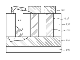
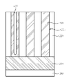
도 2a 내지 도 2d는 본 발명에 따른 반도체 소자의 제조 방법을 도시한 단면도들.
Claims (7)
- 반도체 기판에 제 1 금속 배선을 형성하는 단계;
상기 제 1 금속 배선을 포함한 전면에 절연막을 형성하는 단계;
콘택 플러그 마스크를 식각 마스크로 이용하여 상기 절연막을 식각하여 콘택홀을 형성하는 단계;
상기 콘택홀에 도전물질을 증착하여 콘택 플러그를 형성하는 단계;
상기 도전물질 상에 배리어막을 증착하는 단계; 및
상기 콘택 플러그와 접속되는 제 2 금속 배선을 형성하는 단계
를 포함하는 것을 특징으로 하는 반도체 소자의 제조 방법. - 제 1 항에 있어서,
상기 제 1 금속 배선은 배리어막 및 구리(Cu)막을 포함하는 것을 특징으로 하는 반도체 소자의 제조 방법. - 제 1 항에 있어서,
상기 도전물질은 텅스텐(W)을 포함하는 것을 특징으로 하는 반도체 소자의 제조 방법. - 제 1 항에 있어서,
상기 배리어막은 티타늄(Ti)과 티타늄질화막(TiN)이 적층된 구조로 형성하는 것을 특징으로 하는 반도체 소자의 제조 방법. - 제 4 항에 있어서,
상기 배리어막은 CVD(Chemical Vapor Deposition) 방법을 이용하여 형성하는 것을 특징으로 하는 반도체 소자의 제조 방법. - 제 1 항에 있어서,
상기 배리어막을 증착하는 단계 후, 상기 절연막이 노출될 때까지 상기 배리어막을 평탄화 식각하는 단계를 더 포함하는 것을 특징으로 하는 반도체 소자의 제조 방법. - 제 1 항에 있어서,
상기 제 2 금속 배선은 배리어막 및 구리(Cu)막을 포함하는 것을 특징으로 하는 반도체 소자의 제조 방법.
Priority Applications (1)
| Application Number | Priority Date | Filing Date | Title |
|---|---|---|---|
| KR1020100056549A KR20110136498A (ko) | 2010-06-15 | 2010-06-15 | 반도체 소자의 제조 방법 |
Applications Claiming Priority (1)
| Application Number | Priority Date | Filing Date | Title |
|---|---|---|---|
| KR1020100056549A KR20110136498A (ko) | 2010-06-15 | 2010-06-15 | 반도체 소자의 제조 방법 |
Publications (1)
| Publication Number | Publication Date |
|---|---|
| KR20110136498A true KR20110136498A (ko) | 2011-12-21 |
Family
ID=45503136
Family Applications (1)
| Application Number | Title | Priority Date | Filing Date |
|---|---|---|---|
| KR1020100056549A Withdrawn KR20110136498A (ko) | 2010-06-15 | 2010-06-15 | 반도체 소자의 제조 방법 |
Country Status (1)
| Country | Link |
|---|---|
| KR (1) | KR20110136498A (ko) |
-
2010
- 2010-06-15 KR KR1020100056549A patent/KR20110136498A/ko not_active Withdrawn
Similar Documents
| Publication | Publication Date | Title |
|---|---|---|
| KR100385227B1 (ko) | 구리 다층 배선을 가지는 반도체 장치 및 그 형성방법 | |
| CN100555598C (zh) | 埋入的金属双重镶嵌板电容器 | |
| US20100314765A1 (en) | Interconnection structure of semiconductor integrated circuit and method for making the same | |
| KR20250107287A (ko) | 완전히 정렬된 비아의 비아 사전충진 | |
| US20170110369A1 (en) | Electronic device and method for producing same | |
| KR20090045198A (ko) | 상호접속 구조물 및 상호접속 구조물의 제조 공정 | |
| KR20080061030A (ko) | 반도체 소자의 금속 배선 형성 방법 | |
| US7196423B2 (en) | Interconnect structure with dielectric barrier and fabrication method thereof | |
| US20020151165A1 (en) | Advanced interconnection for integrated circuits | |
| KR100590205B1 (ko) | 반도체 장치의 배선 구조체 및 그 형성 방법 | |
| US7148571B1 (en) | Semiconductor device and method of manufacturing the same | |
| KR101150605B1 (ko) | 반도체 소자 및 그 제조 방법 | |
| KR101168507B1 (ko) | 반도체 소자 및 그 형성 방법 | |
| KR20110136498A (ko) | 반도체 소자의 제조 방법 | |
| CN110349835B (zh) | 一种半导体器件的制造方法和半导体器件 | |
| US20120264297A1 (en) | Method for creating via in ic manufacturing process | |
| US6563221B1 (en) | Connection structures for integrated circuits and processes for their formation | |
| US11804406B2 (en) | Top via cut fill process for line extension reduction | |
| CN113517257B (zh) | 半导体结构及其制备方法 | |
| KR100226258B1 (ko) | 다층 금속 배선 형성 방법 | |
| KR100835423B1 (ko) | 반도체 제조 공정에서의 듀얼 다마신 패턴 형성 방법 | |
| KR100835421B1 (ko) | 반도체 소자의 금속 배선 형성 방법 | |
| CN121443058A (zh) | 半导体后段互连结构、半导体结构及其制备方法 | |
| KR100464267B1 (ko) | 반도체 소자의 구리 배선 형성 방법 | |
| KR20000027820A (ko) | 반도체 장치의 도전체 플러그 형성 방법 |
Legal Events
| Date | Code | Title | Description |
|---|---|---|---|
| PA0109 | Patent application |
St.27 status event code: A-0-1-A10-A12-nap-PA0109 |
|
| PG1501 | Laying open of application |
St.27 status event code: A-1-1-Q10-Q12-nap-PG1501 |
|
| PN2301 | Change of applicant |
St.27 status event code: A-3-3-R10-R13-asn-PN2301 St.27 status event code: A-3-3-R10-R11-asn-PN2301 |
|
| PN2301 | Change of applicant |
St.27 status event code: A-3-3-R10-R13-asn-PN2301 St.27 status event code: A-3-3-R10-R11-asn-PN2301 |
|
| PN2301 | Change of applicant |
St.27 status event code: A-3-3-R10-R13-asn-PN2301 St.27 status event code: A-3-3-R10-R11-asn-PN2301 |
|
| PC1203 | Withdrawal of no request for examination |
St.27 status event code: N-1-6-B10-B12-nap-PC1203 |
|
| WITN | Application deemed withdrawn, e.g. because no request for examination was filed or no examination fee was paid | ||
| P22-X000 | Classification modified |
St.27 status event code: A-2-2-P10-P22-nap-X000 |
|
| P22-X000 | Classification modified |
St.27 status event code: A-2-2-P10-P22-nap-X000 |