KR20120028079A - 기판의 세정 장치 및 세정 방법 - Google Patents
기판의 세정 장치 및 세정 방법 Download PDFInfo
- Publication number
- KR20120028079A KR20120028079A KR1020100090064A KR20100090064A KR20120028079A KR 20120028079 A KR20120028079 A KR 20120028079A KR 1020100090064 A KR1020100090064 A KR 1020100090064A KR 20100090064 A KR20100090064 A KR 20100090064A KR 20120028079 A KR20120028079 A KR 20120028079A
- Authority
- KR
- South Korea
- Prior art keywords
- substrate
- cleaning
- cleaning liquid
- supply
- liquid
- Prior art date
- Legal status (The legal status is an assumption and is not a legal conclusion. Google has not performed a legal analysis and makes no representation as to the accuracy of the status listed.)
- Ceased
Links
Images


Classifications
-
- B—PERFORMING OPERATIONS; TRANSPORTING
- B08—CLEANING
- B08B—CLEANING IN GENERAL; PREVENTION OF FOULING IN GENERAL
- B08B3/00—Cleaning by methods involving the use or presence of liquid or steam
- B08B3/02—Cleaning by the force of jets or sprays
- B08B3/022—Cleaning travelling work
-
- G—PHYSICS
- G02—OPTICS
- G02F—OPTICAL DEVICES OR ARRANGEMENTS FOR THE CONTROL OF LIGHT BY MODIFICATION OF THE OPTICAL PROPERTIES OF THE MEDIA OF THE ELEMENTS INVOLVED THEREIN; NON-LINEAR OPTICS; FREQUENCY-CHANGING OF LIGHT; OPTICAL LOGIC ELEMENTS; OPTICAL ANALOGUE/DIGITAL CONVERTERS
- G02F1/00—Devices or arrangements for the control of the intensity, colour, phase, polarisation or direction of light arriving from an independent light source, e.g. switching, gating or modulating; Non-linear optics
- G02F1/01—Devices or arrangements for the control of the intensity, colour, phase, polarisation or direction of light arriving from an independent light source, e.g. switching, gating or modulating; Non-linear optics for the control of the intensity, phase, polarisation or colour
- G02F1/13—Devices or arrangements for the control of the intensity, colour, phase, polarisation or direction of light arriving from an independent light source, e.g. switching, gating or modulating; Non-linear optics for the control of the intensity, phase, polarisation or colour based on liquid crystals, e.g. single liquid crystal display cells
- G02F1/1303—Apparatus specially adapted to the manufacture of LCDs
-
- C—CHEMISTRY; METALLURGY
- C03—GLASS; MINERAL OR SLAG WOOL
- C03C—CHEMICAL COMPOSITION OF GLASSES, GLAZES OR VITREOUS ENAMELS; SURFACE TREATMENT OF GLASS; SURFACE TREATMENT OF FIBRES OR FILAMENTS MADE FROM GLASS, MINERALS OR SLAGS; JOINING GLASS TO GLASS OR OTHER MATERIALS
- C03C23/00—Other surface treatment of glass not in the form of fibres or filaments
- C03C23/0075—Cleaning of glass
-
- H—ELECTRICITY
- H10—SEMICONDUCTOR DEVICES; ELECTRIC SOLID-STATE DEVICES NOT OTHERWISE PROVIDED FOR
- H10P—GENERIC PROCESSES OR APPARATUS FOR THE MANUFACTURE OR TREATMENT OF DEVICES COVERED BY CLASS H10
- H10P70/00—Cleaning of wafers, substrates or parts of devices
- H10P70/30—Cleaning after the substrates have been singulated
-
- H—ELECTRICITY
- H10—SEMICONDUCTOR DEVICES; ELECTRIC SOLID-STATE DEVICES NOT OTHERWISE PROVIDED FOR
- H10P—GENERIC PROCESSES OR APPARATUS FOR THE MANUFACTURE OR TREATMENT OF DEVICES COVERED BY CLASS H10
- H10P72/00—Handling or holding of wafers, substrates or devices during manufacture or treatment thereof
- H10P72/04—Apparatus for manufacture or treatment
- H10P72/0402—Apparatus for fluid treatment
- H10P72/0406—Apparatus for fluid treatment for cleaning followed by drying, rinsing, stripping, blasting or the like
- H10P72/0408—Apparatus for fluid treatment for cleaning followed by drying, rinsing, stripping, blasting or the like for drying
-
- H—ELECTRICITY
- H10—SEMICONDUCTOR DEVICES; ELECTRIC SOLID-STATE DEVICES NOT OTHERWISE PROVIDED FOR
- H10P—GENERIC PROCESSES OR APPARATUS FOR THE MANUFACTURE OR TREATMENT OF DEVICES COVERED BY CLASS H10
- H10P72/00—Handling or holding of wafers, substrates or devices during manufacture or treatment thereof
- H10P72/04—Apparatus for manufacture or treatment
- H10P72/0402—Apparatus for fluid treatment
- H10P72/0406—Apparatus for fluid treatment for cleaning followed by drying, rinsing, stripping, blasting or the like
- H10P72/0411—Apparatus for fluid treatment for cleaning followed by drying, rinsing, stripping, blasting or the like for wet cleaning or washing
- H10P72/0414—Apparatus for fluid treatment for cleaning followed by drying, rinsing, stripping, blasting or the like for wet cleaning or washing using mainly spraying means, e.g. nozzles
-
- H—ELECTRICITY
- H10—SEMICONDUCTOR DEVICES; ELECTRIC SOLID-STATE DEVICES NOT OTHERWISE PROVIDED FOR
- H10P—GENERIC PROCESSES OR APPARATUS FOR THE MANUFACTURE OR TREATMENT OF DEVICES COVERED BY CLASS H10
- H10P72/00—Handling or holding of wafers, substrates or devices during manufacture or treatment thereof
- H10P72/30—Handling or holding of wafers, substrates or devices during manufacture or treatment thereof for conveying, e.g. between different workstations
- H10P72/32—Handling or holding of wafers, substrates or devices during manufacture or treatment thereof for conveying, e.g. between different workstations between different workstations
- H10P72/3206—Handling or holding of wafers, substrates or devices during manufacture or treatment thereof for conveying, e.g. between different workstations between different workstations the substrate being handled substantially vertically
-
- H—ELECTRICITY
- H10—SEMICONDUCTOR DEVICES; ELECTRIC SOLID-STATE DEVICES NOT OTHERWISE PROVIDED FOR
- H10P—GENERIC PROCESSES OR APPARATUS FOR THE MANUFACTURE OR TREATMENT OF DEVICES COVERED BY CLASS H10
- H10P72/00—Handling or holding of wafers, substrates or devices during manufacture or treatment thereof
- H10P72/30—Handling or holding of wafers, substrates or devices during manufacture or treatment thereof for conveying, e.g. between different workstations
- H10P72/33—Handling or holding of wafers, substrates or devices during manufacture or treatment thereof for conveying, e.g. between different workstations into and out of processing chamber
- H10P72/3314—Continuous loading and unloading into and out of a processing chamber, e.g. transporting belts within processing chambers
-
- H—ELECTRICITY
- H10—SEMICONDUCTOR DEVICES; ELECTRIC SOLID-STATE DEVICES NOT OTHERWISE PROVIDED FOR
- H10W—GENERIC PACKAGES, INTERCONNECTIONS, CONNECTORS OR OTHER CONSTRUCTIONAL DETAILS OF DEVICES COVERED BY CLASS H10
- H10W72/00—Interconnections or connectors in packages
- H10W72/071—Connecting or disconnecting
- H10W72/075—Connecting or disconnecting of bond wires
- H10W72/07511—Treating the bonding area before connecting, e.g. by applying flux or cleaning
Landscapes
- Physics & Mathematics (AREA)
- Chemical & Material Sciences (AREA)
- Engineering & Computer Science (AREA)
- Nonlinear Science (AREA)
- Materials Engineering (AREA)
- Geochemistry & Mineralogy (AREA)
- Life Sciences & Earth Sciences (AREA)
- Organic Chemistry (AREA)
- Manufacturing & Machinery (AREA)
- Crystallography & Structural Chemistry (AREA)
- General Chemical & Material Sciences (AREA)
- Chemical Kinetics & Catalysis (AREA)
- General Physics & Mathematics (AREA)
- Optics & Photonics (AREA)
- Cleaning By Liquid Or Steam (AREA)
Abstract
Description
도 2는 본 발명의 일 실시예에 따른 세정 장치를 도시한 도면이다.
도 3은 도 2의 세정 장치를 일측에서 바라본 도면이다.
도 4는 본 발명의 일 실시예에 따른 제1 세정 과정을 개략적으로 나타낸 도면이다.
도 5는 본 발명의 일 실시예에 따른 제2 세정 과정을 개략적으로 나타낸 도면이다.
도 6은 본 발명의 일 실시예에 따른 제3 세정 과정을 개략적으로 나타낸 도면이다.
도 7은 식각 후 슬러지가 형성된 기판을 나타낸 사진이다.
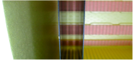
도 8a 및 도 8b는 본 발명의 일 실시예 및 비교예에 따른 세정 과정을 거친 기판을 나타낸 사진이다.
200: 식각 장치 300: 제1 세정 장치
330, 430, 530: 공급부 331, 431, 531: 공급관
332, 432, 532: 노즐 400: 제2 세정 장치
410: 고정 프레임 420: 지지대
440: 이송부 441: 구동축
442: 홈부 443: 롤러
450: 연결관 500: 제3 세정 장치
600: 건조 장치 700: 기판 탈착 장치
841: 제1 공급 챔버 842: 제2 공급 챔버
843: 혼합 챔버 844: 펌프
Claims (17)
- 식각된 기판에 제1 세정액을 제공하는 제1 공급부를 포함하는 제1 세정 장치;
상기 제1 세정액으로 세정된 상기 기판에 제2 세정액을 제공하는 제2 공급부를 포함하는 제2 세정 장치; 및
상기 제2 세정액으로 세정된 상기 기판에 제3 세정액을 제공하는 제3 공급부를 포함하는 제3 세정 장치;
를 포함하고,
상기 제1 세정액 및 상기 제3 세정액은 순수(DI water)이고, 상기 제2 세정액은 알칼리 용액인, 기판의 세정 장치. - 제1항에 있어서,
상기 제2 세정액은 수산화 나트륨과 순수를 혼합하여 형성되는, 기판의 세정 장치. - 제1항에 있어서,
상기 제2 세정액의 산성도는 pH 7 이상 pH 14 이하인, 기판의 세정 장치. - 제1항에 있어서,
상기 제2 세정액을 저장하는 공급 챔버; 및
상기 공급 챔버 및 상기 제2 세정 장치 사이에 배치되어 상기 제2 세정 장치의 상기 제2 공급부에 상기 제2 세정액을 공급하는 펌프;
를 더 포함하는 기판의 세정 장치. - 제4항에 있어서,
상기 공급 챔버는,
수산화물이 저장된 제1 공급 챔버;
순수가 저장된 제2 공급 챔버; 및
상기 제1 공급 챔버 및 상기 제2 공급 챔버에서 각각 공급된 상기 수산화물 및 상기 순수가 혼합된 상기 제2 세정액이 저장된 혼합 챔버;
를 포함하는, 기판의 세정 장치. - 제1항에 있어서,
상기 제1 공급부는 상기 제1 세정액이 공급되는 제1 공급관 및 상기 제1 공급관에 연통되어 상기 기판에 제1 세정액을 분사하는 제1 노즐을 포함하고,
상기 제2 공급부는 상기 제2 세정액이 공급되는 제2 공급관 및 상기 제2 공급관에 연통되어 상기 기판에 상기 제2 세정액을 분사하는 제2 노즐을 포함하고,
상기 제3 공급부는 제3 세정액이 공급되는 제3 공급관 및 상기 제3 공급관에 연통되어 상기 기판에 제3 세정액을 분사하는 제3 노즐을 포함하는, 기판의 세정 장치. - 제1항 내지 제6항 중 어느 한 항에 있어서,
상기 기판을 고정하는 고정 프레임; 및
상기 고정 프레임을 상기 제1 세정 장치, 상기 제2 세정 장치 및 상기 제3 세정 장치로 순차적으로 이송하는 이송부;
를 더 포함하는 기판의 세정 장치. - 제1항에 있어서,
상기 제3 세정 장치에서 상기 제3 세정액으로 세정된 상기 기판을 건조시키기 위해 가스를 제공하는 건조 장치를 더 포함하는 기판의 세정 장치. - 제1항에 있어서,
상기 기판은 각각 글라스로 형성되고 서로 접착된 제1 기판 및 제2 기판을 포함하는, 기판의 세정 장치. - 식각 공정을 거친 기판에 제1 공급부를 통해 제1 세정액을 제공하는 제1 세정 단계;
상기 제1 세정액으로 세정된 상기 기판에 제2 공급부를 통해 제2 세정액을 제공하는 제2 세정 단계; 및
상기 제2 세정액으로 세정된 상기 기판에 제3 공급부를 통해 제3 세정액을 제공하는 제3 세정 단계;
를 포함하고,
상기 제1 세정액 및 상기 제3 세정액은 순수이고, 상기 제2 세정액은 알칼리 용액인, 기판의 세정 방법. - 제10항에 있어서,
상기 제2 세정액은 수산화 나트륨과 순수를 혼합하여 형성하는, 기판의 세정 방법. - 제10항에 있어서,
상기 제2 세정액의 산성도는 pH 7 이상 pH 14 이하인, 기판의 세정 방법. - 제10항에 있어서,
상기 제2 세정액은 혼합 챔버에서 수산화물과 순수를 공급받아 형성하고, 상기 혼합 챔버 및 상기 제2 공급부와 연결된 펌프를 통해 상기 제2 세정액을 상기 제2 공급부에 공급하는, 기판의 세정 방법. - 제10항에 있어서,
상기 제1 공급부, 상기 제2 공급부 및 상기 제3 공급부는 각각 공급관 및 노즐을 포함하고, 상기 제1 세정액, 상기 제2 세정액 및 상기 제3 세정액은 상기 노즐을 통해 상기 기판에 분사되는, 기판의 세정 방법. - 제10항 내지 제14항 중 어느 한 항에 있어서,
상기 기판을 고정 프레임에 고정하고 이송부를 통해 이송하여, 상기 제1 공급부, 상기 제2 공급부 및 상기 제3 공급부에 순차적으로 통과시키는, 기판의 세정 방법. - 제10항에 있어서,
상기 기판을 건조시키기 위해 상기 기판에 가스를 제공하는 건조 단계를 더 포함하는 기판의 세정 방법. - 제10항에 있어서,
상기 기판은 각각 글라스로 형성된 제1 기판 및 제2 기판을 접착하여 형성된, 기판의 세정 방법.
Priority Applications (2)
| Application Number | Priority Date | Filing Date | Title |
|---|---|---|---|
| KR1020100090064A KR20120028079A (ko) | 2010-09-14 | 2010-09-14 | 기판의 세정 장치 및 세정 방법 |
| US13/078,202 US20120060870A1 (en) | 2010-09-14 | 2011-04-01 | Cleansing Apparatus for Substrate and Cleansing Method for the Same |
Applications Claiming Priority (1)
| Application Number | Priority Date | Filing Date | Title |
|---|---|---|---|
| KR1020100090064A KR20120028079A (ko) | 2010-09-14 | 2010-09-14 | 기판의 세정 장치 및 세정 방법 |
Publications (1)
| Publication Number | Publication Date |
|---|---|
| KR20120028079A true KR20120028079A (ko) | 2012-03-22 |
Family
ID=45805466
Family Applications (1)
| Application Number | Title | Priority Date | Filing Date |
|---|---|---|---|
| KR1020100090064A Ceased KR20120028079A (ko) | 2010-09-14 | 2010-09-14 | 기판의 세정 장치 및 세정 방법 |
Country Status (2)
| Country | Link |
|---|---|
| US (1) | US20120060870A1 (ko) |
| KR (1) | KR20120028079A (ko) |
Cited By (1)
| Publication number | Priority date | Publication date | Assignee | Title |
|---|---|---|---|---|
| KR20190019575A (ko) * | 2017-08-18 | 2019-02-27 | 에스케이실트론 주식회사 | 웨이퍼 세정 장치 |
Families Citing this family (2)
| Publication number | Priority date | Publication date | Assignee | Title |
|---|---|---|---|---|
| CN107520159A (zh) * | 2017-08-21 | 2017-12-29 | 深圳市欣裕达机械设备有限公司 | 一种新型高效率直立通过式Tray清洗机 |
| CN108919565A (zh) * | 2018-06-29 | 2018-11-30 | 张家港康得新光电材料有限公司 | 一种导电玻璃的清洗方法 |
Family Cites Families (15)
| Publication number | Priority date | Publication date | Assignee | Title |
|---|---|---|---|---|
| JP2727481B2 (ja) * | 1992-02-07 | 1998-03-11 | キヤノン株式会社 | 液晶素子用ガラス基板の洗浄方法 |
| JPH08126873A (ja) * | 1994-10-28 | 1996-05-21 | Nec Corp | 電子部品等の洗浄方法及び装置 |
| US5762749A (en) * | 1995-07-21 | 1998-06-09 | Dainippon Screen Mfg. Co., Ltd. | Apparatus for removing liquid from substrates |
| JP3590470B2 (ja) * | 1996-03-27 | 2004-11-17 | アルプス電気株式会社 | 洗浄水生成方法および洗浄方法ならびに洗浄水生成装置および洗浄装置 |
| US6350322B1 (en) * | 1997-03-21 | 2002-02-26 | Micron Technology, Inc. | Method of reducing water spotting and oxide growth on a semiconductor structure |
| JPH11121417A (ja) * | 1997-10-09 | 1999-04-30 | Mitsubishi Electric Corp | 半導体基板の処理システムおよび処理方法 |
| TW426874B (en) * | 1998-10-14 | 2001-03-21 | United Microelectronics Corp | Method for cleaning a semiconductor wafer |
| TW466558B (en) * | 1999-09-30 | 2001-12-01 | Purex Co Ltd | Method of removing contamination adhered to surfaces and apparatus used therefor |
| JP3343344B2 (ja) * | 2000-05-30 | 2002-11-11 | ファインマシーンカタオカ株式会社 | 超音波洗浄装置 |
| US6503333B2 (en) * | 2000-11-30 | 2003-01-07 | Taiwan Semiconductor Manufacturing Company, Ltd | Method for cleaning semiconductor wafers with ozone-containing solvent |
| JP2003164816A (ja) * | 2001-11-29 | 2003-06-10 | Fine Machine Kataoka Kk | 洗浄装置と、そのワーク搬送方法 |
| US7276724B2 (en) * | 2005-01-20 | 2007-10-02 | Nanosolar, Inc. | Series interconnected optoelectronic device module assembly |
| JP2006093334A (ja) * | 2004-09-22 | 2006-04-06 | Ses Co Ltd | 基板処理装置 |
| US8015984B2 (en) * | 2005-06-22 | 2011-09-13 | Tokyo Electron Limited | Substrate processing apparatus including a drying mechanism using a fluid mixture of purified water and a volatile organic solvent |
| US7694688B2 (en) * | 2007-01-05 | 2010-04-13 | Applied Materials, Inc. | Wet clean system design |
-
2010
- 2010-09-14 KR KR1020100090064A patent/KR20120028079A/ko not_active Ceased
-
2011
- 2011-04-01 US US13/078,202 patent/US20120060870A1/en not_active Abandoned
Cited By (1)
| Publication number | Priority date | Publication date | Assignee | Title |
|---|---|---|---|---|
| KR20190019575A (ko) * | 2017-08-18 | 2019-02-27 | 에스케이실트론 주식회사 | 웨이퍼 세정 장치 |
Also Published As
| Publication number | Publication date |
|---|---|
| US20120060870A1 (en) | 2012-03-15 |
Similar Documents
| Publication | Publication Date | Title |
|---|---|---|
| CN104813438B (zh) | 半导体硅片的清洗方法和装置 | |
| US8132580B2 (en) | Substrate processing system and substrate cleaning apparatus including a jetting apparatus | |
| TWI421973B (zh) | 基板處理裝置 | |
| US11260429B2 (en) | Substrate treating apparatus and substrate transporting method | |
| KR20120028079A (ko) | 기판의 세정 장치 및 세정 방법 | |
| US20120172273A1 (en) | Wafer washing water and wafer washing method | |
| US6776853B2 (en) | Cleaning method and method for manufacturing liquid crystal device | |
| KR20120053319A (ko) | 기판 세정 시스템 및 세정 방법 | |
| JP2007284345A (ja) | フラットパネルディスプレイ用ガラス板の製造方法及びその装置 | |
| JP2010131485A (ja) | 基板の液切り装置および液切り方法 | |
| US20120037181A1 (en) | Cleaning methods for improved photovoltaic module efficiency | |
| US20070181148A1 (en) | Wafer cleaning apparatus and related method | |
| JP2978806B2 (ja) | 基板の処理方法 | |
| JP5427876B2 (ja) | シリコンからなる半導体ウェハを半導体ウェハの研磨のプロセス直後に洗浄するための方法 | |
| JP2019043796A (ja) | エッチング用回転治具およびそれを用いたエッチング装置 | |
| KR101138278B1 (ko) | 액정표시소자의 세정장치 | |
| KR20160064742A (ko) | 기판 처리 장치 | |
| US20080156360A1 (en) | Horizontal megasonic module for cleaning substrates | |
| CN111341700A (zh) | 一种共用清洗模块、抛光设备及集成电路制造系统 | |
| KR102047896B1 (ko) | 기판 처리 장치, 그리고 기판 처리 장치를 이용한 기판 처리 방법 | |
| KR20090061399A (ko) | Tft-lcd 글라스 에칭방법 | |
| JP2004258368A (ja) | 基板洗浄装置及び基板洗浄方法、並びに電気光学装置の製造方法 | |
| KR101033122B1 (ko) | 액정표시장치의 제조를 위한 기판세정장치 | |
| KR20100005758A (ko) | 반도체 기판의 습식세정장치 | |
| JP2007047353A (ja) | 電気光学装置の製造方法、及び電気光学パネルの洗浄装置 |
Legal Events
| Date | Code | Title | Description |
|---|---|---|---|
| PA0109 | Patent application |
St.27 status event code: A-0-1-A10-A12-nap-PA0109 |
|
| PG1501 | Laying open of application |
St.27 status event code: A-1-1-Q10-Q12-nap-PG1501 |
|
| N231 | Notification of change of applicant | ||
| PN2301 | Change of applicant |
St.27 status event code: A-3-3-R10-R13-asn-PN2301 St.27 status event code: A-3-3-R10-R11-asn-PN2301 |
|
| A201 | Request for examination | ||
| P11-X000 | Amendment of application requested |
St.27 status event code: A-2-2-P10-P11-nap-X000 |
|
| P13-X000 | Application amended |
St.27 status event code: A-2-2-P10-P13-nap-X000 |
|
| PA0201 | Request for examination |
St.27 status event code: A-1-2-D10-D11-exm-PA0201 |
|
| R18-X000 | Changes to party contact information recorded |
St.27 status event code: A-3-3-R10-R18-oth-X000 |
|
| P22-X000 | Classification modified |
St.27 status event code: A-2-2-P10-P22-nap-X000 |
|
| E902 | Notification of reason for refusal | ||
| PE0902 | Notice of grounds for rejection |
St.27 status event code: A-1-2-D10-D21-exm-PE0902 |
|
| E601 | Decision to refuse application | ||
| PE0601 | Decision on rejection of patent |
St.27 status event code: N-2-6-B10-B15-exm-PE0601 |
|
| R18-X000 | Changes to party contact information recorded |
St.27 status event code: A-3-3-R10-R18-oth-X000 |
|
| P22-X000 | Classification modified |
St.27 status event code: A-2-2-P10-P22-nap-X000 |
|
| P22-X000 | Classification modified |
St.27 status event code: A-2-2-P10-P22-nap-X000 |