KR20120032779A - 고효율 발광 다이오드 및 그것을 제조하는 방법 - Google Patents
고효율 발광 다이오드 및 그것을 제조하는 방법 Download PDFInfo
- Publication number
- KR20120032779A KR20120032779A KR1020100094298A KR20100094298A KR20120032779A KR 20120032779 A KR20120032779 A KR 20120032779A KR 1020100094298 A KR1020100094298 A KR 1020100094298A KR 20100094298 A KR20100094298 A KR 20100094298A KR 20120032779 A KR20120032779 A KR 20120032779A
- Authority
- KR
- South Korea
- Prior art keywords
- metal layer
- layer
- support substrate
- semiconductor
- insulating layer
- Prior art date
- Legal status (The legal status is an assumption and is not a legal conclusion. Google has not performed a legal analysis and makes no representation as to the accuracy of the status listed.)
- Granted
Links
- 238000004519 manufacturing process Methods 0.000 title claims abstract description 21
- 229910052751 metal Inorganic materials 0.000 claims abstract description 193
- 239000002184 metal Substances 0.000 claims abstract description 193
- 239000004065 semiconductor Substances 0.000 claims abstract description 151
- 239000000758 substrate Substances 0.000 claims abstract description 144
- 150000001875 compounds Chemical class 0.000 claims abstract description 48
- ZOKXTWBITQBERF-UHFFFAOYSA-N Molybdenum Chemical compound [Mo] ZOKXTWBITQBERF-UHFFFAOYSA-N 0.000 claims abstract description 9
- 229910052750 molybdenum Inorganic materials 0.000 claims abstract description 9
- 239000011733 molybdenum Substances 0.000 claims abstract description 9
- WFKWXMTUELFFGS-UHFFFAOYSA-N tungsten Chemical compound [W] WFKWXMTUELFFGS-UHFFFAOYSA-N 0.000 claims abstract description 9
- 229910052721 tungsten Inorganic materials 0.000 claims abstract description 9
- 239000010937 tungsten Substances 0.000 claims abstract description 9
- 238000000034 method Methods 0.000 claims description 44
- 230000004888 barrier function Effects 0.000 claims description 20
- 239000010949 copper Substances 0.000 claims description 16
- RYGMFSIKBFXOCR-UHFFFAOYSA-N Copper Chemical compound [Cu] RYGMFSIKBFXOCR-UHFFFAOYSA-N 0.000 claims description 8
- 229910052802 copper Inorganic materials 0.000 claims description 8
- 229910052804 chromium Inorganic materials 0.000 claims description 6
- 238000005530 etching Methods 0.000 claims description 6
- 229910052759 nickel Inorganic materials 0.000 claims description 6
- 229910052719 titanium Inorganic materials 0.000 claims description 6
- 229910052697 platinum Inorganic materials 0.000 claims description 5
- 239000010410 layer Substances 0.000 description 276
- 229910052594 sapphire Inorganic materials 0.000 description 6
- 239000010980 sapphire Substances 0.000 description 6
- JMASRVWKEDWRBT-UHFFFAOYSA-N Gallium nitride Chemical compound [Ga]#N JMASRVWKEDWRBT-UHFFFAOYSA-N 0.000 description 5
- 229910002601 GaN Inorganic materials 0.000 description 4
- 239000006185 dispersion Substances 0.000 description 4
- 238000000605 extraction Methods 0.000 description 4
- 239000000463 material Substances 0.000 description 4
- 238000005229 chemical vapour deposition Methods 0.000 description 3
- 238000005520 cutting process Methods 0.000 description 3
- 238000000151 deposition Methods 0.000 description 3
- 238000010438 heat treatment Methods 0.000 description 3
- 150000004767 nitrides Chemical class 0.000 description 3
- 238000007747 plating Methods 0.000 description 3
- 238000003825 pressing Methods 0.000 description 3
- 239000002356 single layer Substances 0.000 description 3
- 229910015363 Au—Sn Inorganic materials 0.000 description 2
- 229910052581 Si3N4 Inorganic materials 0.000 description 2
- 229910004298 SiO 2 Inorganic materials 0.000 description 2
- VYPSYNLAJGMNEJ-UHFFFAOYSA-N Silicium dioxide Chemical compound O=[Si]=O VYPSYNLAJGMNEJ-UHFFFAOYSA-N 0.000 description 2
- 238000007796 conventional method Methods 0.000 description 2
- 238000010586 diagram Methods 0.000 description 2
- 229910052737 gold Inorganic materials 0.000 description 2
- 125000005842 heteroatom Chemical group 0.000 description 2
- 229910052738 indium Inorganic materials 0.000 description 2
- 230000001678 irradiating effect Effects 0.000 description 2
- 238000002955 isolation Methods 0.000 description 2
- 238000001451 molecular beam epitaxy Methods 0.000 description 2
- 238000000926 separation method Methods 0.000 description 2
- HQVNEWCFYHHQES-UHFFFAOYSA-N silicon nitride Chemical compound N12[Si]34N5[Si]62N3[Si]51N64 HQVNEWCFYHHQES-UHFFFAOYSA-N 0.000 description 2
- 229910052814 silicon oxide Inorganic materials 0.000 description 2
- PIGFYZPCRLYGLF-UHFFFAOYSA-N Aluminum nitride Chemical compound [Al]#N PIGFYZPCRLYGLF-UHFFFAOYSA-N 0.000 description 1
- XUIMIQQOPSSXEZ-UHFFFAOYSA-N Silicon Chemical compound [Si] XUIMIQQOPSSXEZ-UHFFFAOYSA-N 0.000 description 1
- 229910010413 TiO 2 Inorganic materials 0.000 description 1
- 229910052782 aluminium Inorganic materials 0.000 description 1
- 230000003139 buffering effect Effects 0.000 description 1
- 239000003638 chemical reducing agent Substances 0.000 description 1
- 238000005253 cladding Methods 0.000 description 1
- PMHQVHHXPFUNSP-UHFFFAOYSA-M copper(1+);methylsulfanylmethane;bromide Chemical compound Br[Cu].CSC PMHQVHHXPFUNSP-UHFFFAOYSA-M 0.000 description 1
- 239000013078 crystal Substances 0.000 description 1
- 230000008021 deposition Effects 0.000 description 1
- 230000002542 deteriorative effect Effects 0.000 description 1
- 238000009792 diffusion process Methods 0.000 description 1
- 238000004070 electrodeposition Methods 0.000 description 1
- 238000007772 electroless plating Methods 0.000 description 1
- 238000000313 electron-beam-induced deposition Methods 0.000 description 1
- 238000009713 electroplating Methods 0.000 description 1
- 230000005496 eutectics Effects 0.000 description 1
- 229910052733 gallium Inorganic materials 0.000 description 1
- 230000017525 heat dissipation Effects 0.000 description 1
- APFVFJFRJDLVQX-UHFFFAOYSA-N indium atom Chemical compound [In] APFVFJFRJDLVQX-UHFFFAOYSA-N 0.000 description 1
- 239000011810 insulating material Substances 0.000 description 1
- 239000012212 insulator Substances 0.000 description 1
- 239000007769 metal material Substances 0.000 description 1
- 230000003287 optical effect Effects 0.000 description 1
- 238000000059 patterning Methods 0.000 description 1
- 229920002120 photoresistant polymer Polymers 0.000 description 1
- 238000007517 polishing process Methods 0.000 description 1
- 229920000642 polymer Polymers 0.000 description 1
- 230000035939 shock Effects 0.000 description 1
- 229910052710 silicon Inorganic materials 0.000 description 1
- 239000010703 silicon Substances 0.000 description 1
- HBMJWWWQQXIZIP-UHFFFAOYSA-N silicon carbide Chemical compound [Si+]#[C-] HBMJWWWQQXIZIP-UHFFFAOYSA-N 0.000 description 1
- 229910010271 silicon carbide Inorganic materials 0.000 description 1
- 238000004544 sputter deposition Methods 0.000 description 1
- 239000000126 substance Substances 0.000 description 1
- 230000007704 transition Effects 0.000 description 1
Images


Classifications
-
- H—ELECTRICITY
- H10—SEMICONDUCTOR DEVICES; ELECTRIC SOLID-STATE DEVICES NOT OTHERWISE PROVIDED FOR
- H10H—INORGANIC LIGHT-EMITTING SEMICONDUCTOR DEVICES HAVING POTENTIAL BARRIERS
- H10H20/00—Individual inorganic light-emitting semiconductor devices having potential barriers, e.g. light-emitting diodes [LED]
- H10H20/80—Constructional details
- H10H20/81—Bodies
- H10H20/814—Bodies having reflecting means, e.g. semiconductor Bragg reflectors
-
- H—ELECTRICITY
- H10—SEMICONDUCTOR DEVICES; ELECTRIC SOLID-STATE DEVICES NOT OTHERWISE PROVIDED FOR
- H10H—INORGANIC LIGHT-EMITTING SEMICONDUCTOR DEVICES HAVING POTENTIAL BARRIERS
- H10H20/00—Individual inorganic light-emitting semiconductor devices having potential barriers, e.g. light-emitting diodes [LED]
- H10H20/01—Manufacture or treatment
-
- H—ELECTRICITY
- H10—SEMICONDUCTOR DEVICES; ELECTRIC SOLID-STATE DEVICES NOT OTHERWISE PROVIDED FOR
- H10H—INORGANIC LIGHT-EMITTING SEMICONDUCTOR DEVICES HAVING POTENTIAL BARRIERS
- H10H20/00—Individual inorganic light-emitting semiconductor devices having potential barriers, e.g. light-emitting diodes [LED]
- H10H20/80—Constructional details
- H10H20/81—Bodies
- H10H20/819—Bodies characterised by their shape, e.g. curved or truncated substrates
- H10H20/82—Roughened surfaces, e.g. at the interface between epitaxial layers
-
- H—ELECTRICITY
- H10—SEMICONDUCTOR DEVICES; ELECTRIC SOLID-STATE DEVICES NOT OTHERWISE PROVIDED FOR
- H10H—INORGANIC LIGHT-EMITTING SEMICONDUCTOR DEVICES HAVING POTENTIAL BARRIERS
- H10H20/00—Individual inorganic light-emitting semiconductor devices having potential barriers, e.g. light-emitting diodes [LED]
- H10H20/80—Constructional details
- H10H20/83—Electrodes
- H10H20/831—Electrodes characterised by their shape
- H10H20/8312—Electrodes characterised by their shape extending at least partially through the bodies
Landscapes
- Led Devices (AREA)
Abstract
Description
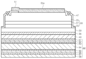
도 6은 본 발명의 일 실시예에 따른 발광 다이오드를 설명하기 위한 개략적인 레이아웃도이다.
도 7은 본 발명의 일 실시예에 따른 발광 다이오드를 설명하기 위해 도 1의 절취선 A-A를 따라 취해진 단면도이다.
도 8은 본 발명의 일 실시예에 따른 발광 다이오드를 설명하기 위해 도 1의 절취선 B-B를 따라 취해진 단면도이다.
도 9는 본 발명의 일 실시예에 따른 발광 다이오드를 설명하기 위해 도 1의 절취선 C-C를 따라 취해진 단면도이다.
도 10 내지 도 14는 본 발명의 일 실시예에 따른 발광 다이오드를 제조하는 방법을 설명하기 위한 단면도들로서, 각각 도 6의 절취선 A-A에 대응하는 단면도들이다.
Claims (21)
- 도전성의 지지기판;
상기 지지기판 상에 위치하고, p형 화합물 반도체층, 활성층 및 n형 화합물 반도체층을 포함하는 반도체 적층 구조체; 및
상기 지지기판과 상기 반도체 적층 구조체 사이에 개재된 본딩 메탈을 포함하되;
상기 지지기판은,
텅스텐(W) 또는 몰리브덴(Mo)중 적어도 하나를 포함하는 제1 금속층;
상기 제1 금속층보다 열팽창 계수가 높으며, 상기 제1 금속층의 상하면에 대칭 구조로 배치되는 제2 금속층을 포함하며;
상기 제1 금속층 및 상기 제2 금속층사이에 접합층이 형성된 것을 특징으로 하는 발광 다이오드. - 청구항 1에 있어서,
상기 제2 금속층은 구리(Cu)를 포함하는 발광 다이오드. - 청구항 1에 있어서,
상기 접합층은 Ni, Ti, Cr, Pt 중 중 적어도 하나를 포함하는 발광 다이오드. - 청구항 1에 있어서,
상기 지지기판과 상기 반도체 적층 구조체 사이에 개재된 상기 본딩 메탈에 대칭하여, 상기 제2 금속층의 하면에 형성된 하부 본딩 메탈을 더 포함하는 발광 다이오드. - 청구항 1에 있어서,
상기 지지기판과 상기 반도체 적층 구조체 사이에 위치하여 상기 반도체 적층 구조체에 오믹 콘택하고, 상기 반도체 적층 구조체를 노출시키는 홈을 갖는 반사 금속층;
상기 반사 금속층과 상기 지지기판 사이에 위치하고 상기 홈을 채움과 아울러 상기 반사 금속층을 덮되, 상기 반사 금속층을 노출시키는 개구부들을 갖는 중간 절연층;
상기 지지기판과 상기 중간 절연층 사이에 위치하고 상기 중간 절연층의 개구부들에 노출된 상기 반사 금속층을 덮는 장벽 금속층;
상기 반도체 적층 구조체 상에 위치하는 제1 전극 패드;
상기 제1 전극 패드에서 연장하는 전극 연장부; 및
상기 제1 전극 패드와 상기 반도체 적층 구조체 사이에 개재된 상부 절연층을 더 포함하는 발광 다이오드. - 청구항 5에 있어서,
상기 제1 전극 패드 및 상기 전극 연장부는 상기 홈 영역 상부에 위치하는 발광 다이오드. - 청구항 5에 있어서,
상기 반사 금속층은 복수개의 판(plate)으로 이루어지고, 상기 중간 절연층은 상기 복수개의 판들의 측면 및 가장자리를 덮으며, 상기 중간 절연층의 개구부들에 의해 상기 복수개의 판들이 각각 노출되는 발광 다이오드. - 청구항 7에 있어서,
복수개의 제1 전극 패드; 및
상기 복수개의 제1 전극 패드에서 각각 연장하는 복수개의 전극 연장부들을 포함하되,
상기 복수개의 제1 전극 패드 및 전극 연장부들은 상기 복수개의 판들 사이의 영역 상부에 위치하는 발광 다이오드. - 청구항 5에 있어서,
상기 반도체 적층 구조체는 거칠어진 표면을 갖고,
상기 상부 절연층은 상기 거칠어진 표면을 덮되,
상기 상부 절연층은 상기 거칠어진 표면을 따라 요철면을 형성하는 발광 다이오드. - 청구항 9에 있어서,
상기 반도체 적층 구조체는 평평한 표면을 갖고, 상기 제1 전극 패드 및 상기 전극 연장부는 상기 평평한 표면 상에 위치하는 발광 다이오드. - 청구항 10에 있어서,
상기 전극 연장부는 상기 반도체 적층 구조체의 평평한 표면에 접촉하는 발광 다이오드. - 청구항 9에 있어서,
상기 거칠어진 표면은 상기 전극 연장부보다 아래에 위치하는 발광 다이오드. - 성장 기판 상에 p형 화합물 반도체층, 활성층 및 n형 화합물 반도체층을 포함하는 반도체 적층 구조체를 형성하고,
상기 적층 구조체에 본딩 메탈을 개재하여 도전성의 지지 기판을 부착하고,
상기 성장 기판을 제거하여 상기 반도체 적층 구조체를 노출시키되,
상기 지지기판은,
텅스텐(W) 또는 몰리브덴(Mo)중 적어도 하나를 포함하는 제1 금속층;
상기 제1 금속층보다 열팽창 계수가 높으며, 상기 제1 금속층의 상하면에 대칭되어 배치되는 제2 금속층을 포함하며;
상기 제1 금속층 및 상기 제2 금속층사이에 접합층이 형성된 것을 특징으로 하는 발광 다이오드 제조 방법. - 청구항 13에 있어서,
상기 제2 금속층은 구리(Cu)를 포함하는 발광 다이오드 제조 방법. - 청구항 13에 있어서,
상기 접합층은 Ni, Ti, Cr, Pt 중 중 적어도 하나를 포함하는 발광 다이오드 제조 방법. - 청구항 13에 있어서,
상기 지지기판과 상기 반도체 적층 구조체 사이에 개재된 본딩 메탈에 대칭하여, 상기 제2 금속층의 하면에 형성된 하부 본딩 메탈을 더 포함하는 발광 다이오드 제조 방법. - 청구항 13에 있어서,
상기 반도체 적층 구조체상에 상기 지지 기판을 부착하기 전에,
상기 반도체 적층 구조체 상에 반사 금속층을 형성하되, 상기 반사 금속층은 상기 반도체 적층 구조체를 노출시키는 홈을 갖고,
상기 반사금속층을 덮는 중간 절연층을 형성하되, 상기 중간 절연층은 상기 반사 금속층의 측면 및 가장자리를 덮으며, 또한 상기 반사 금속층을 노출시키는 개구부를 갖고,
상기 중간 절연층의 개구부를 통해 상기 반사 금속층에 접속하는 장벽 금속층을 형성하고,
상기 장벽 금속층 상에 지지기판을 부착하고,
상기 성장 기판을 제거하여 상기 반도체 적층 구조체를 노출시킨 후에,
상기 노출된 반도체 적층 구조체 상에 마스크 패턴을 형성하고,
상기 마스크 패턴을 식각 마스크로 사용하여 상기 반도체 적층 구조체의 표면을 이방성 식각함으로써 평평한 표면과 함께 거칠어진 표면을 형성하고,
상기 반도체 적층 구조체의 표면을 덮는 상부 절연층을 형성하되, 상기 상부 절연층은 상기 평평한 표면의 일부 영역을 노출시키는 개구부를 갖고,
상기 상부 절연층 상에 제1 전극 패드를 형성함과 아울러, 상기 제1 전극 패드로부터 연장하는 전극 연장부를 형성하되, 상기 전극 연장부는 상기 상부 절연층의 개구부 내에 형성되는 발광 다이오드 제조 방법. - 청구항 17에 있어서,
상기 제1 전극 패드 및 상기 전극 연장부는 상기 반사 금속층의 홈 영역 상부에 형성되는 발광 다이오드 제조 방법. - 청구항 17에 있어서,
상기 반사 금속층은 복수개의 판(plate)으로 형성되고, 상기 중간 절연층은 상기 복수개의 판들의 측면 및 가장자리를 덮으며, 상기 중간 절연층의 개구부들에 의해 상기 복수개의 판들이 각각 노출되는 발광 다이오드 제조 방법. - 청구항 19에 있어서,
복수개의 제1 전극 패드 및 복수개의 전극 연장부들이 각각 상기 복수개의 판들 사이의 영역 상부에 형성되는 발광 다이오드 제조 방법. - 청구항 17에 있어서,
상기 상부 절연층은 상기 거치어진 표면을 따라 형성되어 요철면을 갖는 발광 다이오드 제조 방법.
Priority Applications (11)
| Application Number | Priority Date | Filing Date | Title |
|---|---|---|---|
| KR1020100094298A KR101158077B1 (ko) | 2010-09-29 | 2010-09-29 | 고효율 발광 다이오드 및 그것을 제조하는 방법 |
| JP2011072531A JP5725927B2 (ja) | 2010-05-18 | 2011-03-29 | 高効率発光ダイオード及びその製造方法 |
| PCT/KR2011/003592 WO2011145850A2 (en) | 2010-05-18 | 2011-05-16 | High efficiency light emitting diode and method of fabricating the same |
| TW104118511A TWI546983B (zh) | 2010-05-18 | 2011-05-17 | 高效率發光二極體 |
| TW100117223A TWI493757B (zh) | 2010-05-18 | 2011-05-17 | 高效率發光二極體 |
| EP11166366.2A EP2388836B1 (en) | 2010-05-18 | 2011-05-17 | High-efficiency light-emitting diode and method of fabricating the same |
| US13/109,669 US9029888B2 (en) | 2010-05-18 | 2011-05-17 | High efficiency light emitting diode and method of fabricating the same |
| CN201110140245.0A CN102255022B (zh) | 2010-05-18 | 2011-05-18 | 高效发光二极管 |
| CN201610286085.3A CN105895770B (zh) | 2010-05-18 | 2011-05-18 | 发光二极管 |
| CN201510229202.8A CN104851952B (zh) | 2010-05-18 | 2011-05-18 | 高效发光二极管 |
| US14/694,651 US10249797B2 (en) | 2010-05-18 | 2015-04-23 | High efficiency light emitting diode and method of fabricating the same |
Applications Claiming Priority (1)
| Application Number | Priority Date | Filing Date | Title |
|---|---|---|---|
| KR1020100094298A KR101158077B1 (ko) | 2010-09-29 | 2010-09-29 | 고효율 발광 다이오드 및 그것을 제조하는 방법 |
Related Child Applications (1)
| Application Number | Title | Priority Date | Filing Date |
|---|---|---|---|
| KR1020110141125A Division KR20120033294A (ko) | 2011-12-23 | 2011-12-23 | 고효율 발광 다이오드 및 그것을 제조하는 방법 |
Publications (2)
| Publication Number | Publication Date |
|---|---|
| KR20120032779A true KR20120032779A (ko) | 2012-04-06 |
| KR101158077B1 KR101158077B1 (ko) | 2012-06-22 |
Family
ID=46135712
Family Applications (1)
| Application Number | Title | Priority Date | Filing Date |
|---|---|---|---|
| KR1020100094298A Active KR101158077B1 (ko) | 2010-05-18 | 2010-09-29 | 고효율 발광 다이오드 및 그것을 제조하는 방법 |
Country Status (1)
| Country | Link |
|---|---|
| KR (1) | KR101158077B1 (ko) |
Cited By (2)
| Publication number | Priority date | Publication date | Assignee | Title |
|---|---|---|---|---|
| CN118213326A (zh) * | 2024-05-20 | 2024-06-18 | 扬州扬杰电子科技股份有限公司 | 一种二极管叠片及其制备方法 |
| CN120239374A (zh) * | 2024-03-19 | 2025-07-01 | 原子能与替代能源委员会 | 制造光电子器件的方法 |
Family Cites Families (3)
| Publication number | Priority date | Publication date | Assignee | Title |
|---|---|---|---|---|
| KR100872276B1 (ko) * | 2006-11-27 | 2008-12-05 | 삼성전기주식회사 | 수직구조 질화물 반도체 발광 소자 및 제조방법 |
| JP5334158B2 (ja) | 2008-07-15 | 2013-11-06 | シャープ株式会社 | 窒化物半導体発光素子および窒化物半導体発光素子の製造方法 |
| KR100999548B1 (ko) * | 2008-11-24 | 2010-12-08 | 고려대학교 산학협력단 | 수직구조를 갖는 반도체 발광소자 제조용 지지기판, 이를 이용한 수직구조를 갖는 반도체 발광소자 제조방법 및 수직구조를 갖는 반도체 발광소자 |
-
2010
- 2010-09-29 KR KR1020100094298A patent/KR101158077B1/ko active Active
Cited By (2)
| Publication number | Priority date | Publication date | Assignee | Title |
|---|---|---|---|---|
| CN120239374A (zh) * | 2024-03-19 | 2025-07-01 | 原子能与替代能源委员会 | 制造光电子器件的方法 |
| CN118213326A (zh) * | 2024-05-20 | 2024-06-18 | 扬州扬杰电子科技股份有限公司 | 一种二极管叠片及其制备方法 |
Also Published As
| Publication number | Publication date |
|---|---|
| KR101158077B1 (ko) | 2012-06-22 |
Similar Documents
| Publication | Publication Date | Title |
|---|---|---|
| CN105895770B (zh) | 发光二极管 | |
| KR101017394B1 (ko) | 발광 소자 및 그것을 제조하는 방법 | |
| JP2009283984A (ja) | フリップチップ発光ダイオード及びその製造方法 | |
| KR20100035846A (ko) | 발광 소자 및 그 제조방법 | |
| JP6410870B2 (ja) | 発光ダイオード | |
| US12002842B2 (en) | Light emitting device and manufacturing method thereof | |
| KR101154511B1 (ko) | 고효율 발광 다이오드 및 그것을 제조하는 방법 | |
| KR101769072B1 (ko) | 고효율 발광 다이오드 및 그것을 제조하는 방법 | |
| KR101364167B1 (ko) | 수직형 발광 다이오드 및 그 제조방법 | |
| KR101158077B1 (ko) | 고효율 발광 다이오드 및 그것을 제조하는 방법 | |
| KR101773582B1 (ko) | 고효율 발광 다이오드 | |
| KR20090115902A (ko) | 수직구조 그룹 3족 질화물계 반도체 발광다이오드 소자 및제조방법 | |
| KR101316121B1 (ko) | 수직형 발광 다이오드의 제조방법 | |
| KR101239849B1 (ko) | 고효율 발광 다이오드 | |
| KR101138978B1 (ko) | 고효율 발광 다이오드 및 그것을 제조하는 방법 | |
| KR101171855B1 (ko) | 반도체 발광소자용 지지기판 및 상기 지지기판을 이용한고성능 수직구조의 반도체 발광소자 | |
| KR101634370B1 (ko) | 고효율 발광 다이오드 및 그것을 제조하는 방법 | |
| KR20120033294A (ko) | 고효율 발광 다이오드 및 그것을 제조하는 방법 | |
| KR20120073396A (ko) | 발광 다이오드 및 그의 제조 방법 | |
| KR20100006224A (ko) | 발광 소자 및 그 제조방법 | |
| KR101681573B1 (ko) | 발광소자의 제조방법 | |
| KR101337613B1 (ko) | 발광소자와 그 제조방법 | |
| KR20120117528A (ko) | 수직형 led 소자 및 그 제조 방법 | |
| KR20090104576A (ko) | 수직형 발광 소자 및 그 제조방법 |
Legal Events
| Date | Code | Title | Description |
|---|---|---|---|
| A201 | Request for examination | ||
| PA0109 | Patent application |
Patent event code: PA01091R01D Comment text: Patent Application Patent event date: 20100929 |
|
| PA0201 | Request for examination | ||
| PE0902 | Notice of grounds for rejection |
Comment text: Notification of reason for refusal Patent event date: 20111028 Patent event code: PE09021S01D |
|
| A107 | Divisional application of patent | ||
| PA0107 | Divisional application |
Comment text: Divisional Application of Patent Patent event date: 20111223 Patent event code: PA01071R01D |
|
| E701 | Decision to grant or registration of patent right | ||
| PE0701 | Decision of registration |
Patent event code: PE07011S01D Comment text: Decision to Grant Registration Patent event date: 20120330 |
|
| PG1501 | Laying open of application | ||
| GRNT | Written decision to grant | ||
| PR0701 | Registration of establishment |
Comment text: Registration of Establishment Patent event date: 20120613 Patent event code: PR07011E01D |
|
| PR1002 | Payment of registration fee |
Payment date: 20120614 End annual number: 3 Start annual number: 1 |
|
| PG1601 | Publication of registration | ||
| FPAY | Annual fee payment |
Payment date: 20150401 Year of fee payment: 4 |
|
| PR1001 | Payment of annual fee |
Payment date: 20150401 Start annual number: 4 End annual number: 4 |
|
| FPAY | Annual fee payment |
Payment date: 20170308 Year of fee payment: 6 |
|
| PR1001 | Payment of annual fee |
Payment date: 20170308 Start annual number: 6 End annual number: 6 |
|
| FPAY | Annual fee payment |
Payment date: 20190325 Year of fee payment: 8 |
|
| PR1001 | Payment of annual fee |
Payment date: 20190325 Start annual number: 8 End annual number: 8 |
|
| PR1001 | Payment of annual fee |
Payment date: 20200401 Start annual number: 9 End annual number: 9 |
|
| PR1001 | Payment of annual fee |
Payment date: 20210407 Start annual number: 10 End annual number: 10 |
|
| PR1001 | Payment of annual fee |
Payment date: 20220329 Start annual number: 11 End annual number: 11 |
|
| PR1001 | Payment of annual fee |
Payment date: 20240326 Start annual number: 13 End annual number: 13 |