KR20120122549A - 반도체 메모리 장치 및 그의 리페어 방법 - Google Patents
반도체 메모리 장치 및 그의 리페어 방법 Download PDFInfo
- Publication number
- KR20120122549A KR20120122549A KR20110040776A KR20110040776A KR20120122549A KR 20120122549 A KR20120122549 A KR 20120122549A KR 20110040776 A KR20110040776 A KR 20110040776A KR 20110040776 A KR20110040776 A KR 20110040776A KR 20120122549 A KR20120122549 A KR 20120122549A
- Authority
- KR
- South Korea
- Prior art keywords
- memory
- semiconductor
- memory cells
- chip
- cells
- Prior art date
- Legal status (The legal status is an assumption and is not a legal conclusion. Google has not performed a legal analysis and makes no representation as to the accuracy of the status listed.)
- Ceased
Links
Images


Classifications
-
- G—PHYSICS
- G11—INFORMATION STORAGE
- G11C—STATIC STORES
- G11C29/00—Checking stores for correct operation ; Subsequent repair; Testing stores during standby or offline operation
- G11C29/04—Detection or location of defective memory elements, e.g. cell constructio details, timing of test signals
-
- H—ELECTRICITY
- H10—SEMICONDUCTOR DEVICES; ELECTRIC SOLID-STATE DEVICES NOT OTHERWISE PROVIDED FOR
- H10W—GENERIC PACKAGES, INTERCONNECTIONS, CONNECTORS OR OTHER CONSTRUCTIONAL DETAILS OF DEVICES COVERED BY CLASS H10
- H10W90/00—Package configurations
-
- G—PHYSICS
- G11—INFORMATION STORAGE
- G11C—STATIC STORES
- G11C29/00—Checking stores for correct operation ; Subsequent repair; Testing stores during standby or offline operation
- G11C29/70—Masking faults in memories by using spares or by reconfiguring
- G11C29/78—Masking faults in memories by using spares or by reconfiguring using programmable devices
- G11C29/785—Masking faults in memories by using spares or by reconfiguring using programmable devices with redundancy programming schemes
-
- G—PHYSICS
- G11—INFORMATION STORAGE
- G11C—STATIC STORES
- G11C29/00—Checking stores for correct operation ; Subsequent repair; Testing stores during standby or offline operation
- G11C29/70—Masking faults in memories by using spares or by reconfiguring
- G11C29/78—Masking faults in memories by using spares or by reconfiguring using programmable devices
- G11C29/80—Masking faults in memories by using spares or by reconfiguring using programmable devices with improved layout
- G11C29/81—Masking faults in memories by using spares or by reconfiguring using programmable devices with improved layout using a hierarchical redundancy scheme
-
- H—ELECTRICITY
- H10—SEMICONDUCTOR DEVICES; ELECTRIC SOLID-STATE DEVICES NOT OTHERWISE PROVIDED FOR
- H10B—ELECTRONIC MEMORY DEVICES
- H10B20/00—Read-only memory [ROM] devices
- H10B20/20—Programmable ROM [PROM] devices comprising field-effect components
-
- H—ELECTRICITY
- H10—SEMICONDUCTOR DEVICES; ELECTRIC SOLID-STATE DEVICES NOT OTHERWISE PROVIDED FOR
- H10W—GENERIC PACKAGES, INTERCONNECTIONS, CONNECTORS OR OTHER CONSTRUCTIONAL DETAILS OF DEVICES COVERED BY CLASS H10
- H10W20/00—Interconnections in chips, wafers or substrates
- H10W20/40—Interconnections external to wafers or substrates, e.g. back-end-of-line [BEOL] metallisations or vias connecting to gate electrodes
- H10W20/49—Adaptable interconnections, e.g. fuses or antifuses
- H10W20/493—Fuses, i.e. interconnections changeable from conductive to non-conductive
-
- H—ELECTRICITY
- H10—SEMICONDUCTOR DEVICES; ELECTRIC SOLID-STATE DEVICES NOT OTHERWISE PROVIDED FOR
- H10W—GENERIC PACKAGES, INTERCONNECTIONS, CONNECTORS OR OTHER CONSTRUCTIONAL DETAILS OF DEVICES COVERED BY CLASS H10
- H10W90/00—Package configurations
- H10W90/20—Configurations of stacked chips
- H10W90/284—Configurations of stacked chips characterised by structural arrangements for measuring or testing
Landscapes
- For Increasing The Reliability Of Semiconductor Memories (AREA)
- Semiconductor Memories (AREA)
Abstract
Description
도 2는 종래기술에 따른 반도체 메모리 장치의 리페어 방법을 설명하기 위한 흐름도.
도 3은 본 발명의 제1 실시예에 따른 반도체 메모리 장치의 블록 구성도.
도 4는 본 발명의 제2 실시예에 따른 반도체 메모리 장치의 블록 구성도.
도 5는 도 3 및 도 4에 도시된 반도체 메모리 장치에 적용될 수 있는 리페어 방법의 일예를 보인 흐름도.
도 6은 도 3 및 도 4에 도시된 반도체 메모리 장치에 적용될 수 있는 리페어 방법의 다른 예를 보인 흐름도.
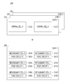
212A, 212B : 다수의 메모리 셀 220 : 제2 메모리 칩
222A, 222B : 다수의 메모리 셀 230 : 제3 메모리 칩
232A, 232B : 다수의 메모리 셀 240 : 리페어 칩
241A, 241B : 제1 퓨즈회로 242A, 242B : 제1 리던던시 셀
243A, 243B : 제2 퓨즈회로 244A, 244B : 제2 리던던시 셀
245A, 245B : 제3 퓨즈회로 246A, 246B : 제3 리던던시 셀
Claims (12)
- 다수의 메모리 셀을 포함하는 적어도 하나 이상의 제1 반도체 칩; 및
상기 적어도 하나 이상의 제1 반도체 칩에 포함된 상기 다수의 메모리 셀 중에서 결함이 발생한 임의의 메모리 셀들을 리페어하기 위한 퓨즈회로를 포함하는 제2 반도체 칩
을 구비하는 반도체 메모리 장치.
- 제1항에 있어서,
상기 적어도 하나 이상의 제1 반도체 칩과 상기 제2 반도체 칩은 수직으로 스택되는 반도체 메모리 장치.
- 제2항에 있어서,
상기 적어도 하나 이상의 제1 반도체 칩은 상기 결함이 발생한 임의의 메모리 셀들을 대체하기 위한 다수의 리던던시 메모리 셀을 더 포함하는 반도체 메모리 장치.
- 제2항에 있어서,
상기 제2 반도체 칩은 상기 적어도 하나 이상의 제1 반도체 칩에 대응하여 상기 결함이 발생한 임의의 메모리 셀들을 대체하기 위한 다수의 리던던시 메모리 셀을 더 포함하는 반도체 메모리 장치.
- 제1항 내지 제4항 중 어느 한 항에 있어서,
상기 제2 반도체 칩은 상기 적어도 하나 이상의 제1 반도체 칩을 제어하기 위한 마스터 칩이고,
상기 적어도 하나 이상의 제1 반도체 칩은 상기 제2 반도체 칩의 제어를 받는 슬레이브 칩인 반도체 메모리 장치.
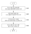
- 다수의 메모리 셀과 상기 다수의 메모리 셀 중 결함이 발생한 메모리 셀들을 리페어하기 위한 퓨즈회로가 서로 다른 반도체 칩에 분리되어 배치된 반도체 메모리 장치의 리페어 방법에 있어서,
다수의 제1 반도체 칩 각각에 포함된 상기 다수의 메모리 셀을 테스트하는 단계; 및
상기 다수의 제1 반도체 칩의 통합된 테스트 결과에 따라 제2 반도체 칩에 포함된 상기 퓨즈회로를 프로그램하는 단계
를 포함하는 반도체 메모리 장치의 리페어 방법.
- 제6항에 있어서,
상기 통합된 테스트 결과를 기억하는 단계를 더 포함하는 반도체 메모리 장치의 리페어 방법.
- 제6항 또는 제7항에 있어서,
상기 테스트하는 단계는 웨이퍼 레벨의 테스트를 실시하는 반도체 메모리 장치의 리페어 방법.
- 제6항 또는 제7항에 있어서,
상기 퓨즈회로를 프로그램하는 단계 이후에 상기 다수의 제1 반도체 칩과 제2 반도체 칩을 수직으로 스택하는 단계를 더 포함하는 반도체 메모리 장치의 리페어 방법.
- 다수의 메모리 셀과 상기 다수의 메모리 셀 중 결함이 발생한 메모리 셀들을 리페어하기 위한 퓨즈회로가 서로 다른 반도체 칩에 분리되어 배치된 반도체 메모리 장치의 리페어 방법에 있어서,
상기 다수의 메모리 셀을 각각 포함하는 다수의 제1 반도체 칩을 수직으로 스택하는 단계;
스택된 상기 다수의 제1 반도체 칩 각각에 포함된 상기 다수의 메모리 셀을 테스트하는 단계; 및
상기 다수의 제1 반도체 칩의 통합된 테스트 결과에 따라 제2 반도체 칩에 포함된 상기 퓨즈회로를 프로그램하는 단계
를 포함하는 반도체 메모리 장치의 리페어 방법.
- 제10항에 있어서,
상기 통합된 테스트 결과를 기억하는 단계를 더 포함하는 반도체 메모리 장치의 리페어 방법.
- 제10항 또는 제11항에 있어서,
상기 퓨즈회로를 프로그램하는 단계 이후에 상기 스택된 다수의 제1 메모리 칩과 제2 반도체 칩을 수직으로 스택하는 단계를 더 포함하는 반도체 메모리 장치의 리페어 방법.
Priority Applications (3)
| Application Number | Priority Date | Filing Date | Title |
|---|---|---|---|
| KR20110040776A KR20120122549A (ko) | 2011-04-29 | 2011-04-29 | 반도체 메모리 장치 및 그의 리페어 방법 |
| US13/205,780 US8848443B2 (en) | 2011-04-29 | 2011-08-09 | Semiconductor memory device and repair method thereof |
| JP2011185467A JP5892747B2 (ja) | 2011-04-29 | 2011-08-29 | 半導体メモリ装置及びそのリペア方法 |
Applications Claiming Priority (1)
| Application Number | Priority Date | Filing Date | Title |
|---|---|---|---|
| KR20110040776A KR20120122549A (ko) | 2011-04-29 | 2011-04-29 | 반도체 메모리 장치 및 그의 리페어 방법 |
Publications (1)
| Publication Number | Publication Date |
|---|---|
| KR20120122549A true KR20120122549A (ko) | 2012-11-07 |
Family
ID=47067236
Family Applications (1)
| Application Number | Title | Priority Date | Filing Date |
|---|---|---|---|
| KR20110040776A Ceased KR20120122549A (ko) | 2011-04-29 | 2011-04-29 | 반도체 메모리 장치 및 그의 리페어 방법 |
Country Status (3)
| Country | Link |
|---|---|
| US (1) | US8848443B2 (ko) |
| JP (1) | JP5892747B2 (ko) |
| KR (1) | KR20120122549A (ko) |
Cited By (1)
| Publication number | Priority date | Publication date | Assignee | Title |
|---|---|---|---|---|
| US10553635B2 (en) | 2015-09-25 | 2020-02-04 | Samsung Electronics Co., Ltd. | Image sensor, stacked image sensor, image processing apparatus, and method of fabricating image sensor chip package |
Families Citing this family (11)
| Publication number | Priority date | Publication date | Assignee | Title |
|---|---|---|---|---|
| US10314594B2 (en) | 2012-12-14 | 2019-06-11 | Corquest Medical, Inc. | Assembly and method for left atrial appendage occlusion |
| US10307167B2 (en) | 2012-12-14 | 2019-06-04 | Corquest Medical, Inc. | Assembly and method for left atrial appendage occlusion |
| US10813630B2 (en) | 2011-08-09 | 2020-10-27 | Corquest Medical, Inc. | Closure system for atrial wall |
| US9472284B2 (en) | 2012-11-19 | 2016-10-18 | Silicon Storage Technology, Inc. | Three-dimensional flash memory system |
| US20140142689A1 (en) | 2012-11-21 | 2014-05-22 | Didier De Canniere | Device and method of treating heart valve malfunction |
| US9566443B2 (en) | 2013-11-26 | 2017-02-14 | Corquest Medical, Inc. | System for treating heart valve malfunction including mitral regurgitation |
| US10842626B2 (en) | 2014-12-09 | 2020-11-24 | Didier De Canniere | Intracardiac device to correct mitral regurgitation |
| JP2017033612A (ja) * | 2015-07-29 | 2017-02-09 | 淳生 越塚 | 半導体記憶装置及びその制御方法 |
| CN106548809A (zh) | 2015-09-22 | 2017-03-29 | 飞思卡尔半导体公司 | 处理缺陷非易失性存储器 |
| US10636767B2 (en) * | 2016-02-29 | 2020-04-28 | Invensas Corporation | Correction die for wafer/die stack |
| CN108735268B (zh) | 2017-04-19 | 2024-01-30 | 恩智浦美国有限公司 | 非易失性存储器修复电路 |
Family Cites Families (19)
| Publication number | Priority date | Publication date | Assignee | Title |
|---|---|---|---|---|
| US4376300A (en) * | 1981-01-02 | 1983-03-08 | Intel Corporation | Memory system employing mostly good memories |
| US5502333A (en) * | 1994-03-30 | 1996-03-26 | International Business Machines Corporation | Semiconductor stack structures and fabrication/sparing methods utilizing programmable spare circuit |
| JPH0816486A (ja) * | 1994-06-29 | 1996-01-19 | Hitachi Ltd | 欠陥救済用lsiとメモリ装置 |
| US5644541A (en) * | 1995-11-03 | 1997-07-01 | Philip K. Siu | Memory substitution system and method for correcting partially defective memories |
| JPH10289595A (ja) * | 1997-04-14 | 1998-10-27 | Matsushita Electric Ind Co Ltd | 半導体メモリ装置およびその製造方法 |
| JPH1196081A (ja) * | 1997-09-22 | 1999-04-09 | Chishiki Joho Kenkyusho:Kk | 記憶装置の制御方法および記憶装置ならびに記憶装置の製造方法 |
| KR20000060983A (ko) | 1999-03-22 | 2000-10-16 | 김영환 | 메모리소자의 리던던시셀 |
| JP2003036692A (ja) * | 2001-07-24 | 2003-02-07 | Matsushita Electric Ind Co Ltd | 不揮発性半導体記憶装置 |
| JP4387640B2 (ja) * | 2002-07-17 | 2009-12-16 | パナソニック株式会社 | 半導体装置 |
| JP4444770B2 (ja) * | 2004-09-14 | 2010-03-31 | シャープ株式会社 | メモリ装置 |
| KR20060122610A (ko) | 2005-05-27 | 2006-11-30 | 삼성전자주식회사 | 별도의 리던던시 메모리 칩들을 구비하는 반도체 메모리장치 |
| JP2008299997A (ja) * | 2007-06-01 | 2008-12-11 | Toshiba Corp | 半導体記憶装置 |
| US8059443B2 (en) | 2007-10-23 | 2011-11-15 | Hewlett-Packard Development Company, L.P. | Three-dimensional memory module architectures |
| KR101373183B1 (ko) | 2008-01-15 | 2014-03-14 | 삼성전자주식회사 | 3차원 어레이 구조를 갖는 메모리 장치 및 그것의 리페어방법 |
| JP5605978B2 (ja) * | 2008-02-26 | 2014-10-15 | ピーエスフォー ルクスコ エスエイアールエル | 積層メモリ |
| US7835207B2 (en) * | 2008-10-07 | 2010-11-16 | Micron Technology, Inc. | Stacked device remapping and repair |
| US7894230B2 (en) | 2009-02-24 | 2011-02-22 | Mosaid Technologies Incorporated | Stacked semiconductor devices including a master device |
| KR101616093B1 (ko) * | 2010-02-19 | 2016-04-27 | 삼성전자주식회사 | 리페어 동작을 수행하는 불휘발성 메모리 장치 및 그것을 포함하는 메모리 시스템 |
| JP5649888B2 (ja) * | 2010-09-17 | 2015-01-07 | ピーエスフォー ルクスコ エスエイアールエルPS4 Luxco S.a.r.l. | 半導体装置 |
-
2011
- 2011-04-29 KR KR20110040776A patent/KR20120122549A/ko not_active Ceased
- 2011-08-09 US US13/205,780 patent/US8848443B2/en active Active
- 2011-08-29 JP JP2011185467A patent/JP5892747B2/ja active Active
Cited By (1)
| Publication number | Priority date | Publication date | Assignee | Title |
|---|---|---|---|---|
| US10553635B2 (en) | 2015-09-25 | 2020-02-04 | Samsung Electronics Co., Ltd. | Image sensor, stacked image sensor, image processing apparatus, and method of fabricating image sensor chip package |
Also Published As
| Publication number | Publication date |
|---|---|
| JP5892747B2 (ja) | 2016-03-23 |
| JP2012234610A (ja) | 2012-11-29 |
| US8848443B2 (en) | 2014-09-30 |
| US20120273843A1 (en) | 2012-11-01 |
Similar Documents
| Publication | Publication Date | Title |
|---|---|---|
| KR20120122549A (ko) | 반도체 메모리 장치 및 그의 리페어 방법 | |
| US9190175B2 (en) | Self-repair device | |
| TWI661430B (zh) | 自我修復裝置及其方法 | |
| US11222708B2 (en) | Shared error detection and correction memory | |
| CN110400584B (zh) | 存储器设备与装置及其封装后修复方法 | |
| US11315657B2 (en) | Stacked memory apparatus using error correction code and repairing method thereof | |
| JP5127737B2 (ja) | 半導体装置 | |
| CN103814410A (zh) | 具有包括专用冗余区域的层的存储系统 | |
| US7484138B2 (en) | Method and system for improving reliability of memory device | |
| US20170269989A1 (en) | Semiconductor device | |
| US8407538B2 (en) | Semiconductor package | |
| KR20190069782A (ko) | 베이스 다이 스페어 셀을 이용한 적층형 메모리 장치 및 그 수리 방법 | |
| US20130182517A1 (en) | Fail address storage circuit, redundancy control circuit, method for storing fail address and method for controlling redundancy | |
| KR101877939B1 (ko) | 테스트 회로, 메모리 시스템 및 메모리 시스템의 테스트 방법 | |
| US8867255B2 (en) | Semiconductor device and method of operation | |
| US20120269018A1 (en) | Memory system having memory and memory controller and operation method thereof | |
| US7298658B2 (en) | Semiconductor memory device using row redundancy and I/O redundancy scheme based on a preset order and a defect order | |
| JP7112904B2 (ja) | 半導体メモリのテスト方法 | |
| CN106710632B (zh) | 存储器装置 | |
| TWI579862B (zh) | 記憶體裝置 | |
| KR20140078283A (ko) | 리페어 장치 | |
| KR100926149B1 (ko) | 반도체 메모리 테스트 시스템의 페일 데이터 처리 방법 | |
| JP2013062008A (ja) | 半導体集積回路 | |
| JP2012108973A (ja) | 半導体装置及びその制御方法 | |
| JP2013171608A (ja) | 半導体装置、半導体装置のテスト方法及びテスト回路 |
Legal Events
| Date | Code | Title | Description |
|---|---|---|---|
| A201 | Request for examination | ||
| PA0109 | Patent application |
Patent event code: PA01091R01D Comment text: Patent Application Patent event date: 20110429 |
|
| PA0201 | Request for examination | ||
| E902 | Notification of reason for refusal | ||
| PE0902 | Notice of grounds for rejection |
Comment text: Notification of reason for refusal Patent event date: 20120817 Patent event code: PE09021S01D |
|
| PG1501 | Laying open of application | ||
| E902 | Notification of reason for refusal | ||
| PE0902 | Notice of grounds for rejection |
Comment text: Notification of reason for refusal Patent event date: 20130226 Patent event code: PE09021S01D |
|
| E601 | Decision to refuse application | ||
| PE0601 | Decision on rejection of patent |
Patent event date: 20130530 Comment text: Decision to Refuse Application Patent event code: PE06012S01D Patent event date: 20130226 Comment text: Notification of reason for refusal Patent event code: PE06011S01I Patent event date: 20120817 Comment text: Notification of reason for refusal Patent event code: PE06011S01I |