KR20170047953A - 반도체 장치 및 그 제조 방법 - Google Patents
반도체 장치 및 그 제조 방법 Download PDFInfo
- Publication number
- KR20170047953A KR20170047953A KR1020150148710A KR20150148710A KR20170047953A KR 20170047953 A KR20170047953 A KR 20170047953A KR 1020150148710 A KR1020150148710 A KR 1020150148710A KR 20150148710 A KR20150148710 A KR 20150148710A KR 20170047953 A KR20170047953 A KR 20170047953A
- Authority
- KR
- South Korea
- Prior art keywords
- gate electrode
- spacers
- gate
- spacer
- stress
- Prior art date
- Legal status (The legal status is an assumption and is not a legal conclusion. Google has not performed a legal analysis and makes no representation as to the accuracy of the status listed.)
- Ceased
Links
Images












Classifications
-
- H—ELECTRICITY
- H10—SEMICONDUCTOR DEVICES; ELECTRIC SOLID-STATE DEVICES NOT OTHERWISE PROVIDED FOR
- H10D—INORGANIC ELECTRIC SEMICONDUCTOR DEVICES
- H10D84/00—Integrated devices formed in or on semiconductor substrates that comprise only semiconducting layers, e.g. on Si wafers or on GaAs-on-Si wafers
- H10D84/80—Integrated devices formed in or on semiconductor substrates that comprise only semiconducting layers, e.g. on Si wafers or on GaAs-on-Si wafers characterised by the integration of at least one component covered by groups H10D12/00 or H10D30/00, e.g. integration of IGFETs
- H10D84/82—Integrated devices formed in or on semiconductor substrates that comprise only semiconducting layers, e.g. on Si wafers or on GaAs-on-Si wafers characterised by the integration of at least one component covered by groups H10D12/00 or H10D30/00, e.g. integration of IGFETs of only field-effect components
- H10D84/83—Integrated devices formed in or on semiconductor substrates that comprise only semiconducting layers, e.g. on Si wafers or on GaAs-on-Si wafers characterised by the integration of at least one component covered by groups H10D12/00 or H10D30/00, e.g. integration of IGFETs of only field-effect components of only insulated-gate FETs [IGFET]
- H10D84/85—Complementary IGFETs, e.g. CMOS
- H10D84/856—Complementary IGFETs, e.g. CMOS the complementary IGFETs having different architectures than each other, e.g. high-voltage and low-voltage CMOS
-
- H01L29/7831—
-
- H01L29/41791—
-
- H01L29/6656—
-
- H01L29/7855—
-
- H—ELECTRICITY
- H10—SEMICONDUCTOR DEVICES; ELECTRIC SOLID-STATE DEVICES NOT OTHERWISE PROVIDED FOR
- H10D—INORGANIC ELECTRIC SEMICONDUCTOR DEVICES
- H10D30/00—Field-effect transistors [FET]
- H10D30/60—Insulated-gate field-effect transistors [IGFET]
- H10D30/62—Fin field-effect transistors [FinFET]
- H10D30/6212—Fin field-effect transistors [FinFET] having fin-shaped semiconductor bodies having non-rectangular cross-sections
- H10D30/6213—Fin field-effect transistors [FinFET] having fin-shaped semiconductor bodies having non-rectangular cross-sections having rounded corners
-
- H—ELECTRICITY
- H10—SEMICONDUCTOR DEVICES; ELECTRIC SOLID-STATE DEVICES NOT OTHERWISE PROVIDED FOR
- H10D—INORGANIC ELECTRIC SEMICONDUCTOR DEVICES
- H10D64/00—Electrodes of devices having potential barriers
- H10D64/01—Manufacture or treatment
- H10D64/013—Manufacture or treatment of electrodes having a conductor capacitively coupled to a semiconductor by an insulator
- H10D64/01302—Manufacture or treatment of electrodes having a conductor capacitively coupled to a semiconductor by an insulator the insulator being formed after the semiconductor body, the semiconductor being silicon
- H10D64/01304—Manufacture or treatment of electrodes having a conductor capacitively coupled to a semiconductor by an insulator the insulator being formed after the semiconductor body, the semiconductor being silicon characterised by the conductor
- H10D64/01324—Manufacture or treatment of electrodes having a conductor capacitively coupled to a semiconductor by an insulator the insulator being formed after the semiconductor body, the semiconductor being silicon characterised by the conductor characterised by the sectional shape, e.g. T or inverted-T
-
- H—ELECTRICITY
- H10—SEMICONDUCTOR DEVICES; ELECTRIC SOLID-STATE DEVICES NOT OTHERWISE PROVIDED FOR
- H10D—INORGANIC ELECTRIC SEMICONDUCTOR DEVICES
- H10D64/00—Electrodes of devices having potential barriers
- H10D64/01—Manufacture or treatment
- H10D64/021—Manufacture or treatment using multiple gate spacer layers, e.g. bilayered sidewall spacers
-
- H—ELECTRICITY
- H10—SEMICONDUCTOR DEVICES; ELECTRIC SOLID-STATE DEVICES NOT OTHERWISE PROVIDED FOR
- H10D—INORGANIC ELECTRIC SEMICONDUCTOR DEVICES
- H10D64/00—Electrodes of devices having potential barriers
- H10D64/20—Electrodes characterised by their shapes, relative sizes or dispositions
- H10D64/27—Electrodes not carrying the current to be rectified, amplified, oscillated or switched, e.g. gates
- H10D64/311—Gate electrodes for field-effect devices
- H10D64/411—Gate electrodes for field-effect devices for FETs
- H10D64/511—Gate electrodes for field-effect devices for FETs for IGFETs
- H10D64/517—Gate electrodes for field-effect devices for FETs for IGFETs characterised by the conducting layers
- H10D64/518—Gate electrodes for field-effect devices for FETs for IGFETs characterised by the conducting layers characterised by their lengths or sectional shapes
-
- H—ELECTRICITY
- H10—SEMICONDUCTOR DEVICES; ELECTRIC SOLID-STATE DEVICES NOT OTHERWISE PROVIDED FOR
- H10D—INORGANIC ELECTRIC SEMICONDUCTOR DEVICES
- H10D84/00—Integrated devices formed in or on semiconductor substrates that comprise only semiconducting layers, e.g. on Si wafers or on GaAs-on-Si wafers
- H10D84/01—Manufacture or treatment
- H10D84/0123—Integrating together multiple components covered by H10D12/00 or H10D30/00, e.g. integrating multiple IGBTs
- H10D84/0126—Integrating together multiple components covered by H10D12/00 or H10D30/00, e.g. integrating multiple IGBTs the components including insulated gates, e.g. IGFETs
- H10D84/0165—Integrating together multiple components covered by H10D12/00 or H10D30/00, e.g. integrating multiple IGBTs the components including insulated gates, e.g. IGFETs the components including complementary IGFETs, e.g. CMOS devices
- H10D84/0172—Manufacturing their gate conductors
- H10D84/0179—Manufacturing their gate conductors the gate conductors having different shapes or dimensions
-
- H—ELECTRICITY
- H10—SEMICONDUCTOR DEVICES; ELECTRIC SOLID-STATE DEVICES NOT OTHERWISE PROVIDED FOR
- H10D—INORGANIC ELECTRIC SEMICONDUCTOR DEVICES
- H10D84/00—Integrated devices formed in or on semiconductor substrates that comprise only semiconducting layers, e.g. on Si wafers or on GaAs-on-Si wafers
- H10D84/01—Manufacture or treatment
- H10D84/0123—Integrating together multiple components covered by H10D12/00 or H10D30/00, e.g. integrating multiple IGBTs
- H10D84/0126—Integrating together multiple components covered by H10D12/00 or H10D30/00, e.g. integrating multiple IGBTs the components including insulated gates, e.g. IGFETs
- H10D84/0165—Integrating together multiple components covered by H10D12/00 or H10D30/00, e.g. integrating multiple IGBTs the components including insulated gates, e.g. IGFETs the components including complementary IGFETs, e.g. CMOS devices
- H10D84/0184—Manufacturing their gate sidewall spacers
-
- H—ELECTRICITY
- H10—SEMICONDUCTOR DEVICES; ELECTRIC SOLID-STATE DEVICES NOT OTHERWISE PROVIDED FOR
- H10D—INORGANIC ELECTRIC SEMICONDUCTOR DEVICES
- H10D84/00—Integrated devices formed in or on semiconductor substrates that comprise only semiconducting layers, e.g. on Si wafers or on GaAs-on-Si wafers
- H10D84/01—Manufacture or treatment
- H10D84/0123—Integrating together multiple components covered by H10D12/00 or H10D30/00, e.g. integrating multiple IGBTs
- H10D84/0126—Integrating together multiple components covered by H10D12/00 or H10D30/00, e.g. integrating multiple IGBTs the components including insulated gates, e.g. IGFETs
- H10D84/0165—Integrating together multiple components covered by H10D12/00 or H10D30/00, e.g. integrating multiple IGBTs the components including insulated gates, e.g. IGFETs the components including complementary IGFETs, e.g. CMOS devices
- H10D84/0193—Integrating together multiple components covered by H10D12/00 or H10D30/00, e.g. integrating multiple IGBTs the components including insulated gates, e.g. IGFETs the components including complementary IGFETs, e.g. CMOS devices the components including FinFETs
-
- H—ELECTRICITY
- H10—SEMICONDUCTOR DEVICES; ELECTRIC SOLID-STATE DEVICES NOT OTHERWISE PROVIDED FOR
- H10D—INORGANIC ELECTRIC SEMICONDUCTOR DEVICES
- H10D84/00—Integrated devices formed in or on semiconductor substrates that comprise only semiconducting layers, e.g. on Si wafers or on GaAs-on-Si wafers
- H10D84/01—Manufacture or treatment
- H10D84/02—Manufacture or treatment characterised by using material-based technologies
- H10D84/03—Manufacture or treatment characterised by using material-based technologies using Group IV technology, e.g. silicon technology or silicon-carbide [SiC] technology
- H10D84/038—Manufacture or treatment characterised by using material-based technologies using Group IV technology, e.g. silicon technology or silicon-carbide [SiC] technology using silicon technology, e.g. SiGe
-
- H—ELECTRICITY
- H10—SEMICONDUCTOR DEVICES; ELECTRIC SOLID-STATE DEVICES NOT OTHERWISE PROVIDED FOR
- H10D—INORGANIC ELECTRIC SEMICONDUCTOR DEVICES
- H10D84/00—Integrated devices formed in or on semiconductor substrates that comprise only semiconducting layers, e.g. on Si wafers or on GaAs-on-Si wafers
- H10D84/80—Integrated devices formed in or on semiconductor substrates that comprise only semiconducting layers, e.g. on Si wafers or on GaAs-on-Si wafers characterised by the integration of at least one component covered by groups H10D12/00 or H10D30/00, e.g. integration of IGFETs
- H10D84/82—Integrated devices formed in or on semiconductor substrates that comprise only semiconducting layers, e.g. on Si wafers or on GaAs-on-Si wafers characterised by the integration of at least one component covered by groups H10D12/00 or H10D30/00, e.g. integration of IGFETs of only field-effect components
- H10D84/83—Integrated devices formed in or on semiconductor substrates that comprise only semiconducting layers, e.g. on Si wafers or on GaAs-on-Si wafers characterised by the integration of at least one component covered by groups H10D12/00 or H10D30/00, e.g. integration of IGFETs of only field-effect components of only insulated-gate FETs [IGFET]
- H10D84/85—Complementary IGFETs, e.g. CMOS
-
- H—ELECTRICITY
- H10—SEMICONDUCTOR DEVICES; ELECTRIC SOLID-STATE DEVICES NOT OTHERWISE PROVIDED FOR
- H10D—INORGANIC ELECTRIC SEMICONDUCTOR DEVICES
- H10D84/00—Integrated devices formed in or on semiconductor substrates that comprise only semiconducting layers, e.g. on Si wafers or on GaAs-on-Si wafers
- H10D84/80—Integrated devices formed in or on semiconductor substrates that comprise only semiconducting layers, e.g. on Si wafers or on GaAs-on-Si wafers characterised by the integration of at least one component covered by groups H10D12/00 or H10D30/00, e.g. integration of IGFETs
- H10D84/82—Integrated devices formed in or on semiconductor substrates that comprise only semiconducting layers, e.g. on Si wafers or on GaAs-on-Si wafers characterised by the integration of at least one component covered by groups H10D12/00 or H10D30/00, e.g. integration of IGFETs of only field-effect components
- H10D84/83—Integrated devices formed in or on semiconductor substrates that comprise only semiconducting layers, e.g. on Si wafers or on GaAs-on-Si wafers characterised by the integration of at least one component covered by groups H10D12/00 or H10D30/00, e.g. integration of IGFETs of only field-effect components of only insulated-gate FETs [IGFET]
- H10D84/85—Complementary IGFETs, e.g. CMOS
- H10D84/853—Complementary IGFETs, e.g. CMOS comprising FinFETs
-
- H01L2924/13067—
-
- H—ELECTRICITY
- H10—SEMICONDUCTOR DEVICES; ELECTRIC SOLID-STATE DEVICES NOT OTHERWISE PROVIDED FOR
- H10D—INORGANIC ELECTRIC SEMICONDUCTOR DEVICES
- H10D62/00—Semiconductor bodies, or regions thereof, of devices having potential barriers
- H10D62/10—Shapes, relative sizes or dispositions of the regions of the semiconductor bodies; Shapes of the semiconductor bodies
- H10D62/113—Isolations within a component, i.e. internal isolations
- H10D62/115—Dielectric isolations, e.g. air gaps
- H10D62/116—Dielectric isolations, e.g. air gaps adjoining the input or output regions of field-effect devices, e.g. adjoining source or drain regions
-
- H—ELECTRICITY
- H10—SEMICONDUCTOR DEVICES; ELECTRIC SOLID-STATE DEVICES NOT OTHERWISE PROVIDED FOR
- H10D—INORGANIC ELECTRIC SEMICONDUCTOR DEVICES
- H10D84/00—Integrated devices formed in or on semiconductor substrates that comprise only semiconducting layers, e.g. on Si wafers or on GaAs-on-Si wafers
- H10D84/01—Manufacture or treatment
- H10D84/0123—Integrating together multiple components covered by H10D12/00 or H10D30/00, e.g. integrating multiple IGBTs
- H10D84/0126—Integrating together multiple components covered by H10D12/00 or H10D30/00, e.g. integrating multiple IGBTs the components including insulated gates, e.g. IGFETs
- H10D84/0165—Integrating together multiple components covered by H10D12/00 or H10D30/00, e.g. integrating multiple IGBTs the components including insulated gates, e.g. IGFETs the components including complementary IGFETs, e.g. CMOS devices
- H10D84/0167—Manufacturing their channels
-
- H—ELECTRICITY
- H10—SEMICONDUCTOR DEVICES; ELECTRIC SOLID-STATE DEVICES NOT OTHERWISE PROVIDED FOR
- H10D—INORGANIC ELECTRIC SEMICONDUCTOR DEVICES
- H10D84/00—Integrated devices formed in or on semiconductor substrates that comprise only semiconducting layers, e.g. on Si wafers or on GaAs-on-Si wafers
- H10D84/01—Manufacture or treatment
- H10D84/0123—Integrating together multiple components covered by H10D12/00 or H10D30/00, e.g. integrating multiple IGBTs
- H10D84/0126—Integrating together multiple components covered by H10D12/00 or H10D30/00, e.g. integrating multiple IGBTs the components including insulated gates, e.g. IGFETs
- H10D84/0165—Integrating together multiple components covered by H10D12/00 or H10D30/00, e.g. integrating multiple IGBTs the components including insulated gates, e.g. IGFETs the components including complementary IGFETs, e.g. CMOS devices
- H10D84/0172—Manufacturing their gate conductors
- H10D84/0177—Manufacturing their gate conductors the gate conductors having different materials or different implants
Landscapes
- Insulated Gate Type Field-Effect Transistor (AREA)
- Electrodes Of Semiconductors (AREA)
Abstract
Description
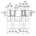
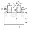
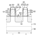
도 2는 도 1의 A - A를 따라서 절단한 단면도이다.
도 3은 도 2에서 제1 게이트 전극을 제외한 제1 게이트 스페이서를 도시한 도면이다.
도 4는 도 2에서, 제1 게이트 전극만을 분리하여 도시한 도면이다.
도 5는 도 2에서 제2 게이트 전극을 제외한 제2 게이트 스페이서를 도시한 도면이다.
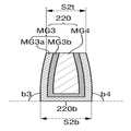
도 6은 도 2에서, 제2 게이트 전극만을 분리하여 도시한 도면이다.
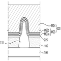
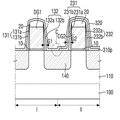
도 7a 내지 도 8b는 도 2의 B - B를 따라서 절단한 단면도이다.
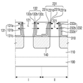
도 9a 내지 도 10b는 도 2의 C - C를 따라서 절단한 단면도이다.
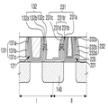
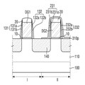
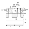
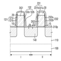
도 11은 본 발명의 몇몇 실시예에 따른 반도체 장치를 설명하기 위한 도면이다.
도 12는 본 발명의 몇몇 실시예에 따른 반도체 장치를 설명하기 위한 도면이다.
도 13은 본 발명의 몇몇 실시예에 따른 반도체 장치를 설명하기 위한 도면이다.
도 14 내지 19는 본 발명의 몇몇 실시예에 따른 반도체 장치 제조 방법을 설명하기 위한 중단 단계 도면들이다.
도 20은 본 발명의 몇몇 실시예에 따른 반도체 장치 제조 방법을 설명하기 위한 중간 단계의 도면이다.
도 21은 본 발명의 몇몇 실시예에 따른 반도체 장치 제조 방법을 설명하기 위한 중간 단계의 도면이다.
도 22 내지 도 26은 본 발명의 몇몇 실시예에 따른 반도체 장치 제조 방법을 설명하기 위한 중간 단계의 도면들이다.
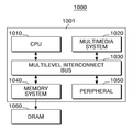
도 27은 본 발명의 실시예들에 따른 반도체 장치를 포함하는 SoC 시스템의 블록도이다.
110: 핀형 패턴 120, 220: 게이트 전극
180: 층간 절연막 131, 132, 231, 232: 게이트 스페이서
Claims (10)
- 기판 상에 형성되고, 하면의 폭에 대한 상면의 폭이 제1 비(ratio)를 가지는 제1 게이트 전극;
상기 기판 상에 형성되고, 하면의 폭에 대한 상면의 폭이 상기 제1 비보다 작은 제2 비를 가지는 제2 게이트 전극;
상기 제1 게이트 전극의 측벽 상에 형성되는 제1 게이트 스페이서;
상기 제2 게이트 전극의 측벽 상에 형성되는 제2 게이트 스페이서; 및
상기 제1 및 제2 게이트 스페이서를 덮는 층간 절연막을 포함하는 반도체 장치. - 제1 항에 있어서,
상기 제1 비는 1보다 크거나 같고,
상기 제2 비는 1보다 작거나 같은 반도체 장치. - 제1 항에 있어서,
상기 제1 및 제2 비는 1보다 크거나 같은 반도체 장치. - 제1 항에 있어서,
상기 제1 및 제2 비는 1보다 작거나 같은 반도체 장치. - 제1 항에 있어서,
상기 제1 게이트 전극은 N형이고,
상기 제2 게이트 전극은 P형인 반도체 장치. - 제5 항에 있어서,
상기 제1 게이트 전극은 N형 일함수 메탈을 포함하고,
상기 제2 게이트 전극은 N형 일함수 메탈 및 P형 일함수 메탈을 포함하는 반도체 장치. - 제1 항에 있어서,
상기 기판의 상면으로부터 멀어짐에 따라, 상기 제1 게이트 전극의 폭은 점차 좁아지는 반도체 장치. - 제7 항에 있어서,
상기 기판의 상면으로부터 멀어짐에 따라, 상기 제2 게이트 전극의 폭은 점차 넓어지는 반도체 장치. - 제1 항에 있어서,
상기 제1 게이트 스페이서는,
상기 제1 게이트 전극의 측벽 상에 형성되는 제1 질화 스페이서와,
상기 제1 질화 스페이서 상에 형성되는 제1 산화 스페이서와,
상기 제1 산화 스페이서 상에 형성되는 제1 스트레스 스페이서를 포함하는 반도체 장치. - 제9 항에 있어서,
상기 제2 게이트 스페이서는,
상기 제2 게이트 전극의 측벽 상에 형성되는 제2 질화 스페이서와,
상기 제2 질화 스페이서 상에 형성되는 제2 산화 스페이서와,
상기 제2 산화 스페이서 상에 형성되는 제2 스트레스 스페이서를 포함하는 반도체 장치.
Priority Applications (3)
| Application Number | Priority Date | Filing Date | Title |
|---|---|---|---|
| KR1020150148710A KR20170047953A (ko) | 2015-10-26 | 2015-10-26 | 반도체 장치 및 그 제조 방법 |
| US15/215,951 US20170117192A1 (en) | 2015-10-26 | 2016-07-21 | Semiconductor device and method of fabricating the same |
| CN201610916290.3A CN107039432A (zh) | 2015-10-26 | 2016-10-20 | 半导体器件 |
Applications Claiming Priority (1)
| Application Number | Priority Date | Filing Date | Title |
|---|---|---|---|
| KR1020150148710A KR20170047953A (ko) | 2015-10-26 | 2015-10-26 | 반도체 장치 및 그 제조 방법 |
Publications (1)
| Publication Number | Publication Date |
|---|---|
| KR20170047953A true KR20170047953A (ko) | 2017-05-08 |
Family
ID=58561869
Family Applications (1)
| Application Number | Title | Priority Date | Filing Date |
|---|---|---|---|
| KR1020150148710A Ceased KR20170047953A (ko) | 2015-10-26 | 2015-10-26 | 반도체 장치 및 그 제조 방법 |
Country Status (3)
| Country | Link |
|---|---|
| US (1) | US20170117192A1 (ko) |
| KR (1) | KR20170047953A (ko) |
| CN (1) | CN107039432A (ko) |
Cited By (2)
| Publication number | Priority date | Publication date | Assignee | Title |
|---|---|---|---|---|
| KR20190066583A (ko) * | 2017-12-05 | 2019-06-13 | 에이에스엠 아이피 홀딩 비.브이. | 스페이서-한정 패터닝을 위한 수직형 스페이서를 형성하는 방법 |
| KR20210002329A (ko) * | 2019-06-28 | 2021-01-07 | 타이완 세미콘덕터 매뉴팩쳐링 컴퍼니 리미티드 | 반도체 디바이스 및 제조 방법 |
Families Citing this family (15)
| Publication number | Priority date | Publication date | Assignee | Title |
|---|---|---|---|---|
| US9153668B2 (en) | 2013-05-23 | 2015-10-06 | Taiwan Semiconductor Manufacturing Company, Ltd. | Tuning tensile strain on FinFET |
| US10164049B2 (en) * | 2014-10-06 | 2018-12-25 | Taiwan Semiconductor Manufacturing Company, Ltd. | Structure and formation method of semiconductor device with gate stack |
| US9601567B1 (en) | 2015-10-30 | 2017-03-21 | Taiwan Semiconductor Manufacturing Co., Ltd. | Multiple Fin FET structures having an insulating separation plug |
| US9985031B2 (en) * | 2016-01-21 | 2018-05-29 | Taiwan Semiconductor Manufacturing Co., Ltd. | Integrated circuit and manufacturing method thereof |
| US9953883B2 (en) * | 2016-04-11 | 2018-04-24 | Samsung Electronics Co., Ltd. | Semiconductor device including a field effect transistor and method for manufacturing the same |
| US10147649B2 (en) * | 2016-05-27 | 2018-12-04 | Taiwan Semiconductor Manufacturing Co., Ltd. | Semiconductor device structure with gate stack and method for forming the same |
| US10153353B1 (en) | 2017-06-05 | 2018-12-11 | United Microelectronics Corp. | Semiconductor structure |
| KR102303300B1 (ko) * | 2017-08-04 | 2021-09-16 | 삼성전자주식회사 | 반도체 장치 |
| CN109585293B (zh) * | 2017-09-29 | 2021-12-24 | 台湾积体电路制造股份有限公司 | 切割金属工艺中的基脚去除 |
| US10903336B2 (en) * | 2017-11-28 | 2021-01-26 | Taiwan Semiconductor Manufacturing Co., Ltd. | Semiconductor device and method of manufacturing the same |
| US10879393B2 (en) * | 2018-08-14 | 2020-12-29 | Taiwan Semiconductor Manufacturing Co., Ltd. | Methods of fabricating semiconductor devices having gate structure with bent sidewalls |
| DE102020108047B4 (de) | 2019-10-31 | 2024-06-13 | Taiwan Semiconductor Manufacturing Co., Ltd. | Finnen-feldeffekttransistor-bauelement und verfahren zum bilden desselben |
| US11309403B2 (en) | 2019-10-31 | 2022-04-19 | Taiwan Semiconductor Manufacturing Company, Ltd. | Fin field-effect transistor device and method of forming the same |
| CN112420822B (zh) * | 2020-11-18 | 2024-06-07 | 上海华力集成电路制造有限公司 | 金属栅半导体器件及其制造方法 |
| US11824103B2 (en) * | 2021-04-23 | 2023-11-21 | Taiwan Semiconductor Manufacturing Company, Ltd. | Method of manufacturing a semiconductor device and a semiconductor device |
Family Cites Families (13)
| Publication number | Priority date | Publication date | Assignee | Title |
|---|---|---|---|---|
| US4757026A (en) * | 1986-11-04 | 1988-07-12 | Intel Corporation | Source drain doping technique |
| US7615418B2 (en) * | 2006-04-28 | 2009-11-10 | International Business Machines Corporation | High performance stress-enhance MOSFET and method of manufacture |
| KR100772901B1 (ko) * | 2006-09-28 | 2007-11-05 | 삼성전자주식회사 | 반도체 소자 및 이의 제조 방법 |
| US8338245B2 (en) * | 2006-12-14 | 2012-12-25 | Globalfoundries Singapore Pte. Ltd. | Integrated circuit system employing stress-engineered spacers |
| DE102007004824A1 (de) * | 2007-01-31 | 2008-08-07 | Advanced Micro Devices, Inc., Sunnyvale | Verbesserte Verspannungsübertragung in einem Zwischenschichtdielektrikum durch Verwendung einer zusätzlichen Verspannungsschicht über einer Schicht mit dualer Verspannung in einem Halbleiterbauelement |
| JP5130834B2 (ja) * | 2007-09-05 | 2013-01-30 | ソニー株式会社 | 半導体装置およびその製造方法 |
| US7883953B2 (en) * | 2008-09-30 | 2011-02-08 | Freescale Semiconductor, Inc. | Method for transistor fabrication with optimized performance |
| JP5531812B2 (ja) * | 2010-06-23 | 2014-06-25 | 富士通セミコンダクター株式会社 | Mosトランジスタおよびその製造方法、半導体集積回路装置 |
| US8629007B2 (en) * | 2011-07-14 | 2014-01-14 | International Business Machines Corporation | Method of improving replacement metal gate fill |
| CN103367363B (zh) * | 2012-03-27 | 2016-08-10 | 中国科学院微电子研究所 | 半导体器件及其制造方法 |
| KR20140121634A (ko) * | 2013-04-08 | 2014-10-16 | 삼성전자주식회사 | 반도체 장치 및 그 제조 방법 |
| US9252271B2 (en) * | 2013-11-27 | 2016-02-02 | Taiwan Semiconductor Manufacturing Company Limited | Semiconductor device and method of making |
| US9704759B2 (en) * | 2015-09-04 | 2017-07-11 | Globalfoundries Inc. | Methods of forming CMOS based integrated circuit products using disposable spacers |
-
2015
- 2015-10-26 KR KR1020150148710A patent/KR20170047953A/ko not_active Ceased
-
2016
- 2016-07-21 US US15/215,951 patent/US20170117192A1/en not_active Abandoned
- 2016-10-20 CN CN201610916290.3A patent/CN107039432A/zh active Pending
Cited By (2)
| Publication number | Priority date | Publication date | Assignee | Title |
|---|---|---|---|---|
| KR20190066583A (ko) * | 2017-12-05 | 2019-06-13 | 에이에스엠 아이피 홀딩 비.브이. | 스페이서-한정 패터닝을 위한 수직형 스페이서를 형성하는 방법 |
| KR20210002329A (ko) * | 2019-06-28 | 2021-01-07 | 타이완 세미콘덕터 매뉴팩쳐링 컴퍼니 리미티드 | 반도체 디바이스 및 제조 방법 |
Also Published As
| Publication number | Publication date |
|---|---|
| CN107039432A (zh) | 2017-08-11 |
| US20170117192A1 (en) | 2017-04-27 |
Similar Documents
| Publication | Publication Date | Title |
|---|---|---|
| KR20170047953A (ko) | 반도체 장치 및 그 제조 방법 | |
| KR102292812B1 (ko) | 반도체 장치 | |
| KR102422430B1 (ko) | 반도체 장치 및 그 제조 방법 | |
| US10580891B2 (en) | Semiconductor device and method for fabricating the same | |
| US11956937B2 (en) | Semiconductor device having fin-type pattern with varying widths along a center vertical line thereof | |
| KR20170090092A (ko) | 반도체 장치 및 이의 제조 방법 | |
| KR102270920B1 (ko) | 반도체 장치 및 이의 제조 방법 | |
| KR102426834B1 (ko) | 반도체 장치 | |
| US10692781B2 (en) | Semiconductor device | |
| KR102291062B1 (ko) | 반도체 장치 및 이의 제조 방법 | |
| KR20150111807A (ko) | 반도체 장치 및 이의 제조 방법 | |
| KR20170042064A (ko) | 반도체 장치 및 이의 제조 방법 | |
| KR20160066958A (ko) | 반도체 장치 | |
| KR20170000539A (ko) | 반도체 장치 | |
| KR20160118523A (ko) | 반도체 장치 | |
| US20240224487A1 (en) | Semiconductor Devices Including FINFET Structures with Increased Gate Surface | |
| KR20170021060A (ko) | 반도체 장치 | |
| KR102491538B1 (ko) | 반도체 장치 및 그 제조 방법 | |
| KR20170083822A (ko) | 반도체 장치 및 그 제조 방법 | |
| KR20170053094A (ko) | 반도체 장치 및 이의 제조 방법 | |
| KR20170000134A (ko) | 반도체 장치 및 이의 제조 방법 | |
| KR102360333B1 (ko) | 반도체 장치 | |
| KR20160132523A (ko) | 반도체 장치 | |
| KR102318131B1 (ko) | 반도체 장치 | |
| KR102419864B1 (ko) | 반도체 장치 |
Legal Events
| Date | Code | Title | Description |
|---|---|---|---|
| PA0109 | Patent application |
Patent event code: PA01091R01D Comment text: Patent Application Patent event date: 20151026 |
|
| PG1501 | Laying open of application | ||
| A201 | Request for examination | ||
| PA0201 | Request for examination |
Patent event code: PA02012R01D Patent event date: 20200910 Comment text: Request for Examination of Application Patent event code: PA02011R01I Patent event date: 20151026 Comment text: Patent Application |
|
| E902 | Notification of reason for refusal | ||
| PE0902 | Notice of grounds for rejection |
Comment text: Notification of reason for refusal Patent event date: 20211108 Patent event code: PE09021S01D |
|
| E601 | Decision to refuse application | ||
| PE0601 | Decision on rejection of patent |
Patent event date: 20220311 Comment text: Decision to Refuse Application Patent event code: PE06012S01D Patent event date: 20211108 Comment text: Notification of reason for refusal Patent event code: PE06011S01I |