KR20170061203A - 회로기판 및 제조방법 - Google Patents
회로기판 및 제조방법 Download PDFInfo
- Publication number
- KR20170061203A KR20170061203A KR1020150165178A KR20150165178A KR20170061203A KR 20170061203 A KR20170061203 A KR 20170061203A KR 1020150165178 A KR1020150165178 A KR 1020150165178A KR 20150165178 A KR20150165178 A KR 20150165178A KR 20170061203 A KR20170061203 A KR 20170061203A
- Authority
- KR
- South Korea
- Prior art keywords
- copper
- chip
- circuit board
- copper foil
- manufacturing
- Prior art date
- Legal status (The legal status is an assumption and is not a legal conclusion. Google has not performed a legal analysis and makes no representation as to the accuracy of the status listed.)
- Ceased
Links
- 238000004519 manufacturing process Methods 0.000 title claims abstract description 22
- RYGMFSIKBFXOCR-UHFFFAOYSA-N Copper Chemical compound [Cu] RYGMFSIKBFXOCR-UHFFFAOYSA-N 0.000 claims abstract description 70
- 239000011889 copper foil Substances 0.000 claims abstract description 20
- 238000000034 method Methods 0.000 claims abstract description 17
- 229910052802 copper Inorganic materials 0.000 claims abstract description 12
- 239000010949 copper Substances 0.000 claims abstract description 12
- 230000017525 heat dissipation Effects 0.000 claims abstract description 10
- 230000005855 radiation Effects 0.000 claims abstract description 10
- 239000000758 substrate Substances 0.000 claims abstract description 10
- 238000005530 etching Methods 0.000 claims abstract description 6
- 238000011161 development Methods 0.000 claims abstract description 5
- 239000002184 metal Substances 0.000 claims abstract description 4
- 229910052751 metal Inorganic materials 0.000 claims abstract description 4
- 238000007747 plating Methods 0.000 claims abstract description 4
- 239000000126 substance Substances 0.000 claims abstract description 4
- 238000004544 sputter deposition Methods 0.000 claims abstract description 3
- 239000011248 coating agent Substances 0.000 claims description 3
- 238000000576 coating method Methods 0.000 claims description 3
- 230000001678 irradiating effect Effects 0.000 claims description 2
- 238000012546 transfer Methods 0.000 abstract description 2
- 239000002390 adhesive tape Substances 0.000 description 7
- 238000007796 conventional method Methods 0.000 description 2
- 230000000191 radiation effect Effects 0.000 description 2
- 230000004075 alteration Effects 0.000 description 1
- 239000003054 catalyst Substances 0.000 description 1
- 238000005516 engineering process Methods 0.000 description 1
- 230000002708 enhancing effect Effects 0.000 description 1
- 210000003608 fece Anatomy 0.000 description 1
- 239000007888 film coating Substances 0.000 description 1
- 238000009501 film coating Methods 0.000 description 1
- 230000010354 integration Effects 0.000 description 1
- 238000003475 lamination Methods 0.000 description 1
- 239000000463 material Substances 0.000 description 1
- 238000012986 modification Methods 0.000 description 1
- 230000004048 modification Effects 0.000 description 1
- 238000002203 pretreatment Methods 0.000 description 1
- 238000006467 substitution reaction Methods 0.000 description 1
- 230000003746 surface roughness Effects 0.000 description 1
Images


Classifications
-
- H—ELECTRICITY
- H05—ELECTRIC TECHNIQUES NOT OTHERWISE PROVIDED FOR
- H05K—PRINTED CIRCUITS; CASINGS OR CONSTRUCTIONAL DETAILS OF ELECTRIC APPARATUS; MANUFACTURE OF ASSEMBLAGES OF ELECTRICAL COMPONENTS
- H05K3/00—Apparatus or processes for manufacturing printed circuits
- H05K3/10—Apparatus or processes for manufacturing printed circuits in which conductive material is applied to the insulating support in such a manner as to form the desired conductive pattern
- H05K3/20—Apparatus or processes for manufacturing printed circuits in which conductive material is applied to the insulating support in such a manner as to form the desired conductive pattern by affixing prefabricated conductor pattern
- H05K3/202—Apparatus or processes for manufacturing printed circuits in which conductive material is applied to the insulating support in such a manner as to form the desired conductive pattern by affixing prefabricated conductor pattern using self-supporting metal foil pattern
-
- H—ELECTRICITY
- H05—ELECTRIC TECHNIQUES NOT OTHERWISE PROVIDED FOR
- H05K—PRINTED CIRCUITS; CASINGS OR CONSTRUCTIONAL DETAILS OF ELECTRIC APPARATUS; MANUFACTURE OF ASSEMBLAGES OF ELECTRICAL COMPONENTS
- H05K3/00—Apparatus or processes for manufacturing printed circuits
- H05K3/02—Apparatus or processes for manufacturing printed circuits in which the conductive material is applied to the surface of the insulating support and is thereafter removed from such areas of the surface which are not intended for current conducting or shielding
- H05K3/06—Apparatus or processes for manufacturing printed circuits in which the conductive material is applied to the surface of the insulating support and is thereafter removed from such areas of the surface which are not intended for current conducting or shielding the conductive material being removed chemically or electrolytically, e.g. by photo-etch process
-
- H—ELECTRICITY
- H05—ELECTRIC TECHNIQUES NOT OTHERWISE PROVIDED FOR
- H05K—PRINTED CIRCUITS; CASINGS OR CONSTRUCTIONAL DETAILS OF ELECTRIC APPARATUS; MANUFACTURE OF ASSEMBLAGES OF ELECTRICAL COMPONENTS
- H05K3/00—Apparatus or processes for manufacturing printed circuits
- H05K3/22—Secondary treatment of printed circuits
- H05K3/28—Applying non-metallic protective coatings
-
- H—ELECTRICITY
- H05—ELECTRIC TECHNIQUES NOT OTHERWISE PROVIDED FOR
- H05K—PRINTED CIRCUITS; CASINGS OR CONSTRUCTIONAL DETAILS OF ELECTRIC APPARATUS; MANUFACTURE OF ASSEMBLAGES OF ELECTRICAL COMPONENTS
- H05K3/00—Apparatus or processes for manufacturing printed circuits
- H05K3/38—Improvement of the adhesion between the insulating substrate and the metal
- H05K3/382—Improvement of the adhesion between the insulating substrate and the metal by special treatment of the metal
-
- H—ELECTRICITY
- H05—ELECTRIC TECHNIQUES NOT OTHERWISE PROVIDED FOR
- H05K—PRINTED CIRCUITS; CASINGS OR CONSTRUCTIONAL DETAILS OF ELECTRIC APPARATUS; MANUFACTURE OF ASSEMBLAGES OF ELECTRICAL COMPONENTS
- H05K3/00—Apparatus or processes for manufacturing printed circuits
- H05K3/46—Manufacturing multilayer circuits
- H05K3/4697—Manufacturing multilayer circuits having cavities, e.g. for mounting components
Landscapes
- Engineering & Computer Science (AREA)
- Manufacturing & Machinery (AREA)
- Microelectronics & Electronic Packaging (AREA)
- Manufacturing Of Printed Wiring (AREA)
Abstract
Description
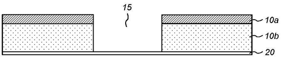
도2a 내지 도2d는 또 다른 종래기술에 따른 방열용 구리 칩을 제작하는 방법을 나타낸 도면.
도3a 내지 도3d는 본 발명에 따른 회로기판 제조방법을 나타낸 도면.
Claims (2)
- 방열용 구리 칩을 구비한 회로기판을 제조하는 방법에 있어서,
(a) 상기 제작하고자 하는 구리 칩의 두께 단차에 해당하는 두께를 지닌 동박을 절연층 위에 피복한 기판을 준비하는 단계;
(b) 상기 동박을 선택적으로 식각해서 절연층 위에 방열용 구리 칩을 형성하는 단계;
(c) 표면 전면을 조도 처리하여 표면 밀착력을 강화한 후 화학동 또는 스퍼터 방식으로 금속층을 형성하는 단계;
(d) 표면 전면에 상기 방열용 구리 칩 단차보다 두꺼운 두께의 드라이필름을 피복하고, 사진, 현상 등 일련의 이미지 프로세스를 진행해서 패턴을 전사한 후 동도금을 실시하는 단계; 및
(e) 상기 드라이필름을 박리 제거하고 플래시 에칭을 실시함으로써 상기 방열용 구리 칩과 동일층에 동박회로를 형성하는 단계
를 포함하는 회로기판 제조방법. - 방열용 구리 칩과 동일층에 동박회로를 구비한 회로기판으로서, 제1항의 제조방법에 따라 제작된 회로기판.
Priority Applications (1)
| Application Number | Priority Date | Filing Date | Title |
|---|---|---|---|
| KR1020150165178A KR20170061203A (ko) | 2015-11-25 | 2015-11-25 | 회로기판 및 제조방법 |
Applications Claiming Priority (1)
| Application Number | Priority Date | Filing Date | Title |
|---|---|---|---|
| KR1020150165178A KR20170061203A (ko) | 2015-11-25 | 2015-11-25 | 회로기판 및 제조방법 |
Publications (1)
| Publication Number | Publication Date |
|---|---|
| KR20170061203A true KR20170061203A (ko) | 2017-06-05 |
Family
ID=59222992
Family Applications (1)
| Application Number | Title | Priority Date | Filing Date |
|---|---|---|---|
| KR1020150165178A Ceased KR20170061203A (ko) | 2015-11-25 | 2015-11-25 | 회로기판 및 제조방법 |
Country Status (1)
| Country | Link |
|---|---|
| KR (1) | KR20170061203A (ko) |
Cited By (2)
| Publication number | Priority date | Publication date | Assignee | Title |
|---|---|---|---|---|
| CN116133238A (zh) * | 2023-03-20 | 2023-05-16 | 生益电子股份有限公司 | 一种pcb及其制作方法 |
| CN119255516A (zh) * | 2024-10-29 | 2025-01-03 | 江苏普诺威电子股份有限公司 | 阶梯厚铜嵌入式散热基板及其加工方法 |
-
2015
- 2015-11-25 KR KR1020150165178A patent/KR20170061203A/ko not_active Ceased
Cited By (2)
| Publication number | Priority date | Publication date | Assignee | Title |
|---|---|---|---|---|
| CN116133238A (zh) * | 2023-03-20 | 2023-05-16 | 生益电子股份有限公司 | 一种pcb及其制作方法 |
| CN119255516A (zh) * | 2024-10-29 | 2025-01-03 | 江苏普诺威电子股份有限公司 | 阶梯厚铜嵌入式散热基板及其加工方法 |
Similar Documents
| Publication | Publication Date | Title |
|---|---|---|
| JP6996976B2 (ja) | プリント回路基板のための高速インターコネクト | |
| US8435376B2 (en) | Carrier for manufacturing substrate and method of manufacturing substrate using the same | |
| JP2012124452A (ja) | プリント基板およびその製造方法 | |
| KR20110029469A (ko) | 인쇄회로기판 및 그의 제조 방법 | |
| US9497853B2 (en) | Printed circuit board and method for manufacturing the same | |
| JP2012227557A (ja) | プリント基板の製造方法 | |
| JP2013526774A (ja) | 両面フレキシブルプリント回路基板及びその製造方法 | |
| KR20170061203A (ko) | 회로기판 및 제조방법 | |
| US7992296B2 (en) | PCB and manufacturing method thereof | |
| KR101419200B1 (ko) | 플렉서블 인쇄회로기판의 제조방법 | |
| JP2019125631A (ja) | 配線部品、照明装置、電気電子機器、及び配線部品の製造方法 | |
| JP2007288022A (ja) | 多層プリント配線板及びその製造方法 | |
| US9288902B2 (en) | Printed circuit board and method of manufacturing the same | |
| CN106332444B (zh) | 电路板及其制作方法 | |
| CN103717015A (zh) | 柔性印刷电路板制造方法 | |
| KR20120002016A (ko) | 연성인쇄회로기판의 제조방법 | |
| KR101119380B1 (ko) | 기판 제조용 캐리어 부재 및 이를 이용한 기판의 제조방법 | |
| JP5287570B2 (ja) | プリント配線板の製造方法 | |
| KR101533013B1 (ko) | 플렉서블 인쇄회로기판의 제조방법 | |
| KR101436827B1 (ko) | 인쇄회로기판 및 제조방법 | |
| CN111128679A (zh) | 一种功分微波基板以及制作方法 | |
| KR20160029899A (ko) | 인쇄회로기판 및 제조방법 | |
| KR20140137628A (ko) | 연성회로기판의 구조 | |
| JPH11307888A (ja) | 放熱層埋め込み型回路基板の製造方法 | |
| KR20120036037A (ko) | 칩 내장형 인쇄회로기판 제조방법 |
Legal Events
| Date | Code | Title | Description |
|---|---|---|---|
| A201 | Request for examination | ||
| PA0109 | Patent application |
Patent event code: PA01091R01D Comment text: Patent Application Patent event date: 20151125 |
|
| PA0201 | Request for examination | ||
| E902 | Notification of reason for refusal | ||
| PE0902 | Notice of grounds for rejection |
Comment text: Notification of reason for refusal Patent event date: 20170201 Patent event code: PE09021S01D |
|
| PG1501 | Laying open of application | ||
| E601 | Decision to refuse application | ||
| PE0601 | Decision on rejection of patent |
Patent event date: 20170705 Comment text: Decision to Refuse Application Patent event code: PE06012S01D Patent event date: 20170201 Comment text: Notification of reason for refusal Patent event code: PE06011S01I |