KR20170121164A - 터치 패널용 도전성 적층체, 및 터치 패널용 도전성 적층체의 제조 방법 - Google Patents
터치 패널용 도전성 적층체, 및 터치 패널용 도전성 적층체의 제조 방법 Download PDFInfo
- Publication number
- KR20170121164A KR20170121164A KR1020177021911A KR20177021911A KR20170121164A KR 20170121164 A KR20170121164 A KR 20170121164A KR 1020177021911 A KR1020177021911 A KR 1020177021911A KR 20177021911 A KR20177021911 A KR 20177021911A KR 20170121164 A KR20170121164 A KR 20170121164A
- Authority
- KR
- South Korea
- Prior art keywords
- layer
- copper
- oxynitride layer
- touch panel
- oxynitride
- Prior art date
- Legal status (The legal status is an assumption and is not a legal conclusion. Google has not performed a legal analysis and makes no representation as to the accuracy of the status listed.)
- Granted
Links
Images



Classifications
-
- C—CHEMISTRY; METALLURGY
- C23—COATING METALLIC MATERIAL; COATING MATERIAL WITH METALLIC MATERIAL; CHEMICAL SURFACE TREATMENT; DIFFUSION TREATMENT OF METALLIC MATERIAL; COATING BY VACUUM EVAPORATION, BY SPUTTERING, BY ION IMPLANTATION OR BY CHEMICAL VAPOUR DEPOSITION, IN GENERAL; INHIBITING CORROSION OF METALLIC MATERIAL OR INCRUSTATION IN GENERAL
- C23C—COATING METALLIC MATERIAL; COATING MATERIAL WITH METALLIC MATERIAL; SURFACE TREATMENT OF METALLIC MATERIAL BY DIFFUSION INTO THE SURFACE, BY CHEMICAL CONVERSION OR SUBSTITUTION; COATING BY VACUUM EVAPORATION, BY SPUTTERING, BY ION IMPLANTATION OR BY CHEMICAL VAPOUR DEPOSITION, IN GENERAL
- C23C14/00—Coating by vacuum evaporation, by sputtering or by ion implantation of the coating forming material
- C23C14/06—Coating by vacuum evaporation, by sputtering or by ion implantation of the coating forming material characterised by the coating material
- C23C14/14—Metallic material, boron or silicon
-
- B—PERFORMING OPERATIONS; TRANSPORTING
- B32—LAYERED PRODUCTS
- B32B—LAYERED PRODUCTS, i.e. PRODUCTS BUILT-UP OF STRATA OF FLAT OR NON-FLAT, e.g. CELLULAR OR HONEYCOMB, FORM
- B32B9/00—Layered products comprising a layer of a particular substance not covered by groups B32B11/00 - B32B29/00
- B32B9/04—Layered products comprising a layer of a particular substance not covered by groups B32B11/00 - B32B29/00 comprising such particular substance as the main or only constituent of a layer, which is next to another layer of the same or of a different material
- B32B9/041—Layered products comprising a layer of a particular substance not covered by groups B32B11/00 - B32B29/00 comprising such particular substance as the main or only constituent of a layer, which is next to another layer of the same or of a different material of metal
-
- B—PERFORMING OPERATIONS; TRANSPORTING
- B32—LAYERED PRODUCTS
- B32B—LAYERED PRODUCTS, i.e. PRODUCTS BUILT-UP OF STRATA OF FLAT OR NON-FLAT, e.g. CELLULAR OR HONEYCOMB, FORM
- B32B15/00—Layered products comprising a layer of metal
- B32B15/04—Layered products comprising a layer of metal comprising metal as the main or only constituent of a layer, which is next to another layer of the same or of a different material
- B32B15/08—Layered products comprising a layer of metal comprising metal as the main or only constituent of a layer, which is next to another layer of the same or of a different material of synthetic resin
-
- B—PERFORMING OPERATIONS; TRANSPORTING
- B32—LAYERED PRODUCTS
- B32B—LAYERED PRODUCTS, i.e. PRODUCTS BUILT-UP OF STRATA OF FLAT OR NON-FLAT, e.g. CELLULAR OR HONEYCOMB, FORM
- B32B15/00—Layered products comprising a layer of metal
- B32B15/04—Layered products comprising a layer of metal comprising metal as the main or only constituent of a layer, which is next to another layer of the same or of a different material
- B32B15/08—Layered products comprising a layer of metal comprising metal as the main or only constituent of a layer, which is next to another layer of the same or of a different material of synthetic resin
- B32B15/082—Layered products comprising a layer of metal comprising metal as the main or only constituent of a layer, which is next to another layer of the same or of a different material of synthetic resin comprising vinyl resins; comprising acrylic resins
-
- B—PERFORMING OPERATIONS; TRANSPORTING
- B32—LAYERED PRODUCTS
- B32B—LAYERED PRODUCTS, i.e. PRODUCTS BUILT-UP OF STRATA OF FLAT OR NON-FLAT, e.g. CELLULAR OR HONEYCOMB, FORM
- B32B15/00—Layered products comprising a layer of metal
- B32B15/20—Layered products comprising a layer of metal comprising aluminium or copper
-
- B—PERFORMING OPERATIONS; TRANSPORTING
- B32—LAYERED PRODUCTS
- B32B—LAYERED PRODUCTS, i.e. PRODUCTS BUILT-UP OF STRATA OF FLAT OR NON-FLAT, e.g. CELLULAR OR HONEYCOMB, FORM
- B32B27/00—Layered products comprising a layer of synthetic resin
- B32B27/18—Layered products comprising a layer of synthetic resin characterised by the use of special additives
-
- B—PERFORMING OPERATIONS; TRANSPORTING
- B32—LAYERED PRODUCTS
- B32B—LAYERED PRODUCTS, i.e. PRODUCTS BUILT-UP OF STRATA OF FLAT OR NON-FLAT, e.g. CELLULAR OR HONEYCOMB, FORM
- B32B27/00—Layered products comprising a layer of synthetic resin
- B32B27/30—Layered products comprising a layer of synthetic resin comprising vinyl (co)polymers; comprising acrylic (co)polymers
- B32B27/308—Layered products comprising a layer of synthetic resin comprising vinyl (co)polymers; comprising acrylic (co)polymers comprising acrylic (co)polymers
-
- B—PERFORMING OPERATIONS; TRANSPORTING
- B32—LAYERED PRODUCTS
- B32B—LAYERED PRODUCTS, i.e. PRODUCTS BUILT-UP OF STRATA OF FLAT OR NON-FLAT, e.g. CELLULAR OR HONEYCOMB, FORM
- B32B9/00—Layered products comprising a layer of a particular substance not covered by groups B32B11/00 - B32B29/00
-
- B—PERFORMING OPERATIONS; TRANSPORTING
- B32—LAYERED PRODUCTS
- B32B—LAYERED PRODUCTS, i.e. PRODUCTS BUILT-UP OF STRATA OF FLAT OR NON-FLAT, e.g. CELLULAR OR HONEYCOMB, FORM
- B32B9/00—Layered products comprising a layer of a particular substance not covered by groups B32B11/00 - B32B29/00
- B32B9/04—Layered products comprising a layer of a particular substance not covered by groups B32B11/00 - B32B29/00 comprising such particular substance as the main or only constituent of a layer, which is next to another layer of the same or of a different material
- B32B9/045—Layered products comprising a layer of a particular substance not covered by groups B32B11/00 - B32B29/00 comprising such particular substance as the main or only constituent of a layer, which is next to another layer of the same or of a different material of synthetic resin
-
- C—CHEMISTRY; METALLURGY
- C23—COATING METALLIC MATERIAL; COATING MATERIAL WITH METALLIC MATERIAL; CHEMICAL SURFACE TREATMENT; DIFFUSION TREATMENT OF METALLIC MATERIAL; COATING BY VACUUM EVAPORATION, BY SPUTTERING, BY ION IMPLANTATION OR BY CHEMICAL VAPOUR DEPOSITION, IN GENERAL; INHIBITING CORROSION OF METALLIC MATERIAL OR INCRUSTATION IN GENERAL
- C23C—COATING METALLIC MATERIAL; COATING MATERIAL WITH METALLIC MATERIAL; SURFACE TREATMENT OF METALLIC MATERIAL BY DIFFUSION INTO THE SURFACE, BY CHEMICAL CONVERSION OR SUBSTITUTION; COATING BY VACUUM EVAPORATION, BY SPUTTERING, BY ION IMPLANTATION OR BY CHEMICAL VAPOUR DEPOSITION, IN GENERAL
- C23C14/00—Coating by vacuum evaporation, by sputtering or by ion implantation of the coating forming material
- C23C14/0021—Reactive sputtering or evaporation
- C23C14/0036—Reactive sputtering
-
- C—CHEMISTRY; METALLURGY
- C23—COATING METALLIC MATERIAL; COATING MATERIAL WITH METALLIC MATERIAL; CHEMICAL SURFACE TREATMENT; DIFFUSION TREATMENT OF METALLIC MATERIAL; COATING BY VACUUM EVAPORATION, BY SPUTTERING, BY ION IMPLANTATION OR BY CHEMICAL VAPOUR DEPOSITION, IN GENERAL; INHIBITING CORROSION OF METALLIC MATERIAL OR INCRUSTATION IN GENERAL
- C23C—COATING METALLIC MATERIAL; COATING MATERIAL WITH METALLIC MATERIAL; SURFACE TREATMENT OF METALLIC MATERIAL BY DIFFUSION INTO THE SURFACE, BY CHEMICAL CONVERSION OR SUBSTITUTION; COATING BY VACUUM EVAPORATION, BY SPUTTERING, BY ION IMPLANTATION OR BY CHEMICAL VAPOUR DEPOSITION, IN GENERAL
- C23C14/00—Coating by vacuum evaporation, by sputtering or by ion implantation of the coating forming material
- C23C14/02—Pretreatment of the material to be coated
- C23C14/024—Deposition of sublayers, e.g. to promote adhesion of the coating
-
- C—CHEMISTRY; METALLURGY
- C23—COATING METALLIC MATERIAL; COATING MATERIAL WITH METALLIC MATERIAL; CHEMICAL SURFACE TREATMENT; DIFFUSION TREATMENT OF METALLIC MATERIAL; COATING BY VACUUM EVAPORATION, BY SPUTTERING, BY ION IMPLANTATION OR BY CHEMICAL VAPOUR DEPOSITION, IN GENERAL; INHIBITING CORROSION OF METALLIC MATERIAL OR INCRUSTATION IN GENERAL
- C23C—COATING METALLIC MATERIAL; COATING MATERIAL WITH METALLIC MATERIAL; SURFACE TREATMENT OF METALLIC MATERIAL BY DIFFUSION INTO THE SURFACE, BY CHEMICAL CONVERSION OR SUBSTITUTION; COATING BY VACUUM EVAPORATION, BY SPUTTERING, BY ION IMPLANTATION OR BY CHEMICAL VAPOUR DEPOSITION, IN GENERAL
- C23C14/00—Coating by vacuum evaporation, by sputtering or by ion implantation of the coating forming material
- C23C14/06—Coating by vacuum evaporation, by sputtering or by ion implantation of the coating forming material characterised by the coating material
-
- C—CHEMISTRY; METALLURGY
- C23—COATING METALLIC MATERIAL; COATING MATERIAL WITH METALLIC MATERIAL; CHEMICAL SURFACE TREATMENT; DIFFUSION TREATMENT OF METALLIC MATERIAL; COATING BY VACUUM EVAPORATION, BY SPUTTERING, BY ION IMPLANTATION OR BY CHEMICAL VAPOUR DEPOSITION, IN GENERAL; INHIBITING CORROSION OF METALLIC MATERIAL OR INCRUSTATION IN GENERAL
- C23C—COATING METALLIC MATERIAL; COATING MATERIAL WITH METALLIC MATERIAL; SURFACE TREATMENT OF METALLIC MATERIAL BY DIFFUSION INTO THE SURFACE, BY CHEMICAL CONVERSION OR SUBSTITUTION; COATING BY VACUUM EVAPORATION, BY SPUTTERING, BY ION IMPLANTATION OR BY CHEMICAL VAPOUR DEPOSITION, IN GENERAL
- C23C14/00—Coating by vacuum evaporation, by sputtering or by ion implantation of the coating forming material
- C23C14/06—Coating by vacuum evaporation, by sputtering or by ion implantation of the coating forming material characterised by the coating material
- C23C14/0676—Oxynitrides
-
- G—PHYSICS
- G06—COMPUTING OR CALCULATING; COUNTING
- G06F—ELECTRIC DIGITAL DATA PROCESSING
- G06F3/00—Input arrangements for transferring data to be processed into a form capable of being handled by the computer; Output arrangements for transferring data from processing unit to output unit, e.g. interface arrangements
- G06F3/01—Input arrangements or combined input and output arrangements for interaction between user and computer
- G06F3/03—Arrangements for converting the position or the displacement of a member into a coded form
- G06F3/041—Digitisers, e.g. for touch screens or touch pads, characterised by the transducing means
-
- B—PERFORMING OPERATIONS; TRANSPORTING
- B32—LAYERED PRODUCTS
- B32B—LAYERED PRODUCTS, i.e. PRODUCTS BUILT-UP OF STRATA OF FLAT OR NON-FLAT, e.g. CELLULAR OR HONEYCOMB, FORM
- B32B2307/00—Properties of the layers or laminate
- B32B2307/20—Properties of the layers or laminate having particular electrical or magnetic properties, e.g. piezoelectric
- B32B2307/202—Conductive
-
- B—PERFORMING OPERATIONS; TRANSPORTING
- B32—LAYERED PRODUCTS
- B32B—LAYERED PRODUCTS, i.e. PRODUCTS BUILT-UP OF STRATA OF FLAT OR NON-FLAT, e.g. CELLULAR OR HONEYCOMB, FORM
- B32B2457/00—Electrical equipment
- B32B2457/20—Displays, e.g. liquid crystal displays, plasma displays
- B32B2457/208—Touch screens
-
- G—PHYSICS
- G06—COMPUTING OR CALCULATING; COUNTING
- G06F—ELECTRIC DIGITAL DATA PROCESSING
- G06F2203/00—Indexing scheme relating to G06F3/00 - G06F3/048
- G06F2203/041—Indexing scheme relating to G06F3/041 - G06F3/045
- G06F2203/04103—Manufacturing, i.e. details related to manufacturing processes specially suited for touch sensitive devices
Landscapes
- Chemical & Material Sciences (AREA)
- Engineering & Computer Science (AREA)
- Mechanical Engineering (AREA)
- Organic Chemistry (AREA)
- Metallurgy (AREA)
- Chemical Kinetics & Catalysis (AREA)
- Materials Engineering (AREA)
- General Engineering & Computer Science (AREA)
- Theoretical Computer Science (AREA)
- General Physics & Mathematics (AREA)
- Physics & Mathematics (AREA)
- Human Computer Interaction (AREA)
- Ceramic Engineering (AREA)
- Laminated Bodies (AREA)
- Non-Insulated Conductors (AREA)
- Manufacturing Of Electric Cables (AREA)
- Position Input By Displaying (AREA)
Abstract
Description
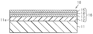
도 2 는, 터치 패널용 도전성 적층체의 일례에 있어서의 단면 구조를 모식적으로 나타내는 단면도이다.
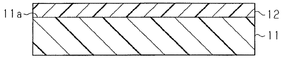
도 3 은, 터치 패널용 도전성 적층체의 제조 방법 중, 하지층을 형성하는 공정을 설명하기 위한 공정도이다.
도 4 는, 기재와 하지층의 일부를 확대하여 나타내는 부분 확대 단면도이다.
도 5 는, 터치 패널용 도전성 적층체의 제조 방법 중, 하측 산질화구리층을 형성하는 공정을 설명하기 위한 공정도이다.
도 6 은, 터치 패널용 도전성 적층체의 제조 방법 중, 구리층을 형성하는 공정을 설명하기 위한 공정도이다.
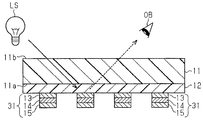
도 7 은, 터치 패널용 도전성 적층체의 작용을 설명하기 위한 작용도이다.
도 8 은, 터치 패널용 도전성 적층체의 작용을 설명하기 위한 작용도이다.



11 : 기재
11a : 제 1 면
11b : 제 2 면
11c : 오목부
12, 21 : 하지층
13, 22 : 하측 산질화구리층
14, 23 : 구리층
15, 24 : 상측 산질화구리층
16 : 제 1 적층체
20 : 제 2 적층체
31 : 전극
Claims (10)
- 하나의 면을 구비함과 함께, 광 투과성을 갖는 기재와,
상기 기재의 상기 하나의 면에 위치함과 함께, 광 투과성을 갖는 하지층과,
상기 하지층 중, 상기 기재에 접하는 면과는 반대측의 면에 위치하는 제 1 산질화구리층과,
상기 제 1 산질화구리층 중, 상기 하지층에 접하는 면과는 반대측의 면에 위치하는 구리층과,
상기 구리층 중, 상기 제 1 산질화구리층에 접하는 면과는 반대측의 면에 위치하는 제 2 산질화구리층을 구비하는, 터치 패널용 도전성 적층체. - 제 1 면과, 상기 제 1 면과는 반대측의 제 2 면을 구비하는 기재와,
상기 제 1 면, 및 상기 제 2 면에 각각 위치함과 함께, 광 투과성을 갖는 하지층과,
상기 하지층 중, 상기 기재에 접하는 면과는 반대측의 면에 위치하는 제 1 산질화구리층과,
상기 제 1 산질화구리층 중, 상기 하지층에 접하는 면과는 반대측의 면에 위치하는 구리층과,
상기 구리층 중, 상기 제 1 산질화구리층에 접하는 면과는 반대측의 면에 위치하는 제 2 산질화구리층을 구비하는, 터치 패널용 도전성 적층체. - 제 1 항 또는 제 2 항에 있어서,
상기 하지층은, 자외선 경화성 다관능 아크릴레이트, 자외선 경화성 단관능 아크릴레이트, 자외선 경화성의 아크릴기를 포함하는 아크릴 폴리머, 및 상기 제 2 산질화구리층 중 상기 구리층과는 반대측의 면에 있어서의 밀착성을 낮추기 위한 안티블로킹제를 포함하고,
상기 하지층은, 상기 기재에 있어서 상기 하지층이 접하는 면에 형성된 복수의 오목부를 메우는, 터치 패널용 도전성 적층체. - 제 1 항 내지 제 3 항 중 어느 한 항에 있어서,
상기 구리층의 두께는 200 ㎚ 이상 500 ㎚ 이하이고,
상기 제 1 산질화구리층의 두께는 30 ㎚ 이상 50 ㎚ 이하이고, 또한, 상기 구리층의 두께에 있어서의 25 % 이하의 값인, 터치 패널용 도전성 적층체. - 제 1 항 내지 제 4 항 중 어느 한 항에 있어서,
상기 제 2 산질화구리층에 있어서, XYZ 표색계에 있어서의 3 자극값 중 Y 의 값으로서, 상기 제 2 산질화구리층이 형성된 시점에서의 상기 Y 의 값이 20 % 이하인, 터치 패널용 도전성 적층체. - 제 1 항 내지 제 5 항 중 어느 한 항에 있어서,
상기 제 1 산질화구리층 및 상기 제 2 산질화구리층의 적어도 일방은, 4 원자% 이상 19 원자% 이하의 비율로 산소 원자를 포함하는, 터치 패널용 도전성 적층체. - 제 1 항 내지 제 6 항 중 어느 한 항에 있어서,
상기 하지층과 상기 제 1 산질화구리층의 계면에 있어서의 밀착 강도가 8.0 N/15 ㎜ 이상인, 터치 패널용 도전성 적층체. - 제 4 항에 있어서,
상기 제 1 산질화구리층, 상기 구리층, 및 상기 제 2 산질화구리층으로 구성되는 적층체에 있어서의 표면 저항률이 0.13 Ω/□ 이하인, 터치 패널용 도전성 적층체. - 제 1 항 내지 제 8 항 중 어느 한 항에 있어서,
상기 하지층 중, 상기 제 1 산질화구리층에 접하는 면에 있어서의 표면 조도 Ra 가 3 ㎚ 이상 20 ㎚ 이하인, 터치 패널용 도전성 적층체. - 기재에 있어서의 적어도 하나의 면에 하지층을 형성하는 공정과,
상기 하지층 중, 상기 기재에 접하는 면과는 반대측의 면에, 스퍼터법을 사용하여 제 1 산질화구리층을 형성하는 공정과,
상기 제 1 산질화구리층 중, 상기 하지층에 접하는 면과는 반대측의 면에, 스퍼터법을 사용하여 구리층을 형성하는 공정과,
상기 구리층 중, 상기 제 1 산질화구리층에 접하는 면과는 반대측의 면에, 스퍼터법을 사용하여 제 2 산질화구리층을 형성하는 공정을 구비하는, 터치 패널용 도전성 적층체의 제조 방법.
Applications Claiming Priority (3)
| Application Number | Priority Date | Filing Date | Title |
|---|---|---|---|
| JP2015035707 | 2015-02-25 | ||
| JPJP-P-2015-035707 | 2015-02-25 | ||
| PCT/JP2015/086361 WO2016136117A1 (ja) | 2015-02-25 | 2015-12-25 | タッチパネル用導電性積層体、および、タッチパネル用導電性積層体の製造方法 |
Publications (2)
| Publication Number | Publication Date |
|---|---|
| KR20170121164A true KR20170121164A (ko) | 2017-11-01 |
| KR102475311B1 KR102475311B1 (ko) | 2022-12-06 |
Family
ID=56788148
Family Applications (1)
| Application Number | Title | Priority Date | Filing Date |
|---|---|---|---|
| KR1020177021911A Active KR102475311B1 (ko) | 2015-02-25 | 2015-12-25 | 터치 패널용 도전성 적층체, 및 터치 패널용 도전성 적층체의 제조 방법 |
Country Status (9)
| Country | Link |
|---|---|
| US (1) | US10526693B2 (ko) |
| EP (1) | EP3264233B1 (ko) |
| JP (1) | JP6607918B2 (ko) |
| KR (1) | KR102475311B1 (ko) |
| CN (1) | CN107209600B (ko) |
| ES (1) | ES2724023T3 (ko) |
| PT (1) | PT3264233T (ko) |
| TW (1) | TWI697817B (ko) |
| WO (1) | WO2016136117A1 (ko) |
Families Citing this family (9)
| Publication number | Priority date | Publication date | Assignee | Title |
|---|---|---|---|---|
| US10527938B2 (en) * | 2014-11-05 | 2020-01-07 | Nissha Co., Ltd. | Method for producing electrical wiring member and electrical wiring member |
| CN109563625B (zh) * | 2016-08-08 | 2021-06-22 | Dic株式会社 | 层叠体、金属网和触控面板 |
| JP6939477B2 (ja) * | 2017-11-29 | 2021-09-22 | 大同特殊鋼株式会社 | 積層体 |
| KR102201575B1 (ko) * | 2017-12-15 | 2021-01-12 | 주식회사 엘지화학 | 장식 부재 |
| US11971564B2 (en) | 2017-12-15 | 2024-04-30 | Lg Chem, Ltd. | Decorative member and manufacturing method therefor |
| CN108511491B (zh) * | 2018-03-30 | 2021-04-02 | 京东方科技集团股份有限公司 | 显示基板和显示面板及其制作方法、驱动方法、显示装置 |
| JP7395244B2 (ja) * | 2018-06-12 | 2023-12-11 | 日東電工株式会社 | ハードコートフィルムおよび透明導電性フィルム |
| TWI773921B (zh) * | 2019-08-30 | 2022-08-11 | 洋華光電股份有限公司 | 在觸控感應器的透明電極上形成輔助導電單元的製造方法及其製成品 |
| KR102766203B1 (ko) * | 2020-02-04 | 2025-02-13 | 미쓰이금속광업주식회사 | 캐리어 구비 금속박 |
Citations (3)
| Publication number | Priority date | Publication date | Assignee | Title |
|---|---|---|---|---|
| JP2011028699A (ja) | 2009-07-21 | 2011-02-10 | Touch Panel Kenkyusho:Kk | 静電容量式タッチパネル構造体 |
| JP2013540331A (ja) * | 2010-10-19 | 2013-10-31 | エルジー・ケム・リミテッド | 導電性パターンを含むタッチパネルおよびその製造方法 |
| JP2015005272A (ja) * | 2013-05-22 | 2015-01-08 | 日東電工株式会社 | 両面透明導電性フィルムおよびタッチパネル |
Family Cites Families (10)
| Publication number | Priority date | Publication date | Assignee | Title |
|---|---|---|---|---|
| WO2012134174A2 (ko) * | 2011-03-28 | 2012-10-04 | 주식회사 엘지화학 | 전도성 구조체, 터치패널 및 이의 제조방법 |
| JP5473990B2 (ja) * | 2011-06-17 | 2014-04-16 | 日東電工株式会社 | 導電性積層体、パターン配線付き透明導電性積層体、および光学デバイス。 |
| JP6099875B2 (ja) * | 2011-11-22 | 2017-03-22 | 東レ株式会社 | 積層体の製造方法 |
| JP6004874B2 (ja) * | 2011-12-16 | 2016-10-12 | 日東電工株式会社 | 透明導電性フィルム |
| WO2013172055A1 (ja) * | 2012-05-17 | 2013-11-21 | 株式会社カネカ | 透明電極付き基板およびその製造方法、ならびにタッチパネル |
| CN104603886B (zh) * | 2012-08-31 | 2016-12-07 | Lg化学株式会社 | 导电结构及其制造方法 |
| TW201443757A (zh) * | 2013-05-13 | 2014-11-16 | Wintek Corp | 觸控面板 |
| JP6129769B2 (ja) * | 2013-05-24 | 2017-05-17 | 富士フイルム株式会社 | タッチパネル用透明導電膜、透明導電膜の製造方法、タッチパネル及び表示装置 |
| TW201504875A (zh) * | 2013-07-23 | 2015-02-01 | Wintek Corp | 觸控面板 |
| TWI545595B (zh) * | 2013-11-20 | 2016-08-11 | Lg化學股份有限公司 | 導電結構體及其製造方法 |
-
2015
- 2015-12-25 WO PCT/JP2015/086361 patent/WO2016136117A1/ja not_active Ceased
- 2015-12-25 PT PT15883407T patent/PT3264233T/pt unknown
- 2015-12-25 ES ES15883407T patent/ES2724023T3/es active Active
- 2015-12-25 KR KR1020177021911A patent/KR102475311B1/ko active Active
- 2015-12-25 CN CN201580076230.9A patent/CN107209600B/zh active Active
- 2015-12-25 EP EP15883407.7A patent/EP3264233B1/en active Active
- 2015-12-25 JP JP2017501882A patent/JP6607918B2/ja active Active
-
2016
- 2016-06-03 TW TW105117495A patent/TWI697817B/zh active
-
2017
- 2017-08-25 US US15/686,238 patent/US10526693B2/en active Active
Patent Citations (3)
| Publication number | Priority date | Publication date | Assignee | Title |
|---|---|---|---|---|
| JP2011028699A (ja) | 2009-07-21 | 2011-02-10 | Touch Panel Kenkyusho:Kk | 静電容量式タッチパネル構造体 |
| JP2013540331A (ja) * | 2010-10-19 | 2013-10-31 | エルジー・ケム・リミテッド | 導電性パターンを含むタッチパネルおよびその製造方法 |
| JP2015005272A (ja) * | 2013-05-22 | 2015-01-08 | 日東電工株式会社 | 両面透明導電性フィルムおよびタッチパネル |
Also Published As
| Publication number | Publication date |
|---|---|
| JP6607918B2 (ja) | 2019-11-20 |
| PT3264233T (pt) | 2019-05-24 |
| WO2016136117A1 (ja) | 2016-09-01 |
| TW201730727A (zh) | 2017-09-01 |
| JPWO2016136117A1 (ja) | 2017-12-28 |
| US20170349998A1 (en) | 2017-12-07 |
| US10526693B2 (en) | 2020-01-07 |
| EP3264233A1 (en) | 2018-01-03 |
| EP3264233A4 (en) | 2018-07-11 |
| CN107209600B (zh) | 2021-03-26 |
| ES2724023T3 (es) | 2019-09-05 |
| KR102475311B1 (ko) | 2022-12-06 |
| EP3264233B1 (en) | 2019-02-27 |
| CN107209600A (zh) | 2017-09-26 |
| TWI697817B (zh) | 2020-07-01 |
Similar Documents
| Publication | Publication Date | Title |
|---|---|---|
| KR20170121164A (ko) | 터치 패널용 도전성 적층체, 및 터치 패널용 도전성 적층체의 제조 방법 | |
| EP1947551B1 (en) | Transparent conductive film , method for production thereof and touch panel therewith | |
| KR100563419B1 (ko) | 광 흡수성 반사방지체 및 그 제조 방법 | |
| CN103443748B (zh) | 带有透明电极的基板及其制造方法以及触摸面板 | |
| KR20120047828A (ko) | 투명 도전성 필름 및 터치 패널 | |
| WO2011040403A1 (ja) | 透明導電性フィルム及びタッチパネル | |
| JP5190854B2 (ja) | 透明導電フィルム及び透明導電積層体並びにタッチパネル | |
| KR102558619B1 (ko) | 투명 도전성 필름 | |
| KR20160043154A (ko) | 적층체, 그의 제조방법 및 전자기기 | |
| KR20140116002A (ko) | 전자 부품용 적층 배선막 및 피복층 형성용 스퍼터링 타깃재 | |
| WO2014020656A1 (ja) | 透明導電フィルム及びタッチパネル | |
| JP5425423B2 (ja) | 透明導電性フィルム及びタッチパネル、並びに透明導電性フィルムの製造方法 | |
| KR20250065014A (ko) | 다층 금속 박막 구조체 및 그 제조방법 | |
| CN111145938A (zh) | 导电性薄膜及触摸面板 | |
| JP6413663B2 (ja) | 金属積層フィルム | |
| US20210333438A1 (en) | Multilayer antireflective article and methods of forming the same | |
| KR20160127295A (ko) | 전도성 암색화층을 구비한 전도성 구조체, 및 그 제조 장치 및 제조 방법 |
Legal Events
| Date | Code | Title | Description |
|---|---|---|---|
| PA0105 | International application |
St.27 status event code: A-0-1-A10-A15-nap-PA0105 |
|
| P11-X000 | Amendment of application requested |
St.27 status event code: A-2-2-P10-P11-nap-X000 |
|
| P13-X000 | Application amended |
St.27 status event code: A-2-2-P10-P13-nap-X000 |
|
| PG1501 | Laying open of application |
St.27 status event code: A-1-1-Q10-Q12-nap-PG1501 |
|
| R17-X000 | Change to representative recorded |
St.27 status event code: A-3-3-R10-R17-oth-X000 |
|
| N231 | Notification of change of applicant | ||
| PN2301 | Change of applicant |
St.27 status event code: A-3-3-R10-R13-asn-PN2301 St.27 status event code: A-3-3-R10-R11-asn-PN2301 |
|
| P11-X000 | Amendment of application requested |
St.27 status event code: A-2-2-P10-P11-nap-X000 |
|
| P13-X000 | Application amended |
St.27 status event code: A-2-2-P10-P13-nap-X000 |
|
| A201 | Request for examination | ||
| PA0201 | Request for examination |
St.27 status event code: A-1-2-D10-D11-exm-PA0201 |
|
| E902 | Notification of reason for refusal | ||
| PE0902 | Notice of grounds for rejection |
St.27 status event code: A-1-2-D10-D21-exm-PE0902 |
|
| T11-X000 | Administrative time limit extension requested |
St.27 status event code: U-3-3-T10-T11-oth-X000 |
|
| T11-X000 | Administrative time limit extension requested |
St.27 status event code: U-3-3-T10-T11-oth-X000 |
|
| T11-X000 | Administrative time limit extension requested |
St.27 status event code: U-3-3-T10-T11-oth-X000 |
|
| P11-X000 | Amendment of application requested |
St.27 status event code: A-2-2-P10-P11-nap-X000 |
|
| P13-X000 | Application amended |
St.27 status event code: A-2-2-P10-P13-nap-X000 |
|
| E701 | Decision to grant or registration of patent right | ||
| PE0701 | Decision of registration |
St.27 status event code: A-1-2-D10-D22-exm-PE0701 |
|
| GRNT | Written decision to grant | ||
| PR0701 | Registration of establishment |
St.27 status event code: A-2-4-F10-F11-exm-PR0701 |
|
| PR1002 | Payment of registration fee |
St.27 status event code: A-2-2-U10-U12-oth-PR1002 Fee payment year number: 1 |
|
| PG1601 | Publication of registration |
St.27 status event code: A-4-4-Q10-Q13-nap-PG1601 |
|
| PR1001 | Payment of annual fee |
St.27 status event code: A-4-4-U10-U11-oth-PR1001 Fee payment year number: 4 |
|
| U11 | Full renewal or maintenance fee paid |
Free format text: ST27 STATUS EVENT CODE: A-4-4-U10-U11-OTH-PR1001 (AS PROVIDED BY THE NATIONAL OFFICE) Year of fee payment: 4 |