KR20170141806A - 검사 및 계측 시스템을 위한 전기적으로 제어 가능한 애퍼처를 갖춘 센서 - Google Patents
검사 및 계측 시스템을 위한 전기적으로 제어 가능한 애퍼처를 갖춘 센서 Download PDFInfo
- Publication number
- KR20170141806A KR20170141806A KR1020177035444A KR20177035444A KR20170141806A KR 20170141806 A KR20170141806 A KR 20170141806A KR 1020177035444 A KR1020177035444 A KR 1020177035444A KR 20177035444 A KR20177035444 A KR 20177035444A KR 20170141806 A KR20170141806 A KR 20170141806A
- Authority
- KR
- South Korea
- Prior art keywords
- resistive
- sample
- pixel
- sensor
- light
- Prior art date
- Legal status (The legal status is an assumption and is not a legal conclusion. Google has not performed a legal analysis and makes no representation as to the accuracy of the status listed.)
- Granted
Links
Images


Classifications
-
- G—PHYSICS
- G01—MEASURING; TESTING
- G01N—INVESTIGATING OR ANALYSING MATERIALS BY DETERMINING THEIR CHEMICAL OR PHYSICAL PROPERTIES
- G01N21/00—Investigating or analysing materials by the use of optical means, i.e. using sub-millimetre waves, infrared, visible or ultraviolet light
- G01N21/17—Systems in which incident light is modified in accordance with the properties of the material investigated
- G01N21/1717—Systems in which incident light is modified in accordance with the properties of the material investigated with a modulation of one or more physical properties of the sample during the optical investigation, e.g. electro-reflectance
-
- H—ELECTRICITY
- H04—ELECTRIC COMMUNICATION TECHNIQUE
- H04N—PICTORIAL COMMUNICATION, e.g. TELEVISION
- H04N25/00—Circuitry of solid-state image sensors [SSIS]; Control thereof
- H04N25/70—SSIS architectures; Circuits associated therewith
- H04N25/71—Charge-coupled device [CCD] sensors; Charge-transfer registers specially adapted for CCD sensors
- H04N25/715—Charge-coupled device [CCD] sensors; Charge-transfer registers specially adapted for CCD sensors using frame interline transfer [FIT]
-
- G—PHYSICS
- G01—MEASURING; TESTING
- G01B—MEASURING LENGTH, THICKNESS OR SIMILAR LINEAR DIMENSIONS; MEASURING ANGLES; MEASURING AREAS; MEASURING IRREGULARITIES OF SURFACES OR CONTOURS
- G01B11/00—Measuring arrangements characterised by the use of optical techniques
- G01B11/30—Measuring arrangements characterised by the use of optical techniques for measuring roughness or irregularity of surfaces
- G01B11/306—Measuring arrangements characterised by the use of optical techniques for measuring roughness or irregularity of surfaces for measuring evenness
-
- G—PHYSICS
- G01—MEASURING; TESTING
- G01N—INVESTIGATING OR ANALYSING MATERIALS BY DETERMINING THEIR CHEMICAL OR PHYSICAL PROPERTIES
- G01N21/00—Investigating or analysing materials by the use of optical means, i.e. using sub-millimetre waves, infrared, visible or ultraviolet light
- G01N21/17—Systems in which incident light is modified in accordance with the properties of the material investigated
- G01N21/25—Colour; Spectral properties, i.e. comparison of effect of material on the light at two or more different wavelengths or wavelength bands
- G01N21/27—Colour; Spectral properties, i.e. comparison of effect of material on the light at two or more different wavelengths or wavelength bands using photo-electric detection ; circuits for computing concentration
-
- G—PHYSICS
- G01—MEASURING; TESTING
- G01N—INVESTIGATING OR ANALYSING MATERIALS BY DETERMINING THEIR CHEMICAL OR PHYSICAL PROPERTIES
- G01N21/00—Investigating or analysing materials by the use of optical means, i.e. using sub-millimetre waves, infrared, visible or ultraviolet light
- G01N21/84—Systems specially adapted for particular applications
- G01N21/88—Investigating the presence of flaws or contamination
- G01N21/95—Investigating the presence of flaws or contamination characterised by the material or shape of the object to be examined
- G01N21/956—Inspecting patterns on the surface of objects
-
- G—PHYSICS
- G01—MEASURING; TESTING
- G01N—INVESTIGATING OR ANALYSING MATERIALS BY DETERMINING THEIR CHEMICAL OR PHYSICAL PROPERTIES
- G01N21/00—Investigating or analysing materials by the use of optical means, i.e. using sub-millimetre waves, infrared, visible or ultraviolet light
- G01N21/17—Systems in which incident light is modified in accordance with the properties of the material investigated
- G01N21/1717—Systems in which incident light is modified in accordance with the properties of the material investigated with a modulation of one or more physical properties of the sample during the optical investigation, e.g. electro-reflectance
- G01N2021/1725—Modulation of properties by light, e.g. photoreflectance
-
- G—PHYSICS
- G01—MEASURING; TESTING
- G01N—INVESTIGATING OR ANALYSING MATERIALS BY DETERMINING THEIR CHEMICAL OR PHYSICAL PROPERTIES
- G01N2201/00—Features of devices classified in G01N21/00
- G01N2201/12—Circuits of general importance; Signal processing
Landscapes
- Physics & Mathematics (AREA)
- General Physics & Mathematics (AREA)
- Engineering & Computer Science (AREA)
- Life Sciences & Earth Sciences (AREA)
- Pathology (AREA)
- Health & Medical Sciences (AREA)
- Chemical & Material Sciences (AREA)
- Analytical Chemistry (AREA)
- Biochemistry (AREA)
- General Health & Medical Sciences (AREA)
- Immunology (AREA)
- Multimedia (AREA)
- Signal Processing (AREA)
- Mathematical Physics (AREA)
- Theoretical Computer Science (AREA)
- Spectroscopy & Molecular Physics (AREA)
- Investigating Materials By The Use Of Optical Means Adapted For Particular Applications (AREA)
- Testing Or Measuring Of Semiconductors Or The Like (AREA)
- Investigating Or Analysing Materials By Optical Means (AREA)
- Transforming Light Signals Into Electric Signals (AREA)
- Solid State Image Pick-Up Elements (AREA)
- Length Measuring Devices By Optical Means (AREA)
Abstract
Description
도 2a 및 도 2b는 라인 조명 및 하나 이상의 수집 채널을 갖는 예시적인 검사 시스템을 도시한다.
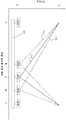
도 3a는 정상(normal) 및 경사 조명을 갖는 예시적인 검사 시스템을 도시한다.
도 3b는 다수의 측정 서브 시스템을 갖는 예시적인 계측 시스템을 도시한다.
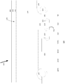
도 4는 본 발명의 일 실시 예에 따른 단순화된 라인 센서를 포함하는 예시적인 검사 시스템을 도시한다.
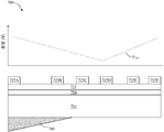
도 5a, 도 5b, 도 5c 및 도 5d는 본 발명의 대안적인 실시 예들에 따른 저항성 제어 게이트에 인가될 수 있는 예시적인 전압 프로파일을 도시한다.
도 6은 본 발명의 다른 특정한 실시 예에 따른 예시적인 라인 센서의 픽셀을 도시한 단면도이다.
도 7은 본 발명의 다른 특정한 실시 예에 따른 예시적인 라인 센서의 단순화된 픽셀을 도시한 단면도이다.
Claims (23)
- 샘플을 검사하는 방법에 있어서,
상기 샘플 상으로 방사선을 지향시키고 집속시키는 단계;
상기 샘플로부터 수신된 방사선을 라인 센서에 지향시키는 단계로서, 상기 라인 센서는 기판 상에 배치된 복수의 픽셀들을 포함하고, 각 픽셀은 상기 기판의 상부 표면에 부착되고 상기 픽셀의 관련된 광 감응(light sensitive) 영역 위(over)에 배치된 저항성 제어 게이트(resistive control gate)를 포함하며, 상기 수신된 방사선 지향 단계는 상기 지향된 광이 상기 복수의 픽셀들 각각의 관련된 광 감응 영역으로 들어가게 하는 단계를 포함하는 것인, 상기 수신된 방사선 지향 단계; 및
상기 저항성 제어 게이트가 각 상기 픽셀의 제1 광 감응 부분에서 제1 광 부분들에 의해 생성된 제1 광전자들을 각 상기 저항성 제어 게이트의 제1 단부에 인접하여 위치한 제1 전하 축적 영역 내로 드라이브(drive)하고, 각 상기 픽셀의 제2 광 감응 부분에서 제2 광 부분들에 의해 생성된 제2 광전자들을 각 상기 저항성 제어 게이트의 제2 단부에 인접하여 위치한 제2 전하 축적 영역 내로 드라이브하는, 상기 관련된 광 감응 영역 내에 전기장을 생성하도록, 미리 결정된 애퍼처 제어 신호들을 사용하여 각 상기 픽셀의 저항성 제어 게이트를 드라이브하는 단계를 포함하는 것인 샘플 검사 방법. - 제1항에 있어서, 미리 결정된 기간 동안 상기 제1 전하 축적 영역 내에 축적된 상기 제1 광전자들을 측정하는 단계를 더 포함하는 것인 샘플 검사 방법.
- 제2항에 있어서, 상기 방사선을 지향시키는 단계는,
상기 샘플로부터 각 상기 픽셀의 상기 관련된 광 감응 영역의 제1 광 감응 부분 내로 지향되는 제1 공초점(confocal) 이미지 부분들, 및 상기 샘플로부터 각 상기 픽셀의 상기 관련된 광 감응 영역의 제2 광 감응 부분 내로 지향되는 제1 공초점 이미지 부분들을 포함하는 공초점 이미지를 생성하는 단계를 더 포함하는 것인 샘플 검사 방법. - 제2항에 있어서, 상기 방사선을 지향시키는 단계는,
상기 샘플로부터 제1 각도 범위 내에 배치된 제1 방사선 부분들을 각 상기 픽셀의 상기 관련된 광 감응 영역의 제1 광 감응 부분 내로 지향시키는 단계, 및 상기 샘플로부터 제2 각도 범위 내에 배치된 제2 방사선 부분들을 각 상기 픽셀의 상기 관련된 광 감응 영역의 제2 광 감응 부분 내로 지향시키는 단계를 더 포함하는 것인 샘플 검사 방법. - 제1항에 있어서, 각 상기 픽셀의 상기 저항성 제어 게이트를 드라이브하는 단계는,
각 상기 저항성 제어 게이트의 대향 단부들과 접촉하는 제1 및 제2 단부 전극 상에 제1 및 제2 애퍼처 제어 신호를 생성하는 단계, 및 각 상기 저항성 제어 게이트의 중심 부분과 접촉하는 적어도 하나의 중심 전극 상에 제3 애퍼처 제어 신호를 생성하는 단계를 더 포함하는 것인 샘플 검사 방법. - 제5항에 있어서, 상기 저항성 제어 게이트를 드라이브하는 단계는,
제1 기간 동안, 상기 제1 및 제2 애퍼처 제어 신호가 상기 제3 애퍼처 제어 신호보다 더 포지티브하도록 상기 제1, 제2, 제3 제어 신호를 생성하는 단계; 및
제2 기간 동안, 상기 제1 제어 신호가 상기 제2 및 제3 제어 신호보다 더 포지티브하도록 상기 제1, 제2, 제3 제어 신호를 생성하는 단계를 더 포함하는 것인 샘플 검사 방법. - 제1항에 있어서, 각 상기 픽셀의 저항성 제어 게이트를 드라이브하는 단계는,
각 상기 저항성 제어 게이트의 대응 단부에 각각 접촉하는 제1 및 제2 단부 전극 상에 제1 및 제2 애퍼처 제어 신호를 생성하는 단계, 및
각 상기 저항성 제어 게이트의 대응 중심 부분에 각각 접촉하는 제1, 제2 및 제3 중심 전극 상에 각각 제3, 제4, 제5 애퍼처 제어 신호를 생성하는 단계를 포함하고,
상기 제1, 제2 및 제4 애퍼처 제어 신호는 상기 제3 및 제5 애퍼처 제어 신호보다 더 포지티브하고, 이에 의해, 각 상기 픽셀의 상기 저항성 제어 게이트는, 상기 제1 광전자들을 상기 제1 전자 축적 영역 내로 드라이브하고, 상기 제2 광전자들을 상기 제2 전하 축적 영역 내로 드라이브하고, 각 상기 픽셀의 제3 광 감응 부분에서 제3 광 부분에 의해 생성된 제3 광전자들을 상기 제1 및 제2 전하 축적 영역 사이에 위치한 제3 전하 축적 영역 내로 드라이브하는 상기 관련된 광 감응 영역 내에 전기장을 생성하는 것인 샘플 검사 방법. - 제7항에 있어서, 상기 방사선을 지향시키는 단계는,
제1 각도 범위 내에 배치된 제1 방사선 부분을 상기 샘플로부터 각 상기 픽셀의 상기 관련된 광 감응 영역의 상기 제1 광 감응 부분 내로 지향시키는 단계,
제2 각도 범위 내에 배치된 제2 방사선 부분을 상기 샘플로부터 각 상기 픽셀의 상기 관련된 광 감응 영역의 상기 제2 광 감응 부분 내로 지향시키는 단계, 및
제3 각도 범위 내에 배치된 제3 방사선 부분을 상기 샘플로부터 각 상기 픽셀의 상기 관련된 광 감응 영역의 상기 제3 광 감응 부분 내로 지향시키는 단계를 포함하는 것인 샘플 검사 방법. - 제1항에 있어서,
상기 라인 센서는 상기 기판의 하부 표면(lower surface)과 상기 샘플 사이에 배치된 기계적 애퍼처 구조를 포함하고,
상기 저항성 제어 게이트를 드라이브하는 단계는, 상기 전기장을 조정하여 상기 기계적 애퍼처 구조의 오정렬을 보정하는 단계를 포함하는 것인 샘플 검사 방법. - 센서에 있어서,
상부 표면(upper surface) 및 대향하는 하부 표면을 갖는 기판;
상기 기판 상에 배치된 복수의 픽셀들로서, 각 픽셀은 상기 상부 표면에 부착되고 상기 픽셀의 관련된 광 감응 영역 위에 배치된 저항성 제어 게이트, 상기 저항성 제어 게이트의 제1 단부에 인접하여 배치된 제1 전송 게이트(transfer gate), 및 상기 저항성 제어 게이트의 제2 단부에 인접하여 배치된 제2 전송 게이트를 포함하는, 상기 복수의 픽셀들;
상기 복수의 픽셀들의 상기 저항성 제어 게이트들을 가로질러 평행하게 연장되고, 각 상기 저항성 제어 게이트의 상기 제1 단부에 접촉하는 제1 단부 전극, 각 상기 저항성 제어 게이트의 상기 제2 단부에 접촉하는 제2 단부 전극, 및 상기 제1 및 제2 단부 전극 사이에 배치되고, 각 상기 저항성 제어 게이트에 접촉하는 하나 이상의 중심 전극을 포함하는, 복수의 길쭉한(elongated) 애퍼처 제어 전극들; 및
상기 제1 및 제2 단부 전극에 인가되는 제1 및 제2 애퍼처 제어 신호가 상기 적어도 하나의 중심 전극에 인가되는 제3 애퍼처 제어 신호보다 더 포지티브하도록, 상기 복수의 애퍼처 제어 전극들을 통하여 상기 복수의 픽셀들의 상기 저항성 제어 게이트들에 애퍼처 제어 신호들을 동시에 인가하도록 구성된 제어 회로로서, 이에 의해 각 상기 픽셀의 제1 광 감응 부분에서 상기 제1 광 부분에 의해 생성되는 제1 광전자들이 각 상기 저항성 제어 게이트의 상기 제1 단부에 인접하여 위치한 제1 전하 축적 영역 내로 상기 전기장에 의해 드라이브되도록 그리고 각 상기 픽셀의 상기 제2 광 감응 부분에서 제2 광 부분에 의해 생성되는 제2 광전자들이 각 상기 저항성 제어 게이트의 상기 제2 단부에 인접하여 위치한 제2 전하 축적 영역 내로 상기 전기장에 의해 드라이브되도록, 각 상기 저항성 제어 게이트가 상기 관련된 광 감응 영역 내에 전기장을 생성하게 하는 상기 제어 회로를 포함하는 것인 센서. - 제10항에 있어서,
복수의 판독(readout) 레지스터들을 포함하는 판독 회로를 더 포함하고,
각 상기 판독 회로는 상기 복수의 픽셀들 중 관련된 픽셀의 상기 제1 전송 게이트에 동작 가능하게 결합되고,
상기 제어 회로는 또한, 판독 동작 동안 상기 제1 광전자들이 상기 복수의 픽셀들의 상기 제1 전송 게이트들을 통하여 상기 제1 전하 축적 영역들로부터 상기 복수의 판독 레지스터들로 전송되도록, 상기 복수의 픽셀들 및 상기 판독 회로를 작동시키도록(actuate) 구성되는 것인 센서. - 제10항에 있어서, 상기 하나 이상의 중심 전극은 적어도 3개의 중심 전극을 포함하고,
상기 제어 회로는 또한, 각 상기 픽셀의 제3 광 감응 부분에서 제3 광 부분에 의해 생성되는 제3 광전자들이 상기 전기장에 의해 상기 제1 및 제2 전하 축적 영역 사이에 위치한 제3 전하 축적 영역 내로 드라이브되도록 상기 애퍼처 제어 신호들을 생성하도록 구성되는 것인 센서. - 제10항에 있어서, 상기 기판은 에피택셜 실리콘 층을 포함하고, 상기 센서는 상기 에피택셜 실리콘 층의 하부 표면 위에(over) 형성된 순수한 붕소 층을 더 포함하는 것인 센서.
- 제10항에 있어서, 상기 기판은 에피택셜 실리콘 층을 포함하고, 상기 센서는 상기 에피택셜 실리콘 층의 하부 표면 위에(over) 형성된 반사 방지층(anti-reflection layer)을 더 포함하는 것인 센서.
- 샘플을 검사 또는 측정하기 위한 시스템에 있어서,
광을 생성하도록 구성된 조명원;
상기 조명원으로부터 상기 샘플로 상기 광을 지향시키고, 상기 샘플로부터의 광을 센서로 지향시키는 광학 기기(optics); 및
센서를 포함하고,
상기 센서는,
상부 표면 및 대향하는 하부 표면을 갖는 기판;
상기 기판 상에 배치된 복수의 픽셀들로서, 각 픽셀이 상기 상부 표면에 부착되고 상기 픽셀의 관련된 광 감응 영역 위에 배치된 저항성 제어 게이트를 포함하는, 상기 복수의 픽셀들;
상기 복수의 픽셀들의 각각의 상기 저항성 제어 게이트를 가로질러 연장되고, 상기 저항성 제어 게이트에 전기적으로 접속되고, 각 상기 저항성 제어 게이트의 대향하는 제1 및 제2 단부를 가로질러 각각 연장되는 제1 및 제2 단부 전극, 및 상기 제1 및 제2 단부 전극 사이에 배치되는 하나 이상의 중심 전극을 포함하는, 적어도 3개의 애퍼처 제어 전극들; 및
각 상기 저항성 제어 게이트가 상기 관련된 광 감응 영역으로 들어오는 광에 의해 생성되는 광전자들을 적어도 2개의 부분으로 분리하는 상기 관련된 광 감응 영역 내에 전기장을 생성하도록, 상기 적어도 3개의 애퍼처 제어 전극을 통하여 상기 복수의 픽셀들의 상기 저항성 제어 게이트 위로 애퍼처 제어 신호들을 동시에 인가하도록 구성된 제어 회로를 포함하는 것인,
샘플 검사 또는 측정 시스템. - 제15항에 있어서, 상기 센서는 상기 복수의 픽셀들의 대향 측면들 상에 각각 배치된 제1 및 제2 판독 회로를 포함하는 것인, 샘플 검사 또는 측정 시스템.
- 제16항에 있어서,
상기 하나 이상의 중심 전극은 복수의 중심 전극들을 포함하고,
상기 제어 회로는 상기 애퍼처 제어 신호들의 다수의 조합을 생성하여, 하나의 상기 조합으로부터 다른 상기 조합으로 변경됨으로써 상기 전기장이 조정 가능하도록 구성되는 것인, 샘플 검사 또는 측정 시스템. - 제16항에 있어서,
상기 하나 이상의 중심 전극은 적어도 3개의 중심 전극을 포함하고,
상기 제어 회로는 상기 광전자들이 적어도 3개의 부분으로 분할(divide)되도록 상기 애퍼처 제어 신호들을 생성하도록 구성되는 것인 샘플 검사 또는 측정 시스템. - 제18항에 있어서,
상기 광학 기기는 또한, 제1 각도 범위 내에서 상기 샘플로부터 상기 센서로 지향된 제1 광 부분이 각 상기 픽셀의 상기 관련된 광 감응 영역의 제1 광 감응 부분 내로 지향되도록, 그리고 제2 각도 범위 내에서 상기 샘플로부터 상기 센서로 지향된 제2 광 부분이 각 상기 픽셀의 상기 관련된 광 감응 영역의 제2 광 감응 부분 내로 지향되도록 구성되고,
상기 저항성 제어 게이트는, 각 상기 픽셀의 상기 제1 광 감응 부분에서 상기 제1 광 부분에 의해 생성되는 제1 광전자들이 각 상기 저항성 제어 게이트의 상기 제1 단부에 인접하여 위치한 제1 전하 축적 영역 내로 상기 전기장에 의해 드라이브되도록 그리고 각 상기 픽셀의 상기 제2 광 감응 부분에서 상기 제2 광 부분에 의해 생성되는 제2 광전자들이 각 상기 저항성 제어 게이트의 상기 제2 단부에 인접하여 위치한 제2 전하 축적 영역 내로 상기 전기장에 의해 바이어스되도록, 상기 전기장을 생성하는 것인 샘플 검사 또는 측정 시스템. - 제15항에 있어서, 상기 기판은 반도체 멤브레인을 포함하고, 상기 센서는 상기 반도체 멤브레인의 하부 표면 상에 증착된 순수 붕소 층을 더 포함하는 것인 샘플 검사 또는 측정 시스템.
- 제15항에 있어서, 상기 기판은 반도체 멤브레인을 포함하고, 상기 센서는 상기 반도체 멤브레인의 하부 표면 상에 증착된 반사 방지층을 더 포함하는 것인 샘플 검사 또는 측정 시스템.
- 제15항에 있어서, 상기 시스템은 상기 샘플로부터 광을 수신하도록 구성된 적어도 2개의 센서를 포함하는 것인 샘플 검사 또는 측정 시스템.
- 제15항에 있어서, 기계적 애퍼처 구조를 더 포함하고,
상기 기계적 애퍼처 구조는 상기 샘플로부터의 광의 일부가 상기 기계적 애퍼처 구조에 의해 차단되도록 상기 기판의 하부 표면에 인접하여 배치되고,
상기 제어 회로는 또한, 상기 센서에 대한 상기 기계적 애퍼처 구조의 오정렬에 따라 상기 전기장을 조정하도록 구성되는 것인 샘플 검사 또는 측정 시스템.
Applications Claiming Priority (7)
| Application Number | Priority Date | Filing Date | Title |
|---|---|---|---|
| US201562161450P | 2015-05-14 | 2015-05-14 | |
| US62/161,450 | 2015-05-14 | ||
| US201562172242P | 2015-06-08 | 2015-06-08 | |
| US62/172,242 | 2015-06-08 | ||
| US15/153,543 US9860466B2 (en) | 2015-05-14 | 2016-05-12 | Sensor with electrically controllable aperture for inspection and metrology systems |
| US15/153,543 | 2016-05-12 | ||
| PCT/US2016/032378 WO2016183451A1 (en) | 2015-05-14 | 2016-05-13 | Sensor with electrically controllable aperture for inspection and metrology systems |
Publications (2)
| Publication Number | Publication Date |
|---|---|
| KR20170141806A true KR20170141806A (ko) | 2017-12-26 |
| KR102284002B1 KR102284002B1 (ko) | 2021-07-29 |
Family
ID=57249396
Family Applications (1)
| Application Number | Title | Priority Date | Filing Date |
|---|---|---|---|
| KR1020177035444A Active KR102284002B1 (ko) | 2015-05-14 | 2016-05-13 | 검사 및 계측 시스템을 위한 전기적으로 제어 가능한 애퍼처를 갖춘 센서 |
Country Status (7)
| Country | Link |
|---|---|
| US (2) | US9860466B2 (ko) |
| JP (2) | JP6682558B2 (ko) |
| KR (1) | KR102284002B1 (ko) |
| CN (2) | CN107548554B (ko) |
| IL (1) | IL255230B (ko) |
| TW (1) | TWI692628B (ko) |
| WO (1) | WO2016183451A1 (ko) |
Cited By (1)
| Publication number | Priority date | Publication date | Assignee | Title |
|---|---|---|---|---|
| US10892145B2 (en) | 2018-11-22 | 2021-01-12 | Samsung Electronics Co., Ltd. | Substrate processing apparatus, substrate processing method, and method of fabricating semiconductor device using the same |
Families Citing this family (19)
| Publication number | Priority date | Publication date | Assignee | Title |
|---|---|---|---|---|
| US9860466B2 (en) * | 2015-05-14 | 2018-01-02 | Kla-Tencor Corporation | Sensor with electrically controllable aperture for inspection and metrology systems |
| JP6279013B2 (ja) * | 2016-05-26 | 2018-02-14 | Ckd株式会社 | 三次元計測装置 |
| US11662646B2 (en) | 2017-02-05 | 2023-05-30 | Kla Corporation | Inspection and metrology using broadband infrared radiation |
| CN109425619B (zh) * | 2017-08-31 | 2021-12-28 | 深圳中科飞测科技股份有限公司 | 光学测量系统及方法 |
| JP2019191168A (ja) * | 2018-04-23 | 2019-10-31 | ブルカー ジェイヴィ イスラエル リミテッドBruker Jv Israel Ltd. | 小角x線散乱測定用のx線源光学系 |
| KR102139988B1 (ko) * | 2018-07-12 | 2020-07-31 | 한국표준과학연구원 | 수직입사 타원계측기 및 이를 이용한 시편의 광물성 측정 방법 |
| US11703464B2 (en) | 2018-07-28 | 2023-07-18 | Bruker Technologies Ltd. | Small-angle x-ray scatterometry |
| US10705026B2 (en) * | 2018-10-26 | 2020-07-07 | Kla Corporation | Scanning differential interference contrast in an imaging system design |
| CN109297991B (zh) * | 2018-11-26 | 2019-12-17 | 深圳市麓邦技术有限公司 | 一种玻璃表面缺陷检测系统及方法 |
| US10921261B2 (en) * | 2019-05-09 | 2021-02-16 | Kla Corporation | Strontium tetraborate as optical coating material |
| JP2020204579A (ja) | 2019-06-18 | 2020-12-24 | 住友電工デバイス・イノベーション株式会社 | ウェハの表面検査方法、表面検査装置、および電子部品の製造方法 |
| CN110632973B (zh) * | 2019-09-24 | 2021-07-09 | 中国航空工业集团公司沈阳飞机设计研究所 | 一种电磁辐射控制方法及其装置 |
| CN111229335B (zh) * | 2020-01-17 | 2021-11-30 | 上海新微技术研发中心有限公司 | 光波导微流体芯片的制造方法 |
| US12196673B2 (en) | 2020-03-31 | 2025-01-14 | Hitachi High-Tech Corporation | Defect inspection apparatus and defect inspection method |
| CN112665514B (zh) * | 2021-01-11 | 2022-09-20 | 成都工业职业技术学院 | 一种自动定心、高速检测机械零件孔间距的装置 |
| US11781999B2 (en) | 2021-09-05 | 2023-10-10 | Bruker Technologies Ltd. | Spot-size control in reflection-based and scatterometry-based X-ray metrology systems |
| US20240402094A1 (en) * | 2021-10-05 | 2024-12-05 | Ehwa Diamond Industrial Company Limited | Method for measuring depth of damaged layer and concentration of defects in damaged layer, and system for performing same method |
| US12249059B2 (en) | 2022-03-31 | 2025-03-11 | Bruker Technologies Ltd. | Navigation accuracy using camera coupled with detector assembly |
| KR102942298B1 (ko) | 2023-10-11 | 2026-03-20 | 한국식품연구원 | 라인빔 생성모듈 및 이를 포함하는 라인스캔 검사장치 |
Citations (4)
| Publication number | Priority date | Publication date | Assignee | Title |
|---|---|---|---|---|
| US6064759A (en) * | 1996-11-08 | 2000-05-16 | Buckley; B. Shawn | Computer aided inspection machine |
| US20130009069A1 (en) * | 2011-07-07 | 2013-01-10 | Fujifilm Corporation | Radiation detector, radiographic imaging device and radiographic imaging system |
| US20130176552A1 (en) * | 2011-09-21 | 2013-07-11 | Kla-Tencor Corporation | Interposer based imaging sensor for high-speed image acquisition and inspection systems |
| US20130336574A1 (en) * | 2012-06-14 | 2013-12-19 | Kla-Tencor Corporation | Apparatus and methods for inspecting extreme ultra violet reticles |
Family Cites Families (249)
| Publication number | Priority date | Publication date | Assignee | Title |
|---|---|---|---|---|
| US3870917A (en) | 1971-05-10 | 1975-03-11 | Itt | Discharge device including channel type electron multiplier having ion adsorptive layer |
| GB1444951A (en) | 1973-06-18 | 1976-08-04 | Mullard Ltd | Electronic solid state devices |
| GB1536412A (en) | 1975-05-14 | 1978-12-20 | English Electric Valve Co Ltd | Photocathodes |
| US4210922A (en) | 1975-11-28 | 1980-07-01 | U.S. Philips Corporation | Charge coupled imaging device having selective wavelength sensitivity |
| NL7611593A (nl) | 1976-10-20 | 1978-04-24 | Optische Ind De Oude Delft Nv | Werkwijze voor het in een beeldversterkerbuis aanbrengen van een lichtabsorberende, voor elek- tronen doorlaatbare laag. |
| US4106046A (en) | 1977-01-26 | 1978-08-08 | Westinghouse Electric Corp. | Radiant energy sensor |
| US4280141A (en) | 1978-09-22 | 1981-07-21 | Mccann David H | Time delay and integration detectors using charge transfer devices |
| JPS58146B2 (ja) | 1980-10-14 | 1983-01-05 | 浜松テレビ株式会社 | フレ−ミング管 |
| US4348690A (en) | 1981-04-30 | 1982-09-07 | Rca Corporation | Semiconductor imagers |
| US4644221A (en) | 1981-05-06 | 1987-02-17 | The United States Of America As Represented By The Secretary Of The Army | Variable sensitivity transmission mode negative electron affinity photocathode |
| US4382267A (en) | 1981-09-24 | 1983-05-03 | Rca Corporation | Digital control of number of effective rows of two-dimensional charge-transfer imager array |
| US4580155A (en) | 1982-12-21 | 1986-04-01 | Northern Telecom Limited | Deep depletion CCD imager |
| US4555731A (en) | 1984-04-30 | 1985-11-26 | Polaroid Corporation | Electronic imaging camera with microchannel plate |
| US4760031A (en) | 1986-03-03 | 1988-07-26 | California Institute Of Technology | Producing CCD imaging sensor with flashed backside metal film |
| US4853595A (en) | 1987-08-31 | 1989-08-01 | Alfano Robert R | Photomultiplier tube having a transmission strip line photocathode and system for use therewith |
| US5483378A (en) | 1988-04-19 | 1996-01-09 | Litton Systems, Inc. | Fault tolerant anti-reflective coatings |
| US4999014A (en) | 1989-05-04 | 1991-03-12 | Therma-Wave, Inc. | Method and apparatus for measuring thickness of thin films |
| NL8902271A (nl) | 1989-09-12 | 1991-04-02 | Philips Nv | Werkwijze voor het verbinden van twee lichamen. |
| US5120949A (en) | 1991-01-17 | 1992-06-09 | Burle Technologies, Inc. | Semiconductor anode photomultiplier tube |
| US5144630A (en) | 1991-07-29 | 1992-09-01 | Jtt International, Inc. | Multiwavelength solid state laser using frequency conversion techniques |
| US5563702A (en) | 1991-08-22 | 1996-10-08 | Kla Instruments Corporation | Automated photomask inspection apparatus and method |
| US5440648A (en) | 1991-11-19 | 1995-08-08 | Dalsa, Inc. | High speed defect detection apparatus having defect detection circuits mounted in the camera housing |
| US5181080A (en) | 1991-12-23 | 1993-01-19 | Therma-Wave, Inc. | Method and apparatus for evaluating the thickness of thin films |
| US5376810A (en) | 1992-06-26 | 1994-12-27 | California Institute Of Technology | Growth of delta-doped layers on silicon CCD/S for enhanced ultraviolet response |
| US5227313A (en) | 1992-07-24 | 1993-07-13 | Eastman Kodak Company | Process for making backside illuminated image sensors |
| US5315126A (en) | 1992-10-13 | 1994-05-24 | Itt Corporation | Highly doped surface layer for negative electron affinity devices |
| US5428392A (en) | 1992-11-20 | 1995-06-27 | Picker International, Inc. | Strobing time-delayed and integration video camera system |
| US5475227A (en) | 1992-12-17 | 1995-12-12 | Intevac, Inc. | Hybrid photomultiplier tube with ion deflector |
| US5326978A (en) | 1992-12-17 | 1994-07-05 | Intevac, Inc. | Focused electron-bombarded detector |
| US5760809A (en) | 1993-03-19 | 1998-06-02 | Xerox Corporation | Recording sheets containing phosphonium compounds |
| FI940740A0 (fi) | 1994-02-17 | 1994-02-17 | Arto Salokatve | Detektor foer paovisning av fotoner eller partiklar, foerfarande foer framstaellning av detektorn och maetningsfoerfarande |
| US6271916B1 (en) | 1994-03-24 | 2001-08-07 | Kla-Tencor Corporation | Process and assembly for non-destructive surface inspections |
| US5493176A (en) | 1994-05-23 | 1996-02-20 | Siemens Medical Systems, Inc. | Photomultiplier tube with an avalanche photodiode, a flat input end and conductors which simulate the potential distribution in a photomultiplier tube having a spherical-type input end |
| US5684583A (en) | 1994-06-27 | 1997-11-04 | The Furukawa Electric Co., Ltd. | Apparatus for detecting foreign matter in a fluid |
| US20080315092A1 (en) | 1994-07-28 | 2008-12-25 | General Nanotechnology Llc | Scanning probe microscopy inspection and modification system |
| EP0702221A3 (en) | 1994-09-14 | 1997-05-21 | Delco Electronics Corp | Sensor integrated on a chip |
| US5608526A (en) | 1995-01-19 | 1997-03-04 | Tencor Instruments | Focused beam spectroscopic ellipsometry method and system |
| JPH08241977A (ja) | 1995-03-03 | 1996-09-17 | Hamamatsu Photonics Kk | 半導体装置の製造方法 |
| FR2733111B1 (fr) | 1995-04-11 | 1997-05-23 | Thomson Csf | Procede de detection a cycles d'integration et de lecture repartis pour camera a balayage, et barrette de detection correspondante |
| WO1996036999A1 (de) | 1995-05-19 | 1996-11-21 | Dr. Johannes Heidenhain Gmbh | Strahlungsempfindliches detektorelement und verfahren zur herstellung desselben |
| JP3405620B2 (ja) | 1995-05-22 | 2003-05-12 | 松下電器産業株式会社 | 固体撮像装置 |
| US5731584A (en) | 1995-07-14 | 1998-03-24 | Imec Vzw | Position sensitive particle sensor and manufacturing method therefor |
| US6362484B1 (en) | 1995-07-14 | 2002-03-26 | Imec Vzw | Imager or particle or radiation detector and method of manufacturing the same |
| US5754228A (en) * | 1995-09-25 | 1998-05-19 | Lockhead Martin Corporation | Rapid-sequence full-frame CCD sensor |
| US6081325A (en) | 1996-06-04 | 2000-06-27 | Kla-Tencor Corporation | Optical scanning system for surface inspection |
| US5717518A (en) | 1996-07-22 | 1998-02-10 | Kla Instruments Corporation | Broad spectrum ultraviolet catadioptric imaging system |
| US5999310A (en) | 1996-07-22 | 1999-12-07 | Shafer; David Ross | Ultra-broadband UV microscope imaging system with wide range zoom capability |
| US5877859A (en) | 1996-07-24 | 1999-03-02 | Therma-Wave, Inc. | Broadband spectroscopic rotating compensator ellipsometer |
| US5742626A (en) | 1996-08-14 | 1998-04-21 | Aculight Corporation | Ultraviolet solid state laser, method of using same and laser surgery apparatus |
| US5760899A (en) | 1996-09-04 | 1998-06-02 | Erim International, Inc. | High-sensitivity multispectral sensor |
| US5940685A (en) | 1996-10-28 | 1999-08-17 | The United States Of America As Represented By The Secretary Of The Air Force | Fabrication of UV-sensitive back illuminated CCD image sensors |
| JPH10171965A (ja) | 1996-12-05 | 1998-06-26 | Toshiba Corp | 積算型エリアセンサの画像入力方法及びその装置 |
| AU6178398A (en) | 1997-02-21 | 1998-09-09 | Board Of Regents Of The University And Community College System Of Nevada, The | Method and system for computerized high-rate image processing |
| DE19714221A1 (de) | 1997-04-07 | 1998-10-08 | Zeiss Carl Fa | Konfokales Mikroskop mit einem motorischen Scanningtisch |
| US5965910A (en) | 1997-04-29 | 1999-10-12 | Ohmeda Inc. | Large cell charge coupled device for spectroscopy |
| US6278519B1 (en) | 1998-01-29 | 2001-08-21 | Therma-Wave, Inc. | Apparatus for analyzing multi-layer thin film stacks on semiconductors |
| US6107619A (en) | 1997-07-14 | 2000-08-22 | California Institute Of Technology | Delta-doped hybrid advanced detector for low energy particle detection |
| US6608676B1 (en) | 1997-08-01 | 2003-08-19 | Kla-Tencor Corporation | System for detecting anomalies and/or features of a surface |
| US6201601B1 (en) | 1997-09-19 | 2001-03-13 | Kla-Tencor Corporation | Sample inspection system |
| US6403963B1 (en) | 1997-09-29 | 2002-06-11 | California Institute Of Technology | Delta-doped CCD's as low-energy particle detectors and imagers |
| US6278119B1 (en) | 1997-10-21 | 2001-08-21 | California Institute Of Technology | Using a delta-doped CCD to determine the energy of a low-energy particle |
| JPH11153516A (ja) | 1997-11-21 | 1999-06-08 | Toppan Printing Co Ltd | 画像撮像装置 |
| US6297879B1 (en) | 1998-02-27 | 2001-10-02 | Micron Technology, Inc. | Inspection method and apparatus for detecting defects on photomasks |
| JP2882409B1 (ja) | 1998-04-24 | 1999-04-12 | 株式会社東京精密 | 外観検査装置 |
| US6162707A (en) | 1998-05-18 | 2000-12-19 | The Regents Of The University Of California | Low work function, stable thin films |
| DE19829172A1 (de) | 1998-06-30 | 2000-01-05 | Univ Konstanz | Verfahren zur Herstellung von Antireflexschichten |
| US6373869B1 (en) | 1998-07-30 | 2002-04-16 | Actinix | System and method for generating coherent radiation at ultraviolet wavelengths |
| US9029793B2 (en) | 1998-11-05 | 2015-05-12 | Siemens Aktiengesellschaft | Imaging device |
| US6013399A (en) | 1998-12-04 | 2000-01-11 | Advanced Micro Devices, Inc. | Reworkable EUV mask materials |
| US6867406B1 (en) | 1999-03-23 | 2005-03-15 | Kla-Tencor Corporation | Confocal wafer inspection method and apparatus using fly lens arrangement |
| US7339568B2 (en) * | 1999-04-16 | 2008-03-04 | Samsung Electronics Co., Ltd. | Signal transmission film and a liquid crystal display panel having the same |
| US6535531B1 (en) | 2001-11-29 | 2003-03-18 | Cymer, Inc. | Gas discharge laser with pulse multiplier |
| US6657178B2 (en) | 1999-07-20 | 2003-12-02 | Intevac, Inc. | Electron bombarded passive pixel sensor imaging |
| US6307586B1 (en) | 1999-07-20 | 2001-10-23 | Intevac, Inc. | Electron bombarded active pixel sensor camera incorporating gain control |
| US6285018B1 (en) | 1999-07-20 | 2001-09-04 | Intevac, Inc. | Electron bombarded active pixel sensor |
| WO2001008224A1 (en) * | 1999-07-26 | 2001-02-01 | Edge Medical Devices Ltd. | Digital detector for x-ray imaging |
| US6429943B1 (en) | 2000-03-29 | 2002-08-06 | Therma-Wave, Inc. | Critical dimension analysis with simultaneous multiple angle of incidence measurements |
| US6711283B1 (en) | 2000-05-03 | 2004-03-23 | Aperio Technologies, Inc. | Fully automatic rapid microscope slide scanner |
| JP2002033473A (ja) | 2000-07-17 | 2002-01-31 | Hamamatsu Photonics Kk | 半導体装置 |
| US6879390B1 (en) | 2000-08-10 | 2005-04-12 | Kla-Tencor Technologies Corporation | Multiple beam inspection apparatus and method |
| US6507147B1 (en) | 2000-08-31 | 2003-01-14 | Intevac, Inc. | Unitary vacuum tube incorporating high voltage isolation |
| US7136159B2 (en) | 2000-09-12 | 2006-11-14 | Kla-Tencor Technologies Corporation | Excimer laser inspection system |
| US7046283B1 (en) | 2000-10-11 | 2006-05-16 | Dalsa, Inc. | Arrangements of clock line drivers |
| JP2002184302A (ja) | 2000-12-18 | 2002-06-28 | Hamamatsu Photonics Kk | 半導体光電陰極 |
| KR20020084541A (ko) | 2001-05-02 | 2002-11-09 | (주)한비젼 | 이동형 단말기기에 적용 가능한 초박형 영상모듈의 구현 |
| US7009163B2 (en) | 2001-06-22 | 2006-03-07 | Orbotech Ltd. | High-sensitivity optical scanning using memory integration |
| US6545281B1 (en) | 2001-07-06 | 2003-04-08 | The United States Of America As Represented By The United States Department Of Energy | Pocked surface neutron detector |
| JP3573725B2 (ja) | 2001-08-03 | 2004-10-06 | 川崎重工業株式会社 | X線顕微鏡装置 |
| US6900888B2 (en) | 2001-09-13 | 2005-05-31 | Hitachi High-Technologies Corporation | Method and apparatus for inspecting a pattern formed on a substrate |
| US7015452B2 (en) | 2001-10-09 | 2006-03-21 | Itt Manufacturing Enterprises, Inc. | Intensified hybrid solid-state sensor |
| US6747258B2 (en) | 2001-10-09 | 2004-06-08 | Itt Manufacturing Enterprises, Inc. | Intensified hybrid solid-state sensor with an insulating layer |
| US7233350B2 (en) | 2002-01-05 | 2007-06-19 | Candela Microsystems, Inc. | Image sensor with interleaved image output |
| US6908355B2 (en) | 2001-11-13 | 2005-06-21 | Burle Technologies, Inc. | Photocathode |
| JP4068340B2 (ja) | 2001-12-17 | 2008-03-26 | エルピーダメモリ株式会社 | 半導体集積回路装置 |
| FR2834345B1 (fr) | 2001-12-27 | 2004-03-26 | Essilor Int | Article d'optique comportant une lame quart d'onde et son procede de fabrication |
| US7130039B2 (en) | 2002-04-18 | 2006-10-31 | Kla-Tencor Technologies Corporation | Simultaneous multi-spot inspection and imaging |
| JP4165129B2 (ja) | 2002-06-21 | 2008-10-15 | 三菱電機株式会社 | 裏面入射型固体撮像素子 |
| US7408683B2 (en) | 2002-07-15 | 2008-08-05 | Brother Kogyo Kabushiki Kaisha | Image sensor for reading image and image reading apparatus including the image sensor |
| US20040012684A1 (en) | 2002-07-16 | 2004-01-22 | Fairchild Imaging | Image reconstruction techniques for charge coupled devices |
| US20040021061A1 (en) | 2002-07-30 | 2004-02-05 | Frederik Bijkerk | Photodiode, charged-coupled device and method for the production |
| US7446474B2 (en) | 2002-10-10 | 2008-11-04 | Applied Materials, Inc. | Hetero-junction electron emitter with Group III nitride and activated alkali halide |
| US7283166B1 (en) | 2002-10-15 | 2007-10-16 | Lockheed Martin Corporation | Automatic control method and system for electron bombarded charge coupled device (“EBCCD”) sensor |
| US7126699B1 (en) | 2002-10-18 | 2006-10-24 | Kla-Tencor Technologies Corp. | Systems and methods for multi-dimensional metrology and/or inspection of a specimen |
| US7005637B2 (en) | 2003-01-31 | 2006-02-28 | Intevac, Inc. | Backside thinning of image array devices |
| US6990385B1 (en) | 2003-02-03 | 2006-01-24 | Kla-Tencor Technologies Corporation | Defect detection using multiple sensors and parallel processing |
| GB2398118B (en) | 2003-02-07 | 2006-03-15 | Imp College Innovations Ltd | Photon arrival time detection |
| US7141785B2 (en) | 2003-02-13 | 2006-11-28 | Micromass Uk Limited | Ion detector |
| US7957066B2 (en) | 2003-02-21 | 2011-06-07 | Kla-Tencor Corporation | Split field inspection system using small catadioptric objectives |
| US7227984B2 (en) | 2003-03-03 | 2007-06-05 | Kla-Tencor Technologies Corporation | Method and apparatus for identifying defects in a substrate surface by using dithering to reconstruct under-sampled images |
| JP2005055196A (ja) * | 2003-08-05 | 2005-03-03 | Olympus Corp | 基板検査方法及びその装置 |
| US7813406B1 (en) | 2003-10-15 | 2010-10-12 | The United States Of America As Represented By The Administrator Of The National Aeronautics And Space Administration | Temporal laser pulse manipulation using multiple optical ring-cavities |
| JP2005158780A (ja) | 2003-11-20 | 2005-06-16 | Hitachi Ltd | パターン欠陥検査方法及びその装置 |
| US7023126B2 (en) | 2003-12-03 | 2006-04-04 | Itt Manufacturing Enterprises Inc. | Surface structures for halo reduction in electron bombarded devices |
| JP4311181B2 (ja) | 2003-12-05 | 2009-08-12 | ソニー株式会社 | 半導体装置の制御方法および信号処理方法並びに半導体装置および電子機器 |
| US7321468B2 (en) | 2003-12-15 | 2008-01-22 | Carl Zeiss Laser Optics Gmbh | Method and optical arrangement for beam guiding of a light beam with beam delay |
| JP2005241290A (ja) | 2004-02-24 | 2005-09-08 | Toshiba Corp | 画像入力装置及び検査装置 |
| JP4365255B2 (ja) | 2004-04-08 | 2009-11-18 | 浜松ホトニクス株式会社 | 発光体と、これを用いた電子線検出器、走査型電子顕微鏡及び質量分析装置 |
| US7301263B2 (en) | 2004-05-28 | 2007-11-27 | Applied Materials, Inc. | Multiple electron beam system with electron transmission gates |
| KR100688497B1 (ko) | 2004-06-28 | 2007-03-02 | 삼성전자주식회사 | 이미지 센서 및 그 제조방법 |
| US7141791B2 (en) | 2004-09-07 | 2006-11-28 | Kla-Tencor Technologies Corporation | Apparatus and method for E-beam dark field imaging |
| JP4500641B2 (ja) | 2004-09-29 | 2010-07-14 | 株式会社日立ハイテクノロジーズ | 欠陥検査方法およびその装置 |
| US7455565B2 (en) | 2004-10-13 | 2008-11-25 | The Board Of Trustees Of The Leland Stanford Junior University | Fabrication of group III-nitride photocathode having Cs activation layer |
| JP4185037B2 (ja) | 2004-10-14 | 2008-11-19 | 株式会社東芝 | 欠陥検査装置 |
| US7952633B2 (en) | 2004-11-18 | 2011-05-31 | Kla-Tencor Technologies Corporation | Apparatus for continuous clocking of TDI sensors |
| US7609309B2 (en) | 2004-11-18 | 2009-10-27 | Kla-Tencor Technologies Corporation | Continuous clocking of TDI sensors |
| US7432517B2 (en) | 2004-11-19 | 2008-10-07 | Asml Netherlands B.V. | Pulse modifier, lithographic apparatus, and device manufacturing method |
| WO2006076671A2 (en) | 2005-01-13 | 2006-07-20 | Whitehead Institute For Biomedical Research | Method and apparatus for uv imaging |
| JP4751617B2 (ja) | 2005-01-21 | 2011-08-17 | 株式会社日立ハイテクノロジーズ | 欠陥検査方法及びその装置 |
| JP4713185B2 (ja) | 2005-03-11 | 2011-06-29 | 株式会社日立ハイテクノロジーズ | 異物欠陥検査方法及びその装置 |
| US7485486B2 (en) | 2005-03-18 | 2009-02-03 | Intersil Americas Inc. | Photodiode for multiple wavelength operation |
| DE602006004913D1 (de) | 2005-04-28 | 2009-03-12 | Semiconductor Energy Lab | Verfahren und Vorrichtung zur Herstellung von Halbleitern mittels Laserstrahlung |
| US7531826B2 (en) | 2005-06-01 | 2009-05-12 | Intevac, Inc. | Photocathode structure and operation |
| US7345825B2 (en) | 2005-06-30 | 2008-03-18 | Kla-Tencor Technologies Corporation | Beam delivery system for laser dark-field illumination in a catadioptric optical system |
| US7655493B2 (en) * | 2005-07-14 | 2010-02-02 | Fairchild Imaging, Inc | Multi spectral sensor |
| JP5063875B2 (ja) | 2005-07-27 | 2012-10-31 | パナソニック株式会社 | 光半導体装置の製造方法 |
| JP5403852B2 (ja) | 2005-08-12 | 2014-01-29 | 株式会社荏原製作所 | 検出装置及び検査装置 |
| JP4142734B2 (ja) | 2005-09-16 | 2008-09-03 | 松下電器産業株式会社 | 回折光学素子 |
| JP4925085B2 (ja) | 2005-09-20 | 2012-04-25 | 株式会社メガオプト | 深紫外レーザー光の発生方法および深紫外レーザー装置 |
| WO2007035858A2 (en) | 2005-09-21 | 2007-03-29 | Rjs Technology, Inc. | System and method for a high dynamic range sensitive sensor element or array with gain control |
| JP4939033B2 (ja) | 2005-10-31 | 2012-05-23 | 浜松ホトニクス株式会社 | 光電陰極 |
| JP2007133102A (ja) | 2005-11-09 | 2007-05-31 | Canon Inc | 反射防止膜を有する光学素子及びそれを有する露光装置 |
| US7247835B2 (en) | 2005-12-20 | 2007-07-24 | Keng Yeam Chang | Optical navigation device, and method for manufacturing same |
| US7528943B2 (en) | 2005-12-27 | 2009-05-05 | Kla-Tencor Technologies Corporation | Method and apparatus for simultaneous high-speed acquisition of multiple images |
| JP4888081B2 (ja) | 2006-01-23 | 2012-02-29 | セイコーエプソン株式会社 | 撮像装置、撮像方法、撮像システム及び画像処理装置 |
| KR100768200B1 (ko) | 2006-02-01 | 2007-10-17 | 삼성에스디아이 주식회사 | 광학 필터 및 이를 채용한 플라즈마 디스플레이 패널 |
| JP4992446B2 (ja) | 2006-02-24 | 2012-08-08 | ソニー株式会社 | 固体撮像装置及びその製造方法、並びにカメラ |
| JP2007251463A (ja) | 2006-03-15 | 2007-09-27 | Renesas Technology Corp | 半導体集積回路装置 |
| US7598178B2 (en) | 2006-03-24 | 2009-10-06 | Applied Materials, Inc. | Carbon precursors for use during silicon epitaxial film formation |
| JP5110535B2 (ja) * | 2006-03-31 | 2012-12-26 | 国立大学法人静岡大学 | 半導体測距素子及び固体撮像装置 |
| EP2033036A4 (en) | 2006-06-13 | 2009-07-15 | Invent Technologies Llc | Apparatus and method for deep ultraviolet optical microscopy |
| US7457330B2 (en) | 2006-06-15 | 2008-11-25 | Pavilion Integration Corporation | Low speckle noise monolithic microchip RGB lasers |
| JP4695552B2 (ja) | 2006-06-28 | 2011-06-08 | 富士フイルム株式会社 | 画像処理装置及び方法 |
| US8482197B2 (en) | 2006-07-05 | 2013-07-09 | Hamamatsu Photonics K.K. | Photocathode, electron tube, field assist type photocathode, field assist type photocathode array, and field assist type electron tube |
| US7791170B2 (en) | 2006-07-10 | 2010-09-07 | Taiwan Semiconductor Manufacturing Company, Ltd. | Method of making a deep junction for electrical crosstalk reduction of an image sensor |
| US20080068593A1 (en) | 2006-09-13 | 2008-03-20 | Hiroyuki Nakano | Method and apparatus for detecting defects |
| JP2008096430A (ja) | 2006-09-13 | 2008-04-24 | Hitachi High-Technologies Corp | 欠陥検査方法およびその装置 |
| US7817197B2 (en) | 2006-09-21 | 2010-10-19 | Mediatek Singapore Pte Ltd | Optical black calibration |
| US7800040B2 (en) | 2006-09-21 | 2010-09-21 | California Institute Of Technology | Method for growing a back surface contact on an imaging detector used in conjunction with back illumination |
| US7675561B2 (en) | 2006-09-28 | 2010-03-09 | Cypress Semiconductor Corporation | Time delayed integration CMOS image sensor with zero desynchronization |
| KR100826407B1 (ko) | 2006-10-12 | 2008-05-02 | 삼성전기주식회사 | 자외선 수광용 포토 다이오드 및 이를 포함하는 이미지센서 |
| KR100874954B1 (ko) | 2006-12-04 | 2008-12-19 | 삼성전자주식회사 | 후면 수광 이미지 센서 |
| US20080173903A1 (en) | 2006-12-28 | 2008-07-24 | Fujifilm Corporation | Solid-state image pickup element |
| JP5342769B2 (ja) | 2006-12-28 | 2013-11-13 | 浜松ホトニクス株式会社 | 光電陰極、電子管及び光電子増倍管 |
| JP4742057B2 (ja) * | 2007-02-21 | 2011-08-10 | 富士フイルム株式会社 | 裏面照射型固体撮像素子 |
| JP2008224303A (ja) | 2007-03-09 | 2008-09-25 | Toray Eng Co Ltd | 自動外観検査装置 |
| US8755417B1 (en) | 2007-04-16 | 2014-06-17 | Kla-Tencor Corporation | Coherent light generation below about two-hundred nanometers |
| US20110073982A1 (en) * | 2007-05-25 | 2011-03-31 | Armstrong J Joseph | Inspection system using back side illuminated linear sensor |
| US8138485B2 (en) | 2007-06-25 | 2012-03-20 | Asml Netherlands B.V. | Radiation detector, method of manufacturing a radiation detector, and lithographic apparatus comprising a radiation detector |
| US7586108B2 (en) | 2007-06-25 | 2009-09-08 | Asml Netherlands B.V. | Radiation detector, method of manufacturing a radiation detector and lithographic apparatus comprising a radiation detector |
| DE102007030985B4 (de) | 2007-07-04 | 2009-04-09 | Fraunhofer-Gesellschaft zur Förderung der angewandten Forschung e.V. | Bildsensor, Verfahren zum Betreiben eines Bildsensors und Computerprogramm |
| US8848199B2 (en) | 2007-07-10 | 2014-09-30 | Massachusetts Institute Of Technology | Tomographic phase microscopy |
| US8325337B2 (en) | 2007-07-13 | 2012-12-04 | Purdue Research Foundation | Time resolved raman spectroscopy |
| US8126255B2 (en) | 2007-09-20 | 2012-02-28 | Kla-Tencor Corp. | Systems and methods for creating persistent data for a wafer and for using persistent data for inspection-related functions |
| JP5039495B2 (ja) | 2007-10-04 | 2012-10-03 | ルネサスエレクトロニクス株式会社 | マスクブランク検査方法、反射型露光マスクの製造方法、反射型露光方法および半導体集積回路の製造方法 |
| US7525649B1 (en) | 2007-10-19 | 2009-04-28 | Kla-Tencor Technologies Corporation | Surface inspection system using laser line illumination with two dimensional imaging |
| US7605376B2 (en) | 2007-10-29 | 2009-10-20 | Fairchild Imaging, Inc. | CMOS sensor adapted for dental x-ray imaging |
| JP5132262B2 (ja) | 2007-11-02 | 2013-01-30 | 三菱電機株式会社 | 裏面入射型リニアイメージセンサ、その駆動方法、及びその製造方法 |
| US7838833B1 (en) | 2007-11-30 | 2010-11-23 | Kla-Tencor Technologies Corporation | Apparatus and method for e-beam dark imaging with perspective control |
| US20090147255A1 (en) * | 2007-12-07 | 2009-06-11 | Erington Kent B | Method for testing a semiconductor device and a semiconductor device testing system |
| IL188825A0 (en) | 2008-01-16 | 2008-11-03 | Orbotech Ltd | Inspection of a substrate using multiple cameras |
| US7741666B2 (en) | 2008-02-08 | 2010-06-22 | Omnivision Technologies, Inc. | Backside illuminated imaging sensor with backside P+ doped layer |
| GB0802478D0 (en) | 2008-02-11 | 2008-03-19 | Cmosis Nv | Tiem delay integration in imaging device |
| US7714287B1 (en) | 2008-06-05 | 2010-05-11 | Kla-Tencor Corporation | Apparatus and method for obtaining topographical dark-field images in a scanning electron microscope |
| US8471939B2 (en) | 2008-08-01 | 2013-06-25 | Omnivision Technologies, Inc. | Image sensor having multiple sensing layers |
| US7723686B2 (en) | 2008-08-14 | 2010-05-25 | Hanvision Co., Ltd. | Image sensor for detecting wide spectrum and method of manufacturing the same |
| US20120170021A1 (en) | 2008-09-02 | 2012-07-05 | Phillip Walsh | Method and apparatus for providing multiple wavelength reflectance magnitude and phase for a sample |
| US7875948B2 (en) | 2008-10-21 | 2011-01-25 | Jaroslav Hynecek | Backside illuminated image sensor |
| US7880127B2 (en) | 2008-10-27 | 2011-02-01 | Itt Manufacturing Enterprises, Inc. | Apparatus and method for aligning an image sensor including a header alignment means |
| US8017427B2 (en) | 2008-12-31 | 2011-09-13 | Omnivision Technologies, Inc. | Backside-illuminated (BSI) image sensor with backside diffusion doping |
| WO2010085478A1 (en) | 2009-01-22 | 2010-07-29 | Bae Systems Information And Electronic Systems Inc. | Corner cube enhanced photocathode |
| US8624971B2 (en) | 2009-01-23 | 2014-01-07 | Kla-Tencor Corporation | TDI sensor modules with localized driving and signal processing circuitry for high speed inspection |
| US8175373B2 (en) | 2009-02-16 | 2012-05-08 | Kla-Tencor Corporation | Use of design information and defect image information in defect classification |
| US7985658B2 (en) | 2009-06-08 | 2011-07-26 | Aptina Imaging Corporation | Method of forming substrate for use in imager devices |
| EP2443440B1 (en) | 2009-06-19 | 2019-11-27 | KLA-Tencor Corporation | Euv high throughput inspection system for defect detection on patterned euv masks, mask blanks, and wafers |
| JP2012530929A (ja) | 2009-06-22 | 2012-12-06 | エーエスエムエル ネザーランズ ビー.ブイ. | オブジェクト検査システムおよび方法 |
| EP2454749A4 (en) | 2009-07-17 | 2013-09-04 | Kla Tencor Corp | ENERGY ANALYZER OF CHARGED PARTICLES |
| US20110019044A1 (en) | 2009-07-21 | 2011-01-27 | Weng-Lyang Wang | Time Delay Integration Based MOS Photoelectric Pixel Sensing Circuit |
| US9023152B2 (en) | 2009-09-17 | 2015-05-05 | Kla-Tencor Corporation | CLBO crystal growth |
| CN102035085B (zh) | 2009-10-08 | 2014-03-05 | 群康科技(深圳)有限公司 | 导电结构及其制造方法 |
| US8629384B1 (en) | 2009-10-26 | 2014-01-14 | Kla-Tencor Corporation | Photomultiplier tube optimized for surface inspection in the ultraviolet |
| CN102640015B (zh) | 2009-12-15 | 2014-10-22 | 圣戈本陶瓷及塑料股份有限公司 | 用于分析由辐射检测器输出的电脉冲的辐射检测系统和方法 |
| EP2346094A1 (en) | 2010-01-13 | 2011-07-20 | FEI Company | Method of manufacturing a radiation detector |
| US8436423B2 (en) | 2010-01-21 | 2013-05-07 | Roper Scientific, Inc. | Solid state back-illuminated photon sensor |
| CA2786149C (en) | 2010-01-22 | 2019-11-12 | The Board Of Trustees Of The Leland Stanford Junior University | Inhibition of axl signaling in anti-metastatic therapy |
| JP5304674B2 (ja) | 2010-02-02 | 2013-10-02 | 富士通株式会社 | データ変換装置、データ変換方法及びプログラム |
| US8558234B2 (en) | 2010-02-11 | 2013-10-15 | California Institute Of Technology | Low voltage low light imager and photodetector |
| JP2011171467A (ja) * | 2010-02-18 | 2011-09-01 | Seiko Epson Corp | 固体撮像素子及びその駆動方法 |
| WO2011123469A1 (en) | 2010-03-29 | 2011-10-06 | Intevac, Inc. | Time resolved photoluminescence imaging systems and methods for photovoltaic cell inspection |
| US8451354B2 (en) | 2010-05-17 | 2013-05-28 | Commissariat A L'energie Atomique Et Aux Energies Alternatives | TDI image sensor in CMOS technology with high video capture rate |
| US8269223B2 (en) | 2010-05-27 | 2012-09-18 | The United States Of America As Represented By The Secretary Of The Army | Polarization enhanced avalanche photodetector and method thereof |
| US8310021B2 (en) | 2010-07-13 | 2012-11-13 | Honeywell International Inc. | Neutron detector with wafer-to-wafer bonding |
| US8686331B2 (en) | 2010-08-08 | 2014-04-01 | Kla-Tencor Corporation | Dynamic wavefront control of a frequency converted laser system |
| US8669512B2 (en) | 2010-12-28 | 2014-03-11 | Technion Research & Development Foundation Limited | System and method for analyzing light by three-photon counting |
| US8513587B2 (en) | 2011-01-24 | 2013-08-20 | Taiwan Semiconductor Manufacturing Company, Ltd. | Image sensor with anti-reflection layer and method of manufacturing the same |
| US8455971B2 (en) | 2011-02-14 | 2013-06-04 | Taiwan Semiconductor Manufacturing Company, Ltd. | Apparatus and method for improving charge transfer in backside illuminated image sensor |
| JP2012189385A (ja) | 2011-03-09 | 2012-10-04 | Fujifilm Corp | 放射線画像検出装置の保守方法 |
| US9279774B2 (en) | 2011-07-12 | 2016-03-08 | Kla-Tencor Corp. | Wafer inspection |
| ITTO20110649A1 (it) | 2011-07-19 | 2013-01-20 | St Microelectronics Srl | Dispositivo di fotorivelazione con copertura protettiva e antiriflesso, e relativo metodo di fabbricazione |
| US8873596B2 (en) | 2011-07-22 | 2014-10-28 | Kla-Tencor Corporation | Laser with high quality, stable output beam, and long life high conversion efficiency non-linear crystal |
| US8871557B2 (en) | 2011-09-02 | 2014-10-28 | Electronics And Telecommunications Research Institute | Photomultiplier and manufacturing method thereof |
| US9076639B2 (en) | 2011-09-07 | 2015-07-07 | Kla-Tencor Corporation | Transmissive-reflective photocathode |
| US20130077086A1 (en) | 2011-09-23 | 2013-03-28 | Kla-Tencor Corporation | Solid-State Laser And Inspection System Using 193nm Laser |
| US8872159B2 (en) | 2011-09-29 | 2014-10-28 | The United States Of America, As Represented By The Secretary Of The Navy | Graphene on semiconductor detector |
| US9250178B2 (en) | 2011-10-07 | 2016-02-02 | Kla-Tencor Corporation | Passivation of nonlinear optical crystals |
| US9228943B2 (en) | 2011-10-27 | 2016-01-05 | Kla-Tencor Corporation | Dynamically adjustable semiconductor metrology system |
| US10197501B2 (en) | 2011-12-12 | 2019-02-05 | Kla-Tencor Corporation | Electron-bombarded charge-coupled device and inspection systems using EBCCD detectors |
| US9389166B2 (en) | 2011-12-16 | 2016-07-12 | Kla-Tencor Corporation | Enhanced high-speed logarithmic photo-detector for spot scanning system |
| US8754972B2 (en) | 2012-02-01 | 2014-06-17 | Kla-Tencor Corporation | Integrated multi-channel analog front end and digitizer for high speed imaging applications |
| JP2013175951A (ja) * | 2012-02-27 | 2013-09-05 | Honda Motor Co Ltd | 画素駆動装置及び画素駆動方法 |
| US9343607B2 (en) * | 2012-03-20 | 2016-05-17 | Heptagon Micro Optics Pte. Ltd. | PN-structured gate demodulation pixel |
| US9496425B2 (en) | 2012-04-10 | 2016-11-15 | Kla-Tencor Corporation | Back-illuminated sensor with boron layer |
| US10079257B2 (en) | 2012-04-13 | 2018-09-18 | Taiwan Semiconductor Manufacturing Co., Ltd. | Anti-reflective layer for backside illuminated CMOS image sensors |
| US20130313440A1 (en) | 2012-05-22 | 2013-11-28 | Kla-Tencor Corporation | Solid-State Laser And Inspection System Using 193nm Laser |
| KR101914231B1 (ko) | 2012-05-30 | 2018-11-02 | 삼성디스플레이 주식회사 | 주사 전자 현미경을 이용한 검사 시스템 |
| US8658973B2 (en) | 2012-06-12 | 2014-02-25 | Kla-Tencor Corporation | Auger elemental identification algorithm |
| NL2011568A (en) | 2012-10-31 | 2014-05-06 | Asml Netherlands Bv | Sensor and lithographic apparatus. |
| US8921782B2 (en) | 2012-11-30 | 2014-12-30 | Kla-Tencor Corporation | Tilt-imaging scanning electron microscope |
| US9426400B2 (en) | 2012-12-10 | 2016-08-23 | Kla-Tencor Corporation | Method and apparatus for high speed acquisition of moving images using pulsed illumination |
| US8929406B2 (en) | 2013-01-24 | 2015-01-06 | Kla-Tencor Corporation | 193NM laser and inspection system |
| US8912615B2 (en) | 2013-01-24 | 2014-12-16 | Osi Optoelectronics, Inc. | Shallow junction photodiode for detecting short wavelength light |
| US9529182B2 (en) | 2013-02-13 | 2016-12-27 | KLA—Tencor Corporation | 193nm laser and inspection system |
| US9608399B2 (en) | 2013-03-18 | 2017-03-28 | Kla-Tencor Corporation | 193 nm laser and an inspection system using a 193 nm laser |
| US9478402B2 (en) | 2013-04-01 | 2016-10-25 | Kla-Tencor Corporation | Photomultiplier tube, image sensor, and an inspection system using a PMT or image sensor |
| US11180866B2 (en) | 2013-04-10 | 2021-11-23 | Kla Corporation | Passivation of nonlinear optical crystals |
| US9350921B2 (en) | 2013-06-06 | 2016-05-24 | Mitutoyo Corporation | Structured illumination projection with enhanced exposure control |
| JP6348272B2 (ja) * | 2013-11-05 | 2018-06-27 | 浜松ホトニクス株式会社 | 電荷結合素子及びその製造方法、並びに固体撮像装置 |
| US9927371B2 (en) | 2014-04-22 | 2018-03-27 | Kla-Tencor Corporation | Confocal line inspection optical system |
| US9748729B2 (en) | 2014-10-03 | 2017-08-29 | Kla-Tencor Corporation | 183NM laser and inspection system |
| US9860466B2 (en) * | 2015-05-14 | 2018-01-02 | Kla-Tencor Corporation | Sensor with electrically controllable aperture for inspection and metrology systems |
-
2016
- 2016-05-12 US US15/153,543 patent/US9860466B2/en active Active
- 2016-05-13 WO PCT/US2016/032378 patent/WO2016183451A1/en not_active Ceased
- 2016-05-13 CN CN201680025778.5A patent/CN107548554B/zh active Active
- 2016-05-13 JP JP2017559375A patent/JP6682558B2/ja active Active
- 2016-05-13 KR KR1020177035444A patent/KR102284002B1/ko active Active
- 2016-05-13 CN CN201910251964.6A patent/CN110062180B/zh active Active
- 2016-05-13 TW TW105114961A patent/TWI692628B/zh active
-
2017
- 2017-10-24 IL IL255230A patent/IL255230B/en active IP Right Grant
- 2017-11-08 US US15/806,913 patent/US10194108B2/en active Active
-
2020
- 2020-03-25 JP JP2020054037A patent/JP6789428B2/ja active Active
Patent Citations (4)
| Publication number | Priority date | Publication date | Assignee | Title |
|---|---|---|---|---|
| US6064759A (en) * | 1996-11-08 | 2000-05-16 | Buckley; B. Shawn | Computer aided inspection machine |
| US20130009069A1 (en) * | 2011-07-07 | 2013-01-10 | Fujifilm Corporation | Radiation detector, radiographic imaging device and radiographic imaging system |
| US20130176552A1 (en) * | 2011-09-21 | 2013-07-11 | Kla-Tencor Corporation | Interposer based imaging sensor for high-speed image acquisition and inspection systems |
| US20130336574A1 (en) * | 2012-06-14 | 2013-12-19 | Kla-Tencor Corporation | Apparatus and methods for inspecting extreme ultra violet reticles |
Cited By (1)
| Publication number | Priority date | Publication date | Assignee | Title |
|---|---|---|---|---|
| US10892145B2 (en) | 2018-11-22 | 2021-01-12 | Samsung Electronics Co., Ltd. | Substrate processing apparatus, substrate processing method, and method of fabricating semiconductor device using the same |
Also Published As
| Publication number | Publication date |
|---|---|
| WO2016183451A1 (en) | 2016-11-17 |
| KR102284002B1 (ko) | 2021-07-29 |
| CN107548554A (zh) | 2018-01-05 |
| IL255230A0 (en) | 2017-12-31 |
| CN107548554B (zh) | 2019-04-23 |
| US20180070040A1 (en) | 2018-03-08 |
| US9860466B2 (en) | 2018-01-02 |
| JP6682558B2 (ja) | 2020-04-15 |
| JP6789428B2 (ja) | 2020-11-25 |
| JP2018517902A (ja) | 2018-07-05 |
| TWI692628B (zh) | 2020-05-01 |
| US20160334342A1 (en) | 2016-11-17 |
| CN110062180B (zh) | 2020-10-09 |
| US10194108B2 (en) | 2019-01-29 |
| JP2020112570A (ja) | 2020-07-27 |
| IL255230B (en) | 2019-12-31 |
| CN110062180A (zh) | 2019-07-26 |
| TW201704728A (zh) | 2017-02-01 |
Similar Documents
| Publication | Publication Date | Title |
|---|---|---|
| JP6789428B2 (ja) | サンプルを検査する方法、センサ及びシステム | |
| US11119050B2 (en) | Methods and systems for measurement of thick films and high aspect ratio structures | |
| KR102518214B1 (ko) | 고종횡비 구조물의 측정을 위한 중적외선 분광법 | |
| US6597006B1 (en) | Dual beam symmetric height systems and methods | |
| US9645097B2 (en) | In-line wafer edge inspection, wafer pre-alignment, and wafer cleaning | |
| CN115343310B (zh) | 晶片检查 | |
| US20250076185A1 (en) | Angle Of Incidence And Azimuth Angle Resolved Spectroscopic Ellipsometry For Semiconductor Metrology | |
| CN121311757A (zh) | 用于对在透明衬底上制作的结构进行基于散射测量的计量的方法及系统 | |
| US12449352B2 (en) | Optics for measurement of thick films and high aspect ratio structures | |
| US20250110042A1 (en) | Spectroscopic Ellipsometry With Detector Resolved Numerical Aperture For Deep Structure Metrology |
Legal Events
| Date | Code | Title | Description |
|---|---|---|---|
| PA0105 | International application |
St.27 status event code: A-0-1-A10-A15-nap-PA0105 |
|
| PG1501 | Laying open of application |
St.27 status event code: A-1-1-Q10-Q12-nap-PG1501 |
|
| PN2301 | Change of applicant |
St.27 status event code: A-3-3-R10-R13-asn-PN2301 St.27 status event code: A-3-3-R10-R11-asn-PN2301 |
|
| A201 | Request for examination | ||
| A302 | Request for accelerated examination | ||
| P11-X000 | Amendment of application requested |
St.27 status event code: A-2-2-P10-P11-nap-X000 |
|
| P13-X000 | Application amended |
St.27 status event code: A-2-2-P10-P13-nap-X000 |
|
| PA0201 | Request for examination |
St.27 status event code: A-1-2-D10-D11-exm-PA0201 |
|
| PA0302 | Request for accelerated examination |
St.27 status event code: A-1-2-D10-D17-exm-PA0302 St.27 status event code: A-1-2-D10-D16-exm-PA0302 |
|
| E701 | Decision to grant or registration of patent right | ||
| PE0701 | Decision of registration |
St.27 status event code: A-1-2-D10-D22-exm-PE0701 |
|
| GRNT | Written decision to grant | ||
| PR0701 | Registration of establishment |
St.27 status event code: A-2-4-F10-F11-exm-PR0701 |
|
| PR1002 | Payment of registration fee |
St.27 status event code: A-2-2-U10-U12-oth-PR1002 Fee payment year number: 1 |
|
| PG1601 | Publication of registration |
St.27 status event code: A-4-4-Q10-Q13-nap-PG1601 |
|
| PR1001 | Payment of annual fee |
St.27 status event code: A-4-4-U10-U11-oth-PR1001 Fee payment year number: 4 |
|
| PR1001 | Payment of annual fee |
St.27 status event code: A-4-4-U10-U11-oth-PR1001 Fee payment year number: 5 |
|
| U11 | Full renewal or maintenance fee paid |
Free format text: ST27 STATUS EVENT CODE: A-4-4-U10-U11-OTH-PR1001 (AS PROVIDED BY THE NATIONAL OFFICE) Year of fee payment: 5 |