KR20190103201A - 간극 충전 유전체 재료 - Google Patents
간극 충전 유전체 재료 Download PDFInfo
- Publication number
- KR20190103201A KR20190103201A KR1020197020559A KR20197020559A KR20190103201A KR 20190103201 A KR20190103201 A KR 20190103201A KR 1020197020559 A KR1020197020559 A KR 1020197020559A KR 20197020559 A KR20197020559 A KR 20197020559A KR 20190103201 A KR20190103201 A KR 20190103201A
- Authority
- KR
- South Korea
- Prior art keywords
- poly
- composition
- silsesquioxane
- weight
- methyl silsesquioxane
- Prior art date
- Legal status (The legal status is an assumption and is not a legal conclusion. Google has not performed a legal analysis and makes no representation as to the accuracy of the status listed.)
- Granted
Links
Images


Classifications
-
- C—CHEMISTRY; METALLURGY
- C09—DYES; PAINTS; POLISHES; NATURAL RESINS; ADHESIVES; COMPOSITIONS NOT OTHERWISE PROVIDED FOR; APPLICATIONS OF MATERIALS NOT OTHERWISE PROVIDED FOR
- C09D—COATING COMPOSITIONS, e.g. PAINTS, VARNISHES OR LACQUERS; FILLING PASTES; CHEMICAL PAINT OR INK REMOVERS; INKS; CORRECTING FLUIDS; WOODSTAINS; PASTES OR SOLIDS FOR COLOURING OR PRINTING; USE OF MATERIALS THEREFOR
- C09D183/00—Coating compositions based on macromolecular compounds obtained by reactions forming in the main chain of the macromolecule a linkage containing silicon, with or without sulfur, nitrogen, oxygen, or carbon only; Coating compositions based on derivatives of such polymers
- C09D183/04—Polysiloxanes
-
- H01L21/76837—
-
- H—ELECTRICITY
- H10—SEMICONDUCTOR DEVICES; ELECTRIC SOLID-STATE DEVICES NOT OTHERWISE PROVIDED FOR
- H10W—GENERIC PACKAGES, INTERCONNECTIONS, CONNECTORS OR OTHER CONSTRUCTIONAL DETAILS OF DEVICES COVERED BY CLASS H10
- H10W20/00—Interconnections in chips, wafers or substrates
- H10W20/01—Manufacture or treatment
- H10W20/071—Manufacture or treatment of dielectric parts thereof
- H10W20/098—Manufacture or treatment of dielectric parts thereof by filling between adjacent conductive parts
-
- C—CHEMISTRY; METALLURGY
- C09—DYES; PAINTS; POLISHES; NATURAL RESINS; ADHESIVES; COMPOSITIONS NOT OTHERWISE PROVIDED FOR; APPLICATIONS OF MATERIALS NOT OTHERWISE PROVIDED FOR
- C09D—COATING COMPOSITIONS, e.g. PAINTS, VARNISHES OR LACQUERS; FILLING PASTES; CHEMICAL PAINT OR INK REMOVERS; INKS; CORRECTING FLUIDS; WOODSTAINS; PASTES OR SOLIDS FOR COLOURING OR PRINTING; USE OF MATERIALS THEREFOR
- C09D7/00—Features of coating compositions, not provided for in group C09D5/00; Processes for incorporating ingredients in coating compositions
- C09D7/20—Diluents or solvents
-
- H01L21/02118—
-
- H01L21/76819—
-
- H01L21/76828—
-
- H—ELECTRICITY
- H10—SEMICONDUCTOR DEVICES; ELECTRIC SOLID-STATE DEVICES NOT OTHERWISE PROVIDED FOR
- H10P—GENERIC PROCESSES OR APPARATUS FOR THE MANUFACTURE OR TREATMENT OF DEVICES COVERED BY CLASS H10
- H10P14/00—Formation of materials, e.g. in the shape of layers or pillars
- H10P14/60—Formation of materials, e.g. in the shape of layers or pillars of insulating materials
- H10P14/63—Formation of materials, e.g. in the shape of layers or pillars of insulating materials characterised by the formation processes
- H10P14/6326—Deposition processes
- H10P14/6342—Liquid deposition, e.g. spin-coating, sol-gel techniques or spray coating
-
- H—ELECTRICITY
- H10—SEMICONDUCTOR DEVICES; ELECTRIC SOLID-STATE DEVICES NOT OTHERWISE PROVIDED FOR
- H10P—GENERIC PROCESSES OR APPARATUS FOR THE MANUFACTURE OR TREATMENT OF DEVICES COVERED BY CLASS H10
- H10P14/00—Formation of materials, e.g. in the shape of layers or pillars
- H10P14/60—Formation of materials, e.g. in the shape of layers or pillars of insulating materials
- H10P14/68—Organic materials, e.g. photoresists
- H10P14/683—Organic materials, e.g. photoresists carbon-based polymeric organic materials, e.g. polyimides, poly cyclobutene or PVC
-
- H—ELECTRICITY
- H10—SEMICONDUCTOR DEVICES; ELECTRIC SOLID-STATE DEVICES NOT OTHERWISE PROVIDED FOR
- H10P—GENERIC PROCESSES OR APPARATUS FOR THE MANUFACTURE OR TREATMENT OF DEVICES COVERED BY CLASS H10
- H10P14/00—Formation of materials, e.g. in the shape of layers or pillars
- H10P14/60—Formation of materials, e.g. in the shape of layers or pillars of insulating materials
- H10P14/69—Inorganic materials
- H10P14/692—Inorganic materials composed of oxides, glassy oxides or oxide-based glasses
- H10P14/6921—Inorganic materials composed of oxides, glassy oxides or oxide-based glasses containing silicon
- H10P14/6922—Inorganic materials composed of oxides, glassy oxides or oxide-based glasses containing silicon the material containing Si, O and at least one of H, N, C, F or other non-metal elements, e.g. SiOC, SiOC:H or SiONC
- H10P14/6926—Inorganic materials composed of oxides, glassy oxides or oxide-based glasses containing silicon the material containing Si, O and at least one of H, N, C, F or other non-metal elements, e.g. SiOC, SiOC:H or SiONC the material comprising alkyl silsesquioxane, e.g. MSQ
-
- H—ELECTRICITY
- H10—SEMICONDUCTOR DEVICES; ELECTRIC SOLID-STATE DEVICES NOT OTHERWISE PROVIDED FOR
- H10W—GENERIC PACKAGES, INTERCONNECTIONS, CONNECTORS OR OTHER CONSTRUCTIONAL DETAILS OF DEVICES COVERED BY CLASS H10
- H10W20/00—Interconnections in chips, wafers or substrates
- H10W20/01—Manufacture or treatment
- H10W20/071—Manufacture or treatment of dielectric parts thereof
- H10W20/092—Manufacture or treatment of dielectric parts thereof by smoothing the dielectric parts
-
- H—ELECTRICITY
- H10—SEMICONDUCTOR DEVICES; ELECTRIC SOLID-STATE DEVICES NOT OTHERWISE PROVIDED FOR
- H10W—GENERIC PACKAGES, INTERCONNECTIONS, CONNECTORS OR OTHER CONSTRUCTIONAL DETAILS OF DEVICES COVERED BY CLASS H10
- H10W20/00—Interconnections in chips, wafers or substrates
- H10W20/01—Manufacture or treatment
- H10W20/071—Manufacture or treatment of dielectric parts thereof
- H10W20/093—Manufacture or treatment of dielectric parts thereof by modifying materials of the dielectric parts
- H10W20/097—Manufacture or treatment of dielectric parts thereof by modifying materials of the dielectric parts by thermally treating
-
- H—ELECTRICITY
- H10—SEMICONDUCTOR DEVICES; ELECTRIC SOLID-STATE DEVICES NOT OTHERWISE PROVIDED FOR
- H10W—GENERIC PACKAGES, INTERCONNECTIONS, CONNECTORS OR OTHER CONSTRUCTIONAL DETAILS OF DEVICES COVERED BY CLASS H10
- H10W74/00—Encapsulations, e.g. protective coatings
- H10W74/10—Encapsulations, e.g. protective coatings characterised by their shape or disposition
- H10W74/131—Encapsulations, e.g. protective coatings characterised by their shape or disposition the semiconductor body being only partially enclosed
- H10W74/134—Encapsulations, e.g. protective coatings characterised by their shape or disposition the semiconductor body being only partially enclosed the encapsulations being in grooves in the semiconductor body
-
- H—ELECTRICITY
- H10—SEMICONDUCTOR DEVICES; ELECTRIC SOLID-STATE DEVICES NOT OTHERWISE PROVIDED FOR
- H10W—GENERIC PACKAGES, INTERCONNECTIONS, CONNECTORS OR OTHER CONSTRUCTIONAL DETAILS OF DEVICES COVERED BY CLASS H10
- H10W74/00—Encapsulations, e.g. protective coatings
- H10W74/40—Encapsulations, e.g. protective coatings characterised by their materials
- H10W74/47—Encapsulations, e.g. protective coatings characterised by their materials comprising organic materials, e.g. plastics or resins
- H10W74/476—Organic materials comprising silicon
-
- C—CHEMISTRY; METALLURGY
- C08—ORGANIC MACROMOLECULAR COMPOUNDS; THEIR PREPARATION OR CHEMICAL WORKING-UP; COMPOSITIONS BASED THEREON
- C08G—MACROMOLECULAR COMPOUNDS OBTAINED OTHERWISE THAN BY REACTIONS ONLY INVOLVING UNSATURATED CARBON-TO-CARBON BONDS
- C08G77/00—Macromolecular compounds obtained by reactions forming a linkage containing silicon with or without sulfur, nitrogen, oxygen or carbon in the main chain of the macromolecule
- C08G77/04—Polysiloxanes
Landscapes
- Chemical & Material Sciences (AREA)
- Life Sciences & Earth Sciences (AREA)
- Engineering & Computer Science (AREA)
- Materials Engineering (AREA)
- Wood Science & Technology (AREA)
- Organic Chemistry (AREA)
- Chemical Kinetics & Catalysis (AREA)
- Formation Of Insulating Films (AREA)
- Paints Or Removers (AREA)
- Silicon Polymers (AREA)
- Manufacture Of Macromolecular Shaped Articles (AREA)
- Compositions Of Macromolecular Compounds (AREA)
Abstract
Description
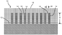
도 2는 본 발명의 실시 형태에 따른 평탄화 필름에 의한 표면 토포그래피의 평탄화를 예시하는, 도 1의 반도체 디바이스의 일부분의 개략 단면도이다.
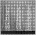
도 3은 고분자량 폴리(메틸 실세스퀴옥산) 수지로부터 형성된 평탄화 필름의 TEM 현미경 사진이다.
도 4는 본 발명의 실시 형태에 따라 형성된 평탄화 필름의 TEM 현미경 사진이다.
도 5는 본 발명의 실시 형태에 따라 형성된 다른 평탄화 필름의 TEM 현미경 사진이다.

Claims (10)
- 반도체 디바이스 표면을 평탄화(planarizing)하기 위한 조성물로서,
상기 조성물의 1 중량% 내지 40 중량% 범위의, 중량 평균 분자량이 500 Da 내지 5,000 Da인 폴리(메틸 실세스퀴옥산) 수지;
상기 조성물의 0.01 중량% 내지 0.20 중량% 범위의, 4차 암모늄 염과 아미노프로필트라이에톡시실란 염 중 적어도 하나; 및
상기 조성물의 잔부를 구성하는 적어도 하나의 용매
를 포함하는, 조성물. - 제1항에 있어서, 상기 적어도 하나의 용매는,
프로필렌 글리콜 메틸 에테르 아세테이트; 및
N-부틸 아세테이트
를 포함하는 용매 혼합물이며,
상기 프로필렌 글리콜 메틸 에테르 아세테이트 대 n-부틸 아세테이트의 중량비는 0.5:1 내지 2:1의 범위인, 조성물. - 제1항에 있어서, 상기 조성물의 0.05 중량% 내지 8 중량% 범위의 페닐 실세스퀴옥산을 추가로 포함하는, 조성물.
- 제1항에 있어서, 상기 폴리(메틸 실세스퀴옥산)은 중량 평균 분자량이 1,200 Da 내지 4,300 Da인, 조성물.
- 평탄화 조성물을 제조하기 위한 방법으로서,
중량 평균 분자량이 500 Da 내지 5,000 Da인 폴리(메틸 실세스퀴옥산) 수지를 제공하는 단계;
하나 이상의 용매들을 제공하는 단계;
상기 폴리(메틸 실세스퀴옥산) 수지를 상기 하나 이상의 용매들에 용해시켜 폴리(메틸 실세스퀴옥산) 용액을 형성하는 단계; 및
4차 암모늄 염과 아미노프로필트라이에톡시실란 염 중 적어도 하나를 상기 폴리(메틸 실세스퀴옥산) 용액에 용해시켜 상기 평탄화 조성물을 형성하는 단계
를 포함하는, 방법. - 제5항에 있어서, 상기 하나 이상의 용매들을 제공하는 단계는 프로필렌 글리콜 메틸 에테르 아세테이트 및 n-부틸 아세테이트를 함께 블렌딩하는 단계를 포함하며, 상기 프로필렌 글리콜 메틸 에테르 아세테이트 대 n-부틸 아세테이트의 중량비는 0.5:1 내지 2:1의 범위인, 방법.
- 제6항에 있어서, 상기 하나 이상의 용매들을 제공하는 단계는 고비점 용매를 상기 프로필렌 글리콜 메틸 에테르 아세테이트 및 상기 n-부틸 아세테이트와 함께 블렌딩하는 단계를 추가로 포함하며, 상기 고비점 용매는 비점이 154℃ 내지 274℃의 범위인, 방법.
- 제5항에 있어서,
페닐 실세스퀴옥산을 제공하는 단계;
상기 페닐 실세스퀴옥산을 용매에 용해시켜 페닐 실세스퀴옥산 용액을 형성하는 단계; 및
상기 페닐 실세스퀴옥산 용액을 상기 폴리(메틸 실세스퀴옥산) 용액과 블렌딩하여 상기 평탄화 조성물을 형성하는 단계
를 추가로 포함하는, 방법. - 반도체 디바이스를 위한 평탄화 필름으로서,
중량 평균 분자량이 500 Da 내지 5,000 Da인 폴리(메틸 실세스퀴옥산) 중합체 사슬들로 형성된 경화된 폴리(메틸 실세스퀴옥산)
을 포함하는, 평탄화 필름. - 제9항에 있어서, 4차 암모늄 염과 아미노프로필트라이에톡시실란 염 중 적어도 하나의 잔류물을 추가로 포함하는, 평탄화 필름.
Applications Claiming Priority (5)
| Application Number | Priority Date | Filing Date | Title |
|---|---|---|---|
| US201762448488P | 2017-01-20 | 2017-01-20 | |
| US62/448,488 | 2017-01-20 | ||
| US15/691,096 US10544330B2 (en) | 2017-01-20 | 2017-08-30 | Gap filling dielectric materials |
| US15/691,096 | 2017-08-30 | ||
| PCT/US2018/013745 WO2018136366A1 (en) | 2017-01-20 | 2018-01-15 | Gap filling dielectric materials |
Publications (2)
| Publication Number | Publication Date |
|---|---|
| KR20190103201A true KR20190103201A (ko) | 2019-09-04 |
| KR102554660B1 KR102554660B1 (ko) | 2023-07-13 |
Family
ID=62905749
Family Applications (1)
| Application Number | Title | Priority Date | Filing Date |
|---|---|---|---|
| KR1020197020559A Active KR102554660B1 (ko) | 2017-01-20 | 2018-01-15 | 간극 충전 유전체 재료 |
Country Status (7)
| Country | Link |
|---|---|
| US (1) | US10544330B2 (ko) |
| EP (1) | EP3571714A4 (ko) |
| JP (2) | JP2020507917A (ko) |
| KR (1) | KR102554660B1 (ko) |
| CN (1) | CN110192272A (ko) |
| TW (1) | TWI756340B (ko) |
| WO (1) | WO2018136366A1 (ko) |
Families Citing this family (4)
| Publication number | Priority date | Publication date | Assignee | Title |
|---|---|---|---|---|
| CN109233294B (zh) * | 2018-08-28 | 2020-04-24 | 淮阴工学院 | 有机硅介微孔超低介电薄膜及其制备方法 |
| JP2022550283A (ja) * | 2019-09-20 | 2022-12-01 | スリーエム イノベイティブ プロパティズ カンパニー | 低波面誤差光学フィルタフィルム |
| MX2022006254A (es) | 2019-12-05 | 2022-06-22 | Dow Global Technologies Llc | Composiciones de recubrimiento resistentes a la intemperie y duraderas. |
| US11499014B2 (en) | 2019-12-31 | 2022-11-15 | L'Air Liquide, Société Anonyme pour l'Etude et l'Exploitation des Procédés Georges Claude | Cureable formulations for forming low-k dielectric silicon-containing films using polycarbosilazane |
Citations (7)
| Publication number | Priority date | Publication date | Assignee | Title |
|---|---|---|---|---|
| EP0447611A2 (en) * | 1990-03-15 | 1991-09-25 | International Business Machines Corporation | Planarizing silsesquioxane copolymer coating |
| US20010051447A1 (en) * | 2000-05-16 | 2001-12-13 | Tatsuya Usami | Semiconductor device, semiconductor wafer, and methods of producing the same device and wafer |
| KR20020035594A (ko) * | 1999-09-09 | 2002-05-11 | 크리스 로저 에이치 | 집적회로 평탄화 장치 및 방법 |
| US20050089790A1 (en) * | 2003-09-02 | 2005-04-28 | Samsung Electronics Co., Ltd. | Photoresist composition for a spinless coater and method of forming a photoresist pattern using the same |
| US20110171447A1 (en) * | 2004-08-03 | 2011-07-14 | Ahila Krishnamoorthy | Compositions, layers and films for optoelectronic devices, methods of production and uses thereof |
| US20130209754A1 (en) * | 2012-02-09 | 2013-08-15 | Az Electronic Materials Usa Corp. | Low dielectric photoimageable compositions and electronic devices made therefrom |
| JP2015017195A (ja) * | 2013-07-11 | 2015-01-29 | 日産化学工業株式会社 | 固体撮像素子用リフロー型高屈折率膜形成組成物 |
Family Cites Families (28)
| Publication number | Priority date | Publication date | Assignee | Title |
|---|---|---|---|---|
| US5472488A (en) | 1990-09-14 | 1995-12-05 | Hyundai Electronics America | Coating solution for forming glassy layers |
| JPH07135212A (ja) | 1993-11-11 | 1995-05-23 | Showa Denko Kk | 半導体用絶縁膜または平坦化膜 |
| JP2893243B2 (ja) | 1994-11-25 | 1999-05-17 | 昭和電工株式会社 | 半導体絶縁膜用及び平坦化膜用組成物並びにその膜の形成方法 |
| JP3417464B2 (ja) * | 1998-06-24 | 2003-06-16 | 東京応化工業株式会社 | 平坦化膜形成用塗布液 |
| US6420441B1 (en) | 1999-10-01 | 2002-07-16 | Shipley Company, L.L.C. | Porous materials |
| US6815371B2 (en) | 2000-06-08 | 2004-11-09 | Honeywell International Inc. | Edge bead removal for spin-on materials containing low volatility solvents using carbon dioxide cleaning |
| US6685983B2 (en) | 2001-03-14 | 2004-02-03 | International Business Machines Corporation | Defect-free dielectric coatings and preparation thereof using polymeric nitrogenous porogens |
| US7005390B2 (en) | 2002-10-09 | 2006-02-28 | Intel Corporation | Replenishment of surface carbon and surface passivation of low-k porous silicon-based dielectric materials |
| JP3668222B2 (ja) | 2002-11-07 | 2005-07-06 | 株式会社東芝 | 半導体装置の製造方法 |
| JP4409515B2 (ja) | 2003-04-09 | 2010-02-03 | エルジー・ケム・リミテッド | 絶縁膜形成用コーティング組成物、その組成物を使用した低誘電絶縁膜の製造方法、その組成物より製造される半導体素子用低誘電絶縁膜およびその絶縁膜からなる半導体素子 |
| US7622399B2 (en) | 2003-09-23 | 2009-11-24 | Silecs Oy | Method of forming low-k dielectrics using a rapid curing process |
| US8101015B2 (en) | 2003-10-07 | 2012-01-24 | Honeywell International Inc. | Coatings and hard mask compositions for integrated circuit applications methods of production and uses thereof |
| US7553769B2 (en) | 2003-10-10 | 2009-06-30 | Tokyo Electron Limited | Method for treating a dielectric film |
| JP4564735B2 (ja) | 2003-10-22 | 2010-10-20 | 旭硝子株式会社 | 研磨スラリーおよび半導体集積回路の製造方法 |
| US8053159B2 (en) | 2003-11-18 | 2011-11-08 | Honeywell International Inc. | Antireflective coatings for via fill and photolithography applications and methods of preparation thereof |
| KR100621541B1 (ko) | 2004-02-06 | 2006-09-14 | 삼성전자주식회사 | 듀얼다마신 배선 형성방법 및 듀얼다마신 공정에서 보호막제거용 식각액 |
| US20050196974A1 (en) | 2004-03-02 | 2005-09-08 | Weigel Scott J. | Compositions for preparing low dielectric materials containing solvents |
| KR20060039628A (ko) | 2004-11-03 | 2006-05-09 | 삼성코닝 주식회사 | 용매확산이 억제된 저유전 다공성 박막 |
| KR101067596B1 (ko) | 2004-12-01 | 2011-09-27 | 삼성코닝정밀소재 주식회사 | 저유전 다공성 박막의 제조방법 |
| WO2006134206A2 (en) | 2005-06-13 | 2006-12-21 | Silecs Oy | Functionalized silane monomers with bridging hydrocarbon group and siloxane polymers of the same |
| JP2008033016A (ja) | 2006-07-28 | 2008-02-14 | Tokyo Ohka Kogyo Co Ltd | 多層レジスト用ポジ型レジスト組成物及びこれを用いたパターン形成方法 |
| CN101517487B (zh) | 2006-09-25 | 2012-08-08 | 日立化成工业株式会社 | 放射线敏感性组合物、二氧化硅系覆膜的形成方法、二氧化硅系覆膜、具有二氧化硅系覆膜的装置和部件以及绝缘膜用感光剂 |
| JP5863266B2 (ja) | 2011-04-12 | 2016-02-16 | メルクパフォーマンスマテリアルズIp合同会社 | シロキサン樹脂含有塗布組成物 |
| JP6007576B2 (ja) * | 2012-05-09 | 2016-10-12 | 日立化成株式会社 | 半導体装置の製造方法 |
| JP2014198699A (ja) * | 2013-03-29 | 2014-10-23 | 山本化成株式会社 | アントラキノン系化合物、及び光硬化性樹脂組成物 |
| US9738765B2 (en) | 2015-02-19 | 2017-08-22 | International Business Machines Corporation | Hybrid topographical and chemical pre-patterns for directed self-assembly of block copolymers |
| DE102015104439B4 (de) * | 2015-03-24 | 2019-02-21 | Bayerische Motoren Werke Aktiengesellschaft | Elektrochromes Element mit verbesserter Elektrolytschicht, Verfahren zu dessen Herstellung, Fahrzeugverglasung sowie Fahrzeug |
| JP2016188940A (ja) * | 2015-03-30 | 2016-11-04 | Jnc株式会社 | ポジ型感光性組成物 |
-
2017
- 2017-08-30 US US15/691,096 patent/US10544330B2/en active Active
-
2018
- 2018-01-15 EP EP18741757.1A patent/EP3571714A4/en not_active Withdrawn
- 2018-01-15 CN CN201880006635.9A patent/CN110192272A/zh active Pending
- 2018-01-15 WO PCT/US2018/013745 patent/WO2018136366A1/en not_active Ceased
- 2018-01-15 KR KR1020197020559A patent/KR102554660B1/ko active Active
- 2018-01-15 JP JP2019538227A patent/JP2020507917A/ja not_active Ceased
- 2018-01-18 TW TW107101809A patent/TWI756340B/zh active
-
2022
- 2022-02-25 JP JP2022027584A patent/JP7289950B2/ja active Active
Patent Citations (7)
| Publication number | Priority date | Publication date | Assignee | Title |
|---|---|---|---|---|
| EP0447611A2 (en) * | 1990-03-15 | 1991-09-25 | International Business Machines Corporation | Planarizing silsesquioxane copolymer coating |
| KR20020035594A (ko) * | 1999-09-09 | 2002-05-11 | 크리스 로저 에이치 | 집적회로 평탄화 장치 및 방법 |
| US20010051447A1 (en) * | 2000-05-16 | 2001-12-13 | Tatsuya Usami | Semiconductor device, semiconductor wafer, and methods of producing the same device and wafer |
| US20050089790A1 (en) * | 2003-09-02 | 2005-04-28 | Samsung Electronics Co., Ltd. | Photoresist composition for a spinless coater and method of forming a photoresist pattern using the same |
| US20110171447A1 (en) * | 2004-08-03 | 2011-07-14 | Ahila Krishnamoorthy | Compositions, layers and films for optoelectronic devices, methods of production and uses thereof |
| US20130209754A1 (en) * | 2012-02-09 | 2013-08-15 | Az Electronic Materials Usa Corp. | Low dielectric photoimageable compositions and electronic devices made therefrom |
| JP2015017195A (ja) * | 2013-07-11 | 2015-01-29 | 日産化学工業株式会社 | 固体撮像素子用リフロー型高屈折率膜形成組成物 |
Also Published As
| Publication number | Publication date |
|---|---|
| CN110192272A (zh) | 2019-08-30 |
| JP2022068349A (ja) | 2022-05-09 |
| JP2020507917A (ja) | 2020-03-12 |
| JP7289950B2 (ja) | 2023-06-12 |
| EP3571714A4 (en) | 2020-11-11 |
| KR102554660B1 (ko) | 2023-07-13 |
| EP3571714A1 (en) | 2019-11-27 |
| US20180208796A1 (en) | 2018-07-26 |
| US10544330B2 (en) | 2020-01-28 |
| WO2018136366A1 (en) | 2018-07-26 |
| TW201831580A (zh) | 2018-09-01 |
| TWI756340B (zh) | 2022-03-01 |
Similar Documents
| Publication | Publication Date | Title |
|---|---|---|
| JP7289950B2 (ja) | 間隙充填誘電材料 | |
| US6780499B2 (en) | Ordered two-phase dielectric film, and semiconductor device containing the same | |
| Xu et al. | Dielectric property and microstructure of a porous polymer material with ultralow dielectric constant | |
| US8541301B2 (en) | Reduction of pore fill material dewetting | |
| JP7053139B2 (ja) | 重合体、有機膜組成物、およびパターン形成方法 | |
| KR100760405B1 (ko) | 중합체 분해로부터 획득가능한 저 유전성 나노-다공성 물질 | |
| JP6573876B2 (ja) | 空隙形成用組成物、その組成物を用いて形成された空隙を具備した半導体装置、およびその組成物を用いた半導体装置の製造方法 | |
| KR20170040271A (ko) | 희생막용 조성물, 및 그 제조 방법, 및 그 조성물을 사용하여 형성된 공극을 구비한 반도체 장치, 및 그 조성물을 사용한 반도체 장치의 제조 방법 | |
| US6852648B2 (en) | Semiconductor device having a low dielectric constant dielectric material and process for its manufacture | |
| WO2005105894A2 (en) | SILOXANE EPOXY POLYMERS FOR LOW-κ DIELECTRIC APPLICATIONS | |
| TWI573844B (zh) | 塡隙方法 | |
| KR102723969B1 (ko) | 내균열성 폴리실록산 유전체 평탄화 조성물, 방법 및 필름 | |
| KR20190075581A (ko) | 유기막 조성물 및 패턴 형성 방법 | |
| US7910223B2 (en) | Planarization films for advanced microelectronic applications and devices and methods of production thereof | |
| KR102092798B1 (ko) | 유기막 제조 방법 및 패턴형성방법 | |
| US20160189822A1 (en) | Conductive Film and Method for Preparing the Same | |
| JP2006002125A (ja) | カルボシラン系ポリマーを含んでなる被膜形成用組成物、および該組成物から得られた被膜 | |
| KR20220142945A (ko) | 기판 세정용 조성물, 그를 이용하는 기판의 세정 방법 및 그를 이용하는 반도체 장치의 제조 방법 | |
| TW202336062A (zh) | 厚膜形成組成物及使用其製造固化膜的方法 | |
| CN117801313A (zh) | 嵌段共聚物共混导向自组装方法及系统 | |
| Takei et al. | Development of Developer-Soluble Gap Fill Materials for Planarization in Via-First Dual Damascene Process | |
| KR20190081973A (ko) | 화합물, 유기막 조성물 및 패턴 형성 방법 |
Legal Events
| Date | Code | Title | Description |
|---|---|---|---|
| PA0105 | International application |
St.27 status event code: A-0-1-A10-A15-nap-PA0105 |
|
| E13-X000 | Pre-grant limitation requested |
St.27 status event code: A-2-3-E10-E13-lim-X000 |
|
| P11-X000 | Amendment of application requested |
St.27 status event code: A-2-2-P10-P11-nap-X000 |
|
| P13-X000 | Application amended |
St.27 status event code: A-2-2-P10-P13-nap-X000 |
|
| P11-X000 | Amendment of application requested |
St.27 status event code: A-2-2-P10-P11-nap-X000 |
|
| P13-X000 | Application amended |
St.27 status event code: A-2-2-P10-P13-nap-X000 |
|
| R15-X000 | Change to inventor requested |
St.27 status event code: A-3-3-R10-R15-oth-X000 |
|
| R16-X000 | Change to inventor recorded |
St.27 status event code: A-3-3-R10-R16-oth-X000 |
|
| R17-X000 | Change to representative recorded |
St.27 status event code: A-3-3-R10-R17-oth-X000 |
|
| PG1501 | Laying open of application |
St.27 status event code: A-1-1-Q10-Q12-nap-PG1501 |
|
| R18-X000 | Changes to party contact information recorded |
St.27 status event code: A-3-3-R10-R18-oth-X000 |
|
| A201 | Request for examination | ||
| PA0201 | Request for examination |
St.27 status event code: A-1-2-D10-D11-exm-PA0201 |
|
| R18-X000 | Changes to party contact information recorded |
St.27 status event code: A-3-3-R10-R18-oth-X000 |
|
| E902 | Notification of reason for refusal | ||
| PE0902 | Notice of grounds for rejection |
St.27 status event code: A-1-2-D10-D21-exm-PE0902 |
|
| P11-X000 | Amendment of application requested |
St.27 status event code: A-2-2-P10-P11-nap-X000 |
|
| P13-X000 | Application amended |
St.27 status event code: A-2-2-P10-P13-nap-X000 |
|
| E701 | Decision to grant or registration of patent right | ||
| PE0701 | Decision of registration |
St.27 status event code: A-1-2-D10-D22-exm-PE0701 |
|
| PR0701 | Registration of establishment |
St.27 status event code: A-2-4-F10-F11-exm-PR0701 |
|
| PR1002 | Payment of registration fee |
St.27 status event code: A-2-2-U10-U12-oth-PR1002 Fee payment year number: 1 |
|
| PG1601 | Publication of registration |
St.27 status event code: A-4-4-Q10-Q13-nap-PG1601 |
|
| P22-X000 | Classification modified |
St.27 status event code: A-4-4-P10-P22-nap-X000 |