KR20200039867A - 유기 발광 표시 장치 - Google Patents
유기 발광 표시 장치 Download PDFInfo
- Publication number
- KR20200039867A KR20200039867A KR1020180118769A KR20180118769A KR20200039867A KR 20200039867 A KR20200039867 A KR 20200039867A KR 1020180118769 A KR1020180118769 A KR 1020180118769A KR 20180118769 A KR20180118769 A KR 20180118769A KR 20200039867 A KR20200039867 A KR 20200039867A
- Authority
- KR
- South Korea
- Prior art keywords
- layer
- electrode
- light emitting
- organic light
- semiconductor layer
- Prior art date
- Legal status (The legal status is an assumption and is not a legal conclusion. Google has not performed a legal analysis and makes no representation as to the accuracy of the status listed.)
- Ceased
Links
Images


Classifications
-
- H—ELECTRICITY
- H10—SEMICONDUCTOR DEVICES; ELECTRIC SOLID-STATE DEVICES NOT OTHERWISE PROVIDED FOR
- H10D—INORGANIC ELECTRIC SEMICONDUCTOR DEVICES
- H10D86/00—Integrated devices formed in or on insulating or conducting substrates, e.g. formed in silicon-on-insulator [SOI] substrates or on stainless steel or glass substrates
- H10D86/40—Integrated devices formed in or on insulating or conducting substrates, e.g. formed in silicon-on-insulator [SOI] substrates or on stainless steel or glass substrates characterised by multiple TFTs
- H10D86/421—Integrated devices formed in or on insulating or conducting substrates, e.g. formed in silicon-on-insulator [SOI] substrates or on stainless steel or glass substrates characterised by multiple TFTs having a particular composition, shape or crystalline structure of the active layer
- H10D86/423—Integrated devices formed in or on insulating or conducting substrates, e.g. formed in silicon-on-insulator [SOI] substrates or on stainless steel or glass substrates characterised by multiple TFTs having a particular composition, shape or crystalline structure of the active layer comprising semiconductor materials not belonging to the Group IV, e.g. InGaZnO
-
- H01L27/3262—
-
- H—ELECTRICITY
- H10—SEMICONDUCTOR DEVICES; ELECTRIC SOLID-STATE DEVICES NOT OTHERWISE PROVIDED FOR
- H10K—ORGANIC ELECTRIC SOLID-STATE DEVICES
- H10K59/00—Integrated devices, or assemblies of multiple devices, comprising at least one organic light-emitting element covered by group H10K50/00
- H10K59/10—OLED displays
- H10K59/12—Active-matrix OLED [AMOLED] displays
- H10K59/121—Active-matrix OLED [AMOLED] displays characterised by the geometry or disposition of pixel elements
- H10K59/1213—Active-matrix OLED [AMOLED] displays characterised by the geometry or disposition of pixel elements the pixel elements being TFTs
-
- H01L27/3276—
-
- H01L29/786—
-
- H01L51/5237—
-
- H—ELECTRICITY
- H10—SEMICONDUCTOR DEVICES; ELECTRIC SOLID-STATE DEVICES NOT OTHERWISE PROVIDED FOR
- H10K—ORGANIC ELECTRIC SOLID-STATE DEVICES
- H10K50/00—Organic light-emitting devices
- H10K50/80—Constructional details
- H10K50/84—Passivation; Containers; Encapsulations
- H10K50/844—Encapsulations
-
- H—ELECTRICITY
- H10—SEMICONDUCTOR DEVICES; ELECTRIC SOLID-STATE DEVICES NOT OTHERWISE PROVIDED FOR
- H10K—ORGANIC ELECTRIC SOLID-STATE DEVICES
- H10K59/00—Integrated devices, or assemblies of multiple devices, comprising at least one organic light-emitting element covered by group H10K50/00
- H10K59/10—OLED displays
- H10K59/12—Active-matrix OLED [AMOLED] displays
- H10K59/121—Active-matrix OLED [AMOLED] displays characterised by the geometry or disposition of pixel elements
- H10K59/1216—Active-matrix OLED [AMOLED] displays characterised by the geometry or disposition of pixel elements the pixel elements being capacitors
-
- H—ELECTRICITY
- H10—SEMICONDUCTOR DEVICES; ELECTRIC SOLID-STATE DEVICES NOT OTHERWISE PROVIDED FOR
- H10K—ORGANIC ELECTRIC SOLID-STATE DEVICES
- H10K59/00—Integrated devices, or assemblies of multiple devices, comprising at least one organic light-emitting element covered by group H10K50/00
- H10K59/10—OLED displays
- H10K59/12—Active-matrix OLED [AMOLED] displays
- H10K59/123—Connection of the pixel electrodes to the thin film transistors [TFT]
-
- H—ELECTRICITY
- H10—SEMICONDUCTOR DEVICES; ELECTRIC SOLID-STATE DEVICES NOT OTHERWISE PROVIDED FOR
- H10K—ORGANIC ELECTRIC SOLID-STATE DEVICES
- H10K59/00—Integrated devices, or assemblies of multiple devices, comprising at least one organic light-emitting element covered by group H10K50/00
- H10K59/10—OLED displays
- H10K59/12—Active-matrix OLED [AMOLED] displays
- H10K59/124—Insulating layers formed between TFT elements and OLED elements
-
- H—ELECTRICITY
- H10—SEMICONDUCTOR DEVICES; ELECTRIC SOLID-STATE DEVICES NOT OTHERWISE PROVIDED FOR
- H10K—ORGANIC ELECTRIC SOLID-STATE DEVICES
- H10K59/00—Integrated devices, or assemblies of multiple devices, comprising at least one organic light-emitting element covered by group H10K50/00
- H10K59/10—OLED displays
- H10K59/12—Active-matrix OLED [AMOLED] displays
- H10K59/126—Shielding, e.g. light-blocking means over the TFTs
-
- H—ELECTRICITY
- H10—SEMICONDUCTOR DEVICES; ELECTRIC SOLID-STATE DEVICES NOT OTHERWISE PROVIDED FOR
- H10K—ORGANIC ELECTRIC SOLID-STATE DEVICES
- H10K59/00—Integrated devices, or assemblies of multiple devices, comprising at least one organic light-emitting element covered by group H10K50/00
- H10K59/10—OLED displays
- H10K59/12—Active-matrix OLED [AMOLED] displays
- H10K59/131—Interconnections, e.g. wiring lines or terminals
- H10K59/1315—Interconnections, e.g. wiring lines or terminals comprising structures specially adapted for lowering the resistance
-
- H—ELECTRICITY
- H10—SEMICONDUCTOR DEVICES; ELECTRIC SOLID-STATE DEVICES NOT OTHERWISE PROVIDED FOR
- H10K—ORGANIC ELECTRIC SOLID-STATE DEVICES
- H10K59/00—Integrated devices, or assemblies of multiple devices, comprising at least one organic light-emitting element covered by group H10K50/00
- H10K59/80—Constructional details
- H10K59/87—Passivation; Containers; Encapsulations
- H10K59/873—Encapsulations
-
- H—ELECTRICITY
- H10—SEMICONDUCTOR DEVICES; ELECTRIC SOLID-STATE DEVICES NOT OTHERWISE PROVIDED FOR
- H10D—INORGANIC ELECTRIC SEMICONDUCTOR DEVICES
- H10D30/00—Field-effect transistors [FET]
- H10D30/60—Insulated-gate field-effect transistors [IGFET]
- H10D30/67—Thin-film transistors [TFT]
- H10D30/6704—Thin-film transistors [TFT] having supplementary regions or layers in the thin films or in the insulated bulk substrates for controlling properties of the device
- H10D30/6723—Thin-film transistors [TFT] having supplementary regions or layers in the thin films or in the insulated bulk substrates for controlling properties of the device having light shields
-
- H—ELECTRICITY
- H10—SEMICONDUCTOR DEVICES; ELECTRIC SOLID-STATE DEVICES NOT OTHERWISE PROVIDED FOR
- H10D—INORGANIC ELECTRIC SEMICONDUCTOR DEVICES
- H10D30/00—Field-effect transistors [FET]
- H10D30/60—Insulated-gate field-effect transistors [IGFET]
- H10D30/67—Thin-film transistors [TFT]
- H10D30/6729—Thin-film transistors [TFT] characterised by the electrodes
- H10D30/673—Thin-film transistors [TFT] characterised by the electrodes characterised by the shapes, relative sizes or dispositions of the gate electrodes
- H10D30/6731—Top-gate only TFTs
-
- H—ELECTRICITY
- H10—SEMICONDUCTOR DEVICES; ELECTRIC SOLID-STATE DEVICES NOT OTHERWISE PROVIDED FOR
- H10D—INORGANIC ELECTRIC SEMICONDUCTOR DEVICES
- H10D30/00—Field-effect transistors [FET]
- H10D30/60—Insulated-gate field-effect transistors [IGFET]
- H10D30/67—Thin-film transistors [TFT]
- H10D30/674—Thin-film transistors [TFT] characterised by the active materials
- H10D30/6741—Group IV materials, e.g. germanium or silicon carbide
- H10D30/6743—Silicon
- H10D30/6745—Polycrystalline or microcrystalline silicon
-
- H—ELECTRICITY
- H10—SEMICONDUCTOR DEVICES; ELECTRIC SOLID-STATE DEVICES NOT OTHERWISE PROVIDED FOR
- H10D—INORGANIC ELECTRIC SEMICONDUCTOR DEVICES
- H10D30/00—Field-effect transistors [FET]
- H10D30/60—Insulated-gate field-effect transistors [IGFET]
- H10D30/67—Thin-film transistors [TFT]
- H10D30/674—Thin-film transistors [TFT] characterised by the active materials
- H10D30/6755—Oxide semiconductors, e.g. zinc oxide, copper aluminium oxide or cadmium stannate
-
- H—ELECTRICITY
- H10—SEMICONDUCTOR DEVICES; ELECTRIC SOLID-STATE DEVICES NOT OTHERWISE PROVIDED FOR
- H10D—INORGANIC ELECTRIC SEMICONDUCTOR DEVICES
- H10D86/00—Integrated devices formed in or on insulating or conducting substrates, e.g. formed in silicon-on-insulator [SOI] substrates or on stainless steel or glass substrates
- H10D86/40—Integrated devices formed in or on insulating or conducting substrates, e.g. formed in silicon-on-insulator [SOI] substrates or on stainless steel or glass substrates characterised by multiple TFTs
- H10D86/441—Interconnections, e.g. scanning lines
-
- H—ELECTRICITY
- H10—SEMICONDUCTOR DEVICES; ELECTRIC SOLID-STATE DEVICES NOT OTHERWISE PROVIDED FOR
- H10D—INORGANIC ELECTRIC SEMICONDUCTOR DEVICES
- H10D86/00—Integrated devices formed in or on insulating or conducting substrates, e.g. formed in silicon-on-insulator [SOI] substrates or on stainless steel or glass substrates
- H10D86/40—Integrated devices formed in or on insulating or conducting substrates, e.g. formed in silicon-on-insulator [SOI] substrates or on stainless steel or glass substrates characterised by multiple TFTs
- H10D86/481—Integrated devices formed in or on insulating or conducting substrates, e.g. formed in silicon-on-insulator [SOI] substrates or on stainless steel or glass substrates characterised by multiple TFTs integrated with passive devices, e.g. auxiliary capacitors
-
- H—ELECTRICITY
- H10—SEMICONDUCTOR DEVICES; ELECTRIC SOLID-STATE DEVICES NOT OTHERWISE PROVIDED FOR
- H10D—INORGANIC ELECTRIC SEMICONDUCTOR DEVICES
- H10D86/00—Integrated devices formed in or on insulating or conducting substrates, e.g. formed in silicon-on-insulator [SOI] substrates or on stainless steel or glass substrates
- H10D86/40—Integrated devices formed in or on insulating or conducting substrates, e.g. formed in silicon-on-insulator [SOI] substrates or on stainless steel or glass substrates characterised by multiple TFTs
- H10D86/60—Integrated devices formed in or on insulating or conducting substrates, e.g. formed in silicon-on-insulator [SOI] substrates or on stainless steel or glass substrates characterised by multiple TFTs wherein the TFTs are in active matrices
Landscapes
- Engineering & Computer Science (AREA)
- Microelectronics & Electronic Packaging (AREA)
- Physics & Mathematics (AREA)
- Geometry (AREA)
- Optics & Photonics (AREA)
- Electroluminescent Light Sources (AREA)
- Devices For Indicating Variable Information By Combining Individual Elements (AREA)
Abstract
Description
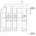
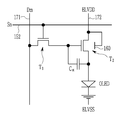
도 2는 일 실시예에 따른 유기 발광 표시 장치의 한 화소의 등가 회로도이다.
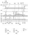
도 3은 일 실시예에 따른 유기 발광 표시 장치의 단면도이다.
도 4는 비교예와 일 실시예에 따른 유기 발광 표시 장치의 순간 잔상 지속 시간을 나타내는 그래프이다.
도 5는 다른 일 실시예에 따른 유기 발광 표시 장치의 한 화소의 등가 회로도이다.
도 6은 다른 일 실시예에 따른 유기 발광 표시 장치의 단면도이다.
도 7은 다른 일 실시예에 따른 유기 발광 표시 장치의 단면도이다.
123, 223: 제2 게이트 절연막 124, 224: 제3 게이트 절연막
136a, 236a: 제1 반도체층 136b, 236b: 제2 반도체층
155a, 255a: 제1 게이트 전극 155b, 265: 제2 게이트 전극
160, 260: 차단층 191: 화소 전극
270: 공통 전극 370: 유기 발광층
Claims (20)
- 기판,
상기 기판 위에 위치하는 제1 버퍼층,
상기 제1 버퍼층 위에 위치하는 제1 반도체층,
상기 제1 반도체층 위에 위치하는 제1 게이트 절연막,
상기 제1 게이트 절연막 위에 위치하는 제1 게이트 전극과 차단층,
상기 제1 게이트 전극 위에 위치하는 제2 버퍼층,
상기 제2 버퍼층 위에 위치하는 제2 반도체층,
상기 제2 반도체층 위에 위치하는 제2 게이트 절연막, 및
상기 제2 게이트 절연막 위에 위치하는 제2 게이트 전극을 포함하는 유기 발광 표시 장치. - 제1항에서,
상기 차단층은 상기 제2 반도체층과 중첩하는 유기 발광 표시 장치. - 제2항에서,
상기 차단층은 상기 제1 게이트 전극과 동일한 층에 위치하는 유기 발광 표시 장치. - 제3항에서,
구동 전압을 전달하는 구동 전압선을 더 포함하고,
상기 차단층은 상기 구동 전압선과 연결되어 상기 구동 전압을 인가 받는 유기 발광 표시 장치. - 제4항에서,
상기 제1 반도체층은,
상기 제1 게이트 전극과 중첩하는 제1 채널 영역, 및
상기 제1 채널 영역의 양 옆에 위치하는 제1 소스 영역과 제1 드레인 영역을 포함하고,
상기 제2 반도체층은,
상기 제2 게이트 전극과 중첩하는 제2 채널 영역, 및
상기 제2 채널 영역의 양 옆에 위치하는 제2 소스 영역과 제2 드레인 영역을 포함하는 유기 발광 표시 장치. - 제5항에서,
상기 차단층은 상기 제2 채널 영역과 중첩하는 유기 발광 표시 장치. - 제6항에서,
상기 제2 게이트 전극 위에 위치하는 제3 게이트 절연막, 및
상기 제3 게이트 절연막 위에 위치하고, 상기 제2 게이트 전극인 제1 유지 전극과 중첩하는 제2 유지 전극을 포함하는 유기 발광 표시 장치. - 제7항에서,
상기 제1 소스 영역 및 상기 제1 드레인 영역과 각각 연결되는 제1 소스 전극과 제1 드레인 전극, 및
상기 제2 소스 영역 및 상기 제2 드레인 영역과 각각 연결되는 제2 소스 전극과 제2 드레인 전극을 포함하고,
상기 제2 유지 전극은 상기 제2 드레인 전극과 연결되는 유기 발광 표시 장치. - 제8항에서,
상기 제2 유지 전극 위에 위치하는 화소 전극,
상기 화소 전극 위에 위치하는 유기 발광층, 및
상기 유기 발광층 위에 위치하는 공통 전극을 포함하고,
상기 제2 드레인 전극은 상기 화소 전극과 연결되는 유기 발광 표시 장치. - 제9항에서,
상기 공통 전극 위에 위치하는 봉지층을 더 포함하는 유기 발광 표시 장치. - 제7항에서,
상기 제1 소스 영역 및 상기 제1 드레인 영역과 각각 연결되는 제1 소스 전극과 제1 드레인 전극, 및
상기 제2 소스 영역 및 상기 제2 드레인 영역과 각각 연결되는 제2 소스 전극과 제2 드레인 전극을 포함하고,
상기 제2 유지 전극은 상기 구동 전압선과 연결되는 유기 발광 표시 장치. - 제11항에서,
상기 제1 반도체층과 상기 제2 반도체층 중 어느 하나는 산화물 반도체이고, 다른 하나는 다결정 규소를 포함하는 유기 발광 표시 장치. - 기판,
상기 기판 위에 위치하는 제1 트랜지스터,
상기 제1 트랜지스터 위에 위치하는 제2 트랜지스터, 및
상기 제2 트랜지스터의 아래에 위치하는 차단층을 포함하고,
상기 제1 트랜지스터는,
상기 기판 위에 위치하는 제1 반도체층, 및
상기 제1 반도체층 위에 위치하는 제1 게이트 전극을 포함하고,
상기 차단층은 상기 제1 반도체층 위에 위치하는 유기 발광 표시 장치. - 제13항에서,
상기 제1 트랜지스터와 상기 제2 트랜지스터 사이에 위치하는 버퍼층을 포함하고,
상기 제2 트랜지스터는,
상기 버퍼층 위에 위치하는 제2 반도체층, 및
상기 제2 반도체층 위에 위치하는 제2 게이트 전극을 포함하는 유기 발광 표시 장치. - 제14항에서,
상기 제2 반도체층은,
상기 제2 게이트 전극과 중첩하는 채널 영역, 및
상기 채널 영역의 양 옆에 위치하는 소스 영역과 드레인 영역을 포함하고,
상기 차단층은 상기 채널 영역과 중첩하는 유기 발광 표시 장치. - 제15항에서,
구동 전압을 전달하는 구동 전압선을 더 포함하고,
상기 차단층은 상기 구동 전압선에 연결되어 상기 구동 전압을 인가 받는 유기 발광 표시 장치. - 제16항에서,
상기 차단층은 상기 제1 게이트 전극과 동일한 층에 위치하는 유기 발광 표시 장치. - 제16항에서,
상기 제1 트랜지스터는 상기 제1 게이트 전극 위에 위치하고 상기 제1 게이트 전극과 중첩하는 제3 게이트 전극을 포함하고,
상기 차단층은 상기 제3 게이트 전극과 동일한 층에 위치하는 유기 발광 표시 장치. - 제18항에서,
상기 차단층은 상기 제2 반도체층의 상기 소스 영역과 상기 드레인 영역과도 중첩하는 유기 발광 표시 장치. - 제19항에서,
상기 제1 반도체층과 상기 제2 반도체층 중 어느 하나는 산화물 반도체이고, 다른 하나는 다결정 규소를 포함하는 유기 발광 표시 장치.
Priority Applications (7)
| Application Number | Priority Date | Filing Date | Title |
|---|---|---|---|
| KR1020180118769A KR20200039867A (ko) | 2018-10-05 | 2018-10-05 | 유기 발광 표시 장치 |
| CN201910940709.2A CN111009557B (zh) | 2018-10-05 | 2019-09-30 | 有机发光二极管显示器 |
| CN202510379267.4A CN120358888A (zh) | 2018-10-05 | 2019-09-30 | 有机发光二极管显示器 |
| US16/591,966 US11257886B2 (en) | 2018-10-05 | 2019-10-03 | Organic light emitting diode display |
| US17/572,913 US11856818B2 (en) | 2018-10-05 | 2022-01-11 | Organic light emitting diode display |
| US18/505,778 US20240081099A1 (en) | 2018-10-05 | 2023-11-09 | Organic light emitting diode display |
| KR1020240097313A KR20240119031A (ko) | 2018-10-05 | 2024-07-23 | 유기 발광 표시 장치 |
Applications Claiming Priority (1)
| Application Number | Priority Date | Filing Date | Title |
|---|---|---|---|
| KR1020180118769A KR20200039867A (ko) | 2018-10-05 | 2018-10-05 | 유기 발광 표시 장치 |
Related Child Applications (1)
| Application Number | Title | Priority Date | Filing Date |
|---|---|---|---|
| KR1020240097313A Division KR20240119031A (ko) | 2018-10-05 | 2024-07-23 | 유기 발광 표시 장치 |
Publications (1)
| Publication Number | Publication Date |
|---|---|
| KR20200039867A true KR20200039867A (ko) | 2020-04-17 |
Family
ID=70052440
Family Applications (2)
| Application Number | Title | Priority Date | Filing Date |
|---|---|---|---|
| KR1020180118769A Ceased KR20200039867A (ko) | 2018-10-05 | 2018-10-05 | 유기 발광 표시 장치 |
| KR1020240097313A Pending KR20240119031A (ko) | 2018-10-05 | 2024-07-23 | 유기 발광 표시 장치 |
Family Applications After (1)
| Application Number | Title | Priority Date | Filing Date |
|---|---|---|---|
| KR1020240097313A Pending KR20240119031A (ko) | 2018-10-05 | 2024-07-23 | 유기 발광 표시 장치 |
Country Status (3)
| Country | Link |
|---|---|
| US (3) | US11257886B2 (ko) |
| KR (2) | KR20200039867A (ko) |
| CN (2) | CN111009557B (ko) |
Cited By (2)
| Publication number | Priority date | Publication date | Assignee | Title |
|---|---|---|---|---|
| JP2022105315A (ja) * | 2020-12-31 | 2022-07-13 | エルジー ディスプレイ カンパニー リミテッド | 重畳した画素駆動部を含む表示装置 |
| US12133431B2 (en) | 2020-12-30 | 2024-10-29 | Samsung Display Co., Ltd. | Display apparatus |
Families Citing this family (18)
| Publication number | Priority date | Publication date | Assignee | Title |
|---|---|---|---|---|
| US10586495B2 (en) * | 2016-07-22 | 2020-03-10 | Semiconductor Energy Laboratory Co., Ltd. | Display device and electronic device |
| KR102741523B1 (ko) * | 2018-10-24 | 2024-12-11 | 삼성디스플레이 주식회사 | 유기 발광 표시 장치 |
| KR102925657B1 (ko) * | 2020-11-09 | 2026-02-09 | 엘지디스플레이 주식회사 | 발광 표시 장치 |
| US12336386B2 (en) | 2020-12-21 | 2025-06-17 | Boe Technology Group Co., Ltd. | Display substrate and manufacturing method thereof, and display device |
| KR20220091697A (ko) * | 2020-12-23 | 2022-07-01 | 삼성디스플레이 주식회사 | 표시 장치 및 그 리페어 방법 |
| KR20220092009A (ko) * | 2020-12-24 | 2022-07-01 | 엘지디스플레이 주식회사 | 기판 홀을 포함하는 표시장치 |
| KR102837639B1 (ko) * | 2020-12-30 | 2025-07-22 | 엘지디스플레이 주식회사 | 유기 발광 표시 장치 |
| KR102888466B1 (ko) * | 2021-07-13 | 2025-11-20 | 엘지디스플레이 주식회사 | 발광 소자 및 구동 회로를 포함하는 디스플레이 장치 |
| TWI774532B (zh) * | 2021-08-24 | 2022-08-11 | 友達光電股份有限公司 | 半導體裝置 |
| EP4141859B1 (en) * | 2021-08-25 | 2025-08-06 | LG Display Co., Ltd. | Display device |
| KR102890848B1 (ko) | 2021-08-30 | 2025-11-24 | 엘지디스플레이 주식회사 | 유기 발광 표시 장치 |
| KR102934008B1 (ko) * | 2021-08-30 | 2026-03-04 | 엘지디스플레이 주식회사 | 산화물 반도체를 포함하는 디스플레이 장치 |
| KR102940621B1 (ko) * | 2021-11-02 | 2026-03-17 | 엘지디스플레이 주식회사 | 박막 트랜지스터 및 이를 포함하는 표시장치 |
| KR20230089119A (ko) * | 2021-12-13 | 2023-06-20 | 엘지디스플레이 주식회사 | 산화물 반도체를 포함하는 디스플레이 장치 |
| KR102877032B1 (ko) | 2021-12-13 | 2025-10-28 | 삼성디스플레이 주식회사 | 화소 및 이를 포함하는 표시 장치 |
| KR20230166546A (ko) * | 2022-05-31 | 2023-12-07 | 엘지디스플레이 주식회사 | 박막 트랜지스터 및 이를 포함하는 표시 장치 |
| JP7461988B2 (ja) * | 2022-06-22 | 2024-04-04 | シャープディスプレイテクノロジー株式会社 | アクティブマトリクス基板および表示装置 |
| KR20240054800A (ko) * | 2022-10-19 | 2024-04-26 | 엘지디스플레이 주식회사 | 표시 장치 |
Family Cites Families (25)
| Publication number | Priority date | Publication date | Assignee | Title |
|---|---|---|---|---|
| US7507998B2 (en) | 2006-09-29 | 2009-03-24 | Tpo Displays Corp. | System for displaying images and method for fabricating the same |
| JP5366517B2 (ja) | 2007-12-03 | 2013-12-11 | 株式会社半導体エネルギー研究所 | 半導体装置の作製方法 |
| KR20260036405A (ko) * | 2009-10-29 | 2026-03-16 | 가부시키가이샤 한도오따이 에네루기 켄큐쇼 | 반도체 장치 |
| JP2011146465A (ja) * | 2010-01-13 | 2011-07-28 | Fujitsu Semiconductor Ltd | 半導体装置およびその製造方法 |
| KR101842585B1 (ko) * | 2010-12-30 | 2018-03-28 | 삼성디스플레이 주식회사 | 유기 발광 표시 장치 |
| CN103022012B (zh) * | 2011-09-21 | 2017-03-01 | 株式会社半导体能源研究所 | 半导体存储装置 |
| JP5960000B2 (ja) * | 2012-09-05 | 2016-08-02 | ルネサスエレクトロニクス株式会社 | 半導体装置及び半導体装置の製造方法 |
| US9818765B2 (en) * | 2013-08-26 | 2017-11-14 | Apple Inc. | Displays with silicon and semiconducting oxide thin-film transistors |
| KR102227474B1 (ko) | 2013-11-05 | 2021-03-15 | 삼성디스플레이 주식회사 | 박막트랜지스터 어레이 기판, 유기발광표시장치 및 박막트랜지스터 어레이 기판의 제조 방법 |
| KR102124025B1 (ko) * | 2013-12-23 | 2020-06-17 | 엘지디스플레이 주식회사 | 유기발광다이오드 표시장치 및 그 제조방법 |
| KR102132181B1 (ko) | 2013-12-31 | 2020-07-10 | 엘지디스플레이 주식회사 | 유기 발광 디스플레이 장치와 이의 제조 방법 |
| KR102467574B1 (ko) | 2014-08-29 | 2022-11-18 | 엘지디스플레이 주식회사 | 박막 트랜지스터 기판 및 이를 이용한 표시장치 |
| CN105390504B (zh) | 2014-08-29 | 2019-02-01 | 乐金显示有限公司 | 薄膜晶体管基板及使用它的显示装置 |
| KR101631549B1 (ko) * | 2014-09-04 | 2016-06-20 | 엘지디스플레이 주식회사 | 유기발광 표시패널 및 이를 제조하는 방법 |
| KR102280265B1 (ko) * | 2014-10-06 | 2021-07-22 | 삼성디스플레이 주식회사 | 박막 트랜지스터 어레이 기판, 및 이를 포함하는 유기 발광 표시 장치 |
| JP6512833B2 (ja) | 2015-01-16 | 2019-05-15 | 株式会社ジャパンディスプレイ | 表示装置 |
| KR102322085B1 (ko) * | 2015-02-23 | 2021-11-04 | 삼성디스플레이 주식회사 | 액정 표시 장치 |
| KR102303602B1 (ko) * | 2015-09-14 | 2021-09-17 | 삼성디스플레이 주식회사 | 표시 장치 |
| KR102387791B1 (ko) | 2015-12-31 | 2022-04-15 | 엘지디스플레이 주식회사 | 유기전계 발광표시장치 및 그 제조방법 |
| JP6692645B2 (ja) * | 2016-01-15 | 2020-05-13 | 株式会社ジャパンディスプレイ | 半導体装置 |
| JP6725317B2 (ja) * | 2016-05-19 | 2020-07-15 | 株式会社ジャパンディスプレイ | 表示装置 |
| US9985082B2 (en) * | 2016-07-06 | 2018-05-29 | Lg Display Co., Ltd. | Organic light emitting display device comprising multi-type thin film transistor and method of manufacturing the same |
| KR102716282B1 (ko) * | 2016-09-12 | 2024-10-11 | 삼성디스플레이 주식회사 | 테스트부를 갖는 표시장치 |
| KR102541552B1 (ko) * | 2016-11-30 | 2023-06-07 | 엘지디스플레이 주식회사 | 트랜지스터 기판 및 이를 이용한 유기발광표시패널과 유기발광표시장치 |
| CN108242453B (zh) * | 2016-12-23 | 2020-07-28 | 京东方科技集团股份有限公司 | 一种oled显示面板及显示装置 |
-
2018
- 2018-10-05 KR KR1020180118769A patent/KR20200039867A/ko not_active Ceased
-
2019
- 2019-09-30 CN CN201910940709.2A patent/CN111009557B/zh active Active
- 2019-09-30 CN CN202510379267.4A patent/CN120358888A/zh active Pending
- 2019-10-03 US US16/591,966 patent/US11257886B2/en active Active
-
2022
- 2022-01-11 US US17/572,913 patent/US11856818B2/en active Active
-
2023
- 2023-11-09 US US18/505,778 patent/US20240081099A1/en active Pending
-
2024
- 2024-07-23 KR KR1020240097313A patent/KR20240119031A/ko active Pending
Cited By (4)
| Publication number | Priority date | Publication date | Assignee | Title |
|---|---|---|---|---|
| US12133431B2 (en) | 2020-12-30 | 2024-10-29 | Samsung Display Co., Ltd. | Display apparatus |
| JP2022105315A (ja) * | 2020-12-31 | 2022-07-13 | エルジー ディスプレイ カンパニー リミテッド | 重畳した画素駆動部を含む表示装置 |
| JP2023085362A (ja) * | 2020-12-31 | 2023-06-20 | エルジー ディスプレイ カンパニー リミテッド | 重畳した画素駆動部を含む表示装置 |
| US12089453B2 (en) | 2020-12-31 | 2024-09-10 | Lg Display Co., Ltd. | Display apparatus comprising overlapped pixel driving circuits |
Also Published As
| Publication number | Publication date |
|---|---|
| US11856818B2 (en) | 2023-12-26 |
| KR20240119031A (ko) | 2024-08-06 |
| CN111009557B (zh) | 2025-04-25 |
| US20240081099A1 (en) | 2024-03-07 |
| CN120358888A (zh) | 2025-07-22 |
| US20200111855A1 (en) | 2020-04-09 |
| US11257886B2 (en) | 2022-02-22 |
| US20220140038A1 (en) | 2022-05-05 |
| CN111009557A (zh) | 2020-04-14 |
Similar Documents
| Publication | Publication Date | Title |
|---|---|---|
| US11856818B2 (en) | Organic light emitting diode display | |
| US11538408B2 (en) | Organic light-emitting diode display | |
| KR102392673B1 (ko) | 유기 발광 표시 장치 | |
| US9941340B2 (en) | Organic light-emitting diode display including a shielding electrode with reduced crosstalk | |
| KR102372775B1 (ko) | 유기 발광 표시 장치 | |
| KR102017764B1 (ko) | 유기 발광 표시 장치 | |
| US8376802B2 (en) | Organic electroluminescent display device and manufacturing method thereof | |
| KR102362092B1 (ko) | 유기 발광 표시 장치 | |
| KR102469793B1 (ko) | 표시 장치 | |
| KR102351507B1 (ko) | 유기 발광 표시 장치 | |
| US11563067B2 (en) | Display device with improved aperture ratio and transmissivity | |
| KR20180133280A (ko) | 표시 장치 | |
| US9647051B2 (en) | Organic light emitting diode display and repairing method thereof | |
| US20250318344A1 (en) | Display device | |
| KR101378855B1 (ko) | 유기전계발광표시장치 및 이의 구동방법 | |
| US12089461B2 (en) | Display device | |
| KR101367000B1 (ko) | 유기전계발광표시장치 | |
| KR101411745B1 (ko) | 유기전계발광표시장치 및 이의 구동방법 | |
| KR101388303B1 (ko) | 유기전계발광표시장치와 이의 구동방법 |
Legal Events
| Date | Code | Title | Description |
|---|---|---|---|
| PA0109 | Patent application |
St.27 status event code: A-0-1-A10-A12-nap-PA0109 |
|
| R18-X000 | Changes to party contact information recorded |
St.27 status event code: A-3-3-R10-R18-oth-X000 |
|
| PG1501 | Laying open of application |
St.27 status event code: A-1-1-Q10-Q12-nap-PG1501 |
|
| A201 | Request for examination | ||
| PA0201 | Request for examination |
St.27 status event code: A-1-2-D10-D11-exm-PA0201 |
|
| P22-X000 | Classification modified |
St.27 status event code: A-2-2-P10-P22-nap-X000 |
|
| P22-X000 | Classification modified |
St.27 status event code: A-2-2-P10-P22-nap-X000 |
|
| D13-X000 | Search requested |
St.27 status event code: A-1-2-D10-D13-srh-X000 |
|
| D14-X000 | Search report completed |
St.27 status event code: A-1-2-D10-D14-srh-X000 |
|
| E902 | Notification of reason for refusal | ||
| PE0902 | Notice of grounds for rejection |
St.27 status event code: A-1-2-D10-D21-exm-PE0902 |
|
| E13-X000 | Pre-grant limitation requested |
St.27 status event code: A-2-3-E10-E13-lim-X000 |
|
| P11-X000 | Amendment of application requested |
St.27 status event code: A-2-2-P10-P11-nap-X000 |
|
| P13-X000 | Application amended |
St.27 status event code: A-2-2-P10-P13-nap-X000 |
|
| E601 | Decision to refuse application | ||
| PE0601 | Decision on rejection of patent |
St.27 status event code: N-2-6-B10-B15-exm-PE0601 |
|
| PA0107 | Divisional application |
St.27 status event code: A-0-1-A10-A18-div-PA0107 St.27 status event code: A-0-1-A10-A16-div-PA0107 |
|
| P22-X000 | Classification modified |
St.27 status event code: A-2-2-P10-P22-nap-X000 |
|
| P22-X000 | Classification modified |
St.27 status event code: A-2-2-P10-P22-nap-X000 |