KR20200074163A - 노광장치 및 물품의 제조방법 - Google Patents
노광장치 및 물품의 제조방법 Download PDFInfo
- Publication number
- KR20200074163A KR20200074163A KR1020207013921A KR20207013921A KR20200074163A KR 20200074163 A KR20200074163 A KR 20200074163A KR 1020207013921 A KR1020207013921 A KR 1020207013921A KR 20207013921 A KR20207013921 A KR 20207013921A KR 20200074163 A KR20200074163 A KR 20200074163A
- Authority
- KR
- South Korea
- Prior art keywords
- light
- substrate
- amount
- receiving element
- exposure
- Prior art date
- Legal status (The legal status is an assumption and is not a legal conclusion. Google has not performed a legal analysis and makes no representation as to the accuracy of the status listed.)
- Granted
Links
Images


Classifications
-
- G—PHYSICS
- G03—PHOTOGRAPHY; CINEMATOGRAPHY; ANALOGOUS TECHNIQUES USING WAVES OTHER THAN OPTICAL WAVES; ELECTROGRAPHY; HOLOGRAPHY
- G03F—PHOTOMECHANICAL PRODUCTION OF TEXTURED OR PATTERNED SURFACES, e.g. FOR PRINTING, FOR PROCESSING OF SEMICONDUCTOR DEVICES; MATERIALS THEREFOR; ORIGINALS THEREFOR; APPARATUS SPECIALLY ADAPTED THEREFOR
- G03F7/00—Photomechanical, e.g. photolithographic, production of textured or patterned surfaces, e.g. printing surfaces; Materials therefor, e.g. comprising photoresists; Apparatus specially adapted therefor
- G03F7/70—Microphotolithographic exposure; Apparatus therefor
- G03F7/70483—Information management; Active and passive control; Testing; Wafer monitoring, e.g. pattern monitoring
- G03F7/70605—Workpiece metrology
- G03F7/70616—Monitoring the printed patterns
- G03F7/70641—Focus
-
- G—PHYSICS
- G03—PHOTOGRAPHY; CINEMATOGRAPHY; ANALOGOUS TECHNIQUES USING WAVES OTHER THAN OPTICAL WAVES; ELECTROGRAPHY; HOLOGRAPHY
- G03F—PHOTOMECHANICAL PRODUCTION OF TEXTURED OR PATTERNED SURFACES, e.g. FOR PRINTING, FOR PROCESSING OF SEMICONDUCTOR DEVICES; MATERIALS THEREFOR; ORIGINALS THEREFOR; APPARATUS SPECIALLY ADAPTED THEREFOR
- G03F9/00—Registration or positioning of originals, masks, frames, photographic sheets or textured or patterned surfaces, e.g. automatically
- G03F9/70—Registration or positioning of originals, masks, frames, photographic sheets or textured or patterned surfaces, e.g. automatically for microlithography
- G03F9/7003—Alignment type or strategy, e.g. leveling, global alignment
- G03F9/7023—Aligning or positioning in direction perpendicular to substrate surface
- G03F9/7026—Focusing
-
- G—PHYSICS
- G03—PHOTOGRAPHY; CINEMATOGRAPHY; ANALOGOUS TECHNIQUES USING WAVES OTHER THAN OPTICAL WAVES; ELECTROGRAPHY; HOLOGRAPHY
- G03F—PHOTOMECHANICAL PRODUCTION OF TEXTURED OR PATTERNED SURFACES, e.g. FOR PRINTING, FOR PROCESSING OF SEMICONDUCTOR DEVICES; MATERIALS THEREFOR; ORIGINALS THEREFOR; APPARATUS SPECIALLY ADAPTED THEREFOR
- G03F7/00—Photomechanical, e.g. photolithographic, production of textured or patterned surfaces, e.g. printing surfaces; Materials therefor, e.g. comprising photoresists; Apparatus specially adapted therefor
- G03F7/70—Microphotolithographic exposure; Apparatus therefor
- G03F7/70058—Mask illumination systems
- G03F7/70091—Illumination settings, i.e. intensity distribution in the pupil plane or angular distribution in the field plane; On-axis or off-axis settings, e.g. annular, dipole or quadrupole settings; Partial coherence control, i.e. sigma or numerical aperture [NA]
-
- G—PHYSICS
- G02—OPTICS
- G02B—OPTICAL ELEMENTS, SYSTEMS OR APPARATUS
- G02B7/00—Mountings, adjusting means, or light-tight connections, for optical elements
- G02B7/28—Systems for automatic generation of focusing signals
- G02B7/30—Systems for automatic generation of focusing signals using parallactic triangle with a base line
- G02B7/32—Systems for automatic generation of focusing signals using parallactic triangle with a base line using active means, e.g. light emitter
-
- G—PHYSICS
- G02—OPTICS
- G02B—OPTICAL ELEMENTS, SYSTEMS OR APPARATUS
- G02B7/00—Mountings, adjusting means, or light-tight connections, for optical elements
- G02B7/28—Systems for automatic generation of focusing signals
- G02B7/40—Systems for automatic generation of focusing signals using time delay of the reflected waves, e.g. of ultrasonic waves
-
- G—PHYSICS
- G03—PHOTOGRAPHY; CINEMATOGRAPHY; ANALOGOUS TECHNIQUES USING WAVES OTHER THAN OPTICAL WAVES; ELECTROGRAPHY; HOLOGRAPHY
- G03F—PHOTOMECHANICAL PRODUCTION OF TEXTURED OR PATTERNED SURFACES, e.g. FOR PRINTING, FOR PROCESSING OF SEMICONDUCTOR DEVICES; MATERIALS THEREFOR; ORIGINALS THEREFOR; APPARATUS SPECIALLY ADAPTED THEREFOR
- G03F7/00—Photomechanical, e.g. photolithographic, production of textured or patterned surfaces, e.g. printing surfaces; Materials therefor, e.g. comprising photoresists; Apparatus specially adapted therefor
- G03F7/70—Microphotolithographic exposure; Apparatus therefor
- G03F7/70058—Mask illumination systems
- G03F7/70091—Illumination settings, i.e. intensity distribution in the pupil plane or angular distribution in the field plane; On-axis or off-axis settings, e.g. annular, dipole or quadrupole settings; Partial coherence control, i.e. sigma or numerical aperture [NA]
- G03F7/70116—Off-axis setting using a programmable means, e.g. liquid crystal display [LCD], digital micromirror device [DMD] or pupil facets
-
- G—PHYSICS
- G03—PHOTOGRAPHY; CINEMATOGRAPHY; ANALOGOUS TECHNIQUES USING WAVES OTHER THAN OPTICAL WAVES; ELECTROGRAPHY; HOLOGRAPHY
- G03F—PHOTOMECHANICAL PRODUCTION OF TEXTURED OR PATTERNED SURFACES, e.g. FOR PRINTING, FOR PROCESSING OF SEMICONDUCTOR DEVICES; MATERIALS THEREFOR; ORIGINALS THEREFOR; APPARATUS SPECIALLY ADAPTED THEREFOR
- G03F7/00—Photomechanical, e.g. photolithographic, production of textured or patterned surfaces, e.g. printing surfaces; Materials therefor, e.g. comprising photoresists; Apparatus specially adapted therefor
- G03F7/70—Microphotolithographic exposure; Apparatus therefor
- G03F7/70058—Mask illumination systems
- G03F7/702—Reflective illumination, i.e. reflective optical elements other than folding mirrors, e.g. extreme ultraviolet [EUV] illumination systems
-
- G—PHYSICS
- G03—PHOTOGRAPHY; CINEMATOGRAPHY; ANALOGOUS TECHNIQUES USING WAVES OTHER THAN OPTICAL WAVES; ELECTROGRAPHY; HOLOGRAPHY
- G03F—PHOTOMECHANICAL PRODUCTION OF TEXTURED OR PATTERNED SURFACES, e.g. FOR PRINTING, FOR PROCESSING OF SEMICONDUCTOR DEVICES; MATERIALS THEREFOR; ORIGINALS THEREFOR; APPARATUS SPECIALLY ADAPTED THEREFOR
- G03F7/00—Photomechanical, e.g. photolithographic, production of textured or patterned surfaces, e.g. printing surfaces; Materials therefor, e.g. comprising photoresists; Apparatus specially adapted therefor
- G03F7/70—Microphotolithographic exposure; Apparatus therefor
- G03F7/70216—Mask projection systems
- G03F7/70258—Projection system adjustments, e.g. adjustments during exposure or alignment during assembly of projection system
-
- G—PHYSICS
- G03—PHOTOGRAPHY; CINEMATOGRAPHY; ANALOGOUS TECHNIQUES USING WAVES OTHER THAN OPTICAL WAVES; ELECTROGRAPHY; HOLOGRAPHY
- G03F—PHOTOMECHANICAL PRODUCTION OF TEXTURED OR PATTERNED SURFACES, e.g. FOR PRINTING, FOR PROCESSING OF SEMICONDUCTOR DEVICES; MATERIALS THEREFOR; ORIGINALS THEREFOR; APPARATUS SPECIALLY ADAPTED THEREFOR
- G03F7/00—Photomechanical, e.g. photolithographic, production of textured or patterned surfaces, e.g. printing surfaces; Materials therefor, e.g. comprising photoresists; Apparatus specially adapted therefor
- G03F7/70—Microphotolithographic exposure; Apparatus therefor
- G03F7/70216—Mask projection systems
- G03F7/70283—Mask effects on the imaging process
- G03F7/70291—Addressable masks, e.g. spatial light modulators [SLMs], digital micro-mirror devices [DMDs] or liquid crystal display [LCD] patterning devices
-
- G—PHYSICS
- G03—PHOTOGRAPHY; CINEMATOGRAPHY; ANALOGOUS TECHNIQUES USING WAVES OTHER THAN OPTICAL WAVES; ELECTROGRAPHY; HOLOGRAPHY
- G03F—PHOTOMECHANICAL PRODUCTION OF TEXTURED OR PATTERNED SURFACES, e.g. FOR PRINTING, FOR PROCESSING OF SEMICONDUCTOR DEVICES; MATERIALS THEREFOR; ORIGINALS THEREFOR; APPARATUS SPECIALLY ADAPTED THEREFOR
- G03F7/00—Photomechanical, e.g. photolithographic, production of textured or patterned surfaces, e.g. printing surfaces; Materials therefor, e.g. comprising photoresists; Apparatus specially adapted therefor
- G03F7/70—Microphotolithographic exposure; Apparatus therefor
- G03F7/70216—Mask projection systems
- G03F7/70358—Scanning exposure, i.e. relative movement of patterned beam and workpiece during imaging
-
- G—PHYSICS
- G03—PHOTOGRAPHY; CINEMATOGRAPHY; ANALOGOUS TECHNIQUES USING WAVES OTHER THAN OPTICAL WAVES; ELECTROGRAPHY; HOLOGRAPHY
- G03F—PHOTOMECHANICAL PRODUCTION OF TEXTURED OR PATTERNED SURFACES, e.g. FOR PRINTING, FOR PROCESSING OF SEMICONDUCTOR DEVICES; MATERIALS THEREFOR; ORIGINALS THEREFOR; APPARATUS SPECIALLY ADAPTED THEREFOR
- G03F7/00—Photomechanical, e.g. photolithographic, production of textured or patterned surfaces, e.g. printing surfaces; Materials therefor, e.g. comprising photoresists; Apparatus specially adapted therefor
- G03F7/70—Microphotolithographic exposure; Apparatus therefor
- G03F7/708—Construction of apparatus, e.g. environment aspects, hygiene aspects or materials
- G03F7/7085—Detection arrangement, e.g. detectors of apparatus alignment possibly mounted on wafers, exposure dose, photo-cleaning flux, stray light, thermal load
-
- H01L21/027—
-
- H—ELECTRICITY
- H10—SEMICONDUCTOR DEVICES; ELECTRIC SOLID-STATE DEVICES NOT OTHERWISE PROVIDED FOR
- H10P—GENERIC PROCESSES OR APPARATUS FOR THE MANUFACTURE OR TREATMENT OF DEVICES COVERED BY CLASS H10
- H10P76/00—Manufacture or treatment of masks on semiconductor bodies, e.g. by lithography or photolithography
Landscapes
- Physics & Mathematics (AREA)
- General Physics & Mathematics (AREA)
- Optics & Photonics (AREA)
- Health & Medical Sciences (AREA)
- Engineering & Computer Science (AREA)
- Environmental & Geological Engineering (AREA)
- Epidemiology (AREA)
- Public Health (AREA)
- Exposure And Positioning Against Photoresist Photosensitive Materials (AREA)
- Exposure Of Semiconductors, Excluding Electron Or Ion Beam Exposure (AREA)
- Focusing (AREA)
- Automatic Focus Adjustment (AREA)
Abstract
Description
도2는 제2실시형태에 따른 광학계의 구성을 도시한 도면이다.
도3은 제3실시형태에 따른 광학계의 구성을 도시한 도면이다.
도4는 제4실시형태에 따른 광학계의 구성을 도시한 도면이다.
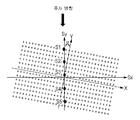
도5는 본 발명에 따른 기판 상의 주사 노광의 개요를 도시한 도면이다.
도6은 디포커스 량과 수광 소자의 검출 광량의 관계를 도시한 도면이다.
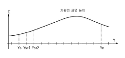
도7은 기판에 있어서의 표면 높이의 변동을 도시한 도면이다.
도8은 변형예 1에 관한 광학계의 구성을 도시한 도면이다.
도9는 변형예 1에 있어서의 디포커스 량과 수광 소자의 검출 광량의 관계를 도시한 도면이다.
도10은 변형예 2에 관한 광학계의 구성을 도시한 도면이다.
도11은 변형예 2에 있어서의 디포커스 량과 수광 소자의 검출 광량의 관계를 도시한 도면이다.
Claims (15)
- 기판에 패턴을 형성하기 위한 노광 광을 기판 위에 투영하는 투영 광학계와,
상기 기판에 있어서 반사된 빛을 통과시키기 위한 개구를 포함하는 차광부재와,
상기 기판에 있어서 반사된 후에 상기 개구를 통과한 광속을 수광하는 수광 소자와,
상기 수광 소자에 있어서 수광된 광량에 따라, 상기 노광 광의 집광 위치와 상기 기판의 위치 어긋남을 나타내는 디포커스 량을 변화시키는 포커스 제어를 행하는 것을 특징으로 하는 노광장치.
- 제 1항에 있어서,
상기 차광부재는, 상기 디포커스 량이 소정 량보다도 작은 초점맞춤 상태에 있어서 상기 기판과 광학적으로 공역의 면에 배치되어 있는 것을 특징으로 하는 노광장치.
- 제 1항 또는 제 2항에 있어서,
상기 제어부는, 상기 차광부재를 상기 투영 광학계의 광축 방향으로 이동시키는 것을 특징으로 하는 노광장치.
- 제 3항에 있어서,
상기 제어부는, 상기 수광 소자에 있어서 수광되는 광량이 증가하도록, 상기 차광부재를 이동시키는 것을 특징으로 하는 노광장치.
- 제 1항에 있어서,
상기 제어부는, 상기 투영 광학계의 광로에 배치된 광학부재를 상기 투영 광학계의 광축 방향으로 이동시키는 것을 특징으로 하는 노광장치.
- 제 5항에 있어서,
상기 제어부는, 상기 수광 소자에 있어서 수광되는 광량이 증가하도록, 상기 광학부재를 이동시키는 것을 특징으로 하는 노광장치.
- 제 1항에 있어서,
상기 기판에 있어서 반사된 빛을 더 반사하는 반사부재를 갖고,
상기 차광부재는, 상기 반사부재에 의해 반사된 광로 중에 배치되어 있는 것을 특징으로 하는 노광장치.
- 제 7항에 있어서,
상기 차광부재는, 상기 디포커스 량이 소정 량보다도 작은 초점맞춤 상태에 있어서 상기 기판과 광학적으로 공역의 면으로부터 어긋나게 배치되어 있는 것을 특징으로 하는 노광장치.
- 제 1항 내지 제 8항 중 어느 한 항에 있어서,
상기 차광부재는 금속으로 구성되는 것을 특징으로 하는 노광장치.
- 제 1항 내지 제 9항 중 어느 한 항에 있어서,
복수의 광 변조 소자를 포함하는 광 변조부와,
상기 광 변조부에 빛을 조사하는 조명 광학계를 더 갖고,
상기 광 변조부에 의해 반사된 빛이 상기 투영 광학계에 입사되는 것을 특징으로 하는 노광장치.
- 제 10항에 있어서,
상기 포커스 제어가 행해진 상태에서, 상기 조명 광학계에 의해 형성된 스폿 광을 상기 투영 광학계를 거쳐 상기 기판 위에 투영하는 노광 동작을 행하고,
상기 기판 위의 특정한 영역에 대하여 상기 노광 동작을 반복하는 것을 특징으로 하는 노광장치.
- 기판에 패턴을 형성하기 위한 노광 광을 기판 위에 투영하는 투영 광학계를 포함하는 노광장치로서,
상기 기판에 있어서 반사된 빛을 통과시키기 위한 개구를 포함하는 제1 차광부재와,
상기 기판에 있어서 반사된 후에 상기 제1 차광부재의 개구를 통과한 광속을 수광하는 제1 수광 소자와,
상기 기판에 있어서 반사된 빛을 통과시키기 위한 개구를 포함하는 제2 차광부재와,
상기 기판에 있어서 반사된 후에 상기 제2 차광부재의 개구를 통과한 광속을 수광하는 제2 수광 소자를 갖고,
상기 제1 차광부재는, 상기 노광 광의 집광 위치와 상기 기판의 위치 어긋남을 나타내는 디포커스 량이 소정 량보다도 작은 초점맞춤 상태에 있어서 상기 기판과 광학적으로 공역의 면으로부터 상기 제1 수광 소자측으로 어긋나게 배치되고,
상기 제2 차광부재는, 상기 초점맞춤 상태에 있어서 상기 기판과 광학적으로 공역의 면으로부터 상기 제2 수광 소자와는 반대측으로 어긋나게 배치되어 있는 것을 특징으로 하는 노광장치.
- 제 12항에 있어서,
상기 제1 수광 소자 및 상기 제2 수광 소자에 있어서 수광된 광량에 따라, 상기 디포커스 량을 변화시키는 포커스 제어를 행하는 것을 특징으로 하는 노광장치.
- 기판에 패턴을 형성하기 위한 노광 광을 기판 위에 투영하는 투영 광학계와, 상기 노광 광의 집광 위치를 변화시키는 광학부재를 포함하는 노광 유닛과,
상기 기판에 있어서 반사된 빛을 통과시키기 위한 개구를 포함하는 차광부재와, 상기 기판에 있어서 반사된 후에 상기 차광부재의 개구를 통과한 광속을 수광하는 수광 소자를 포함하는 광학 유닛을 갖는 노광장치로서,
상기 수광 소자에 있어서 수광된 광량에 따라, 상기 광학부재를 상기 투영 광학계의 광축 방향으로 이동시키는 것을 특징으로 하는 노광장치.
- 청구항 1 내지 14 중 어느 한 항에 기재된 노광장치를 사용해서 기판을 노광하는 공정과,
상기 공정에서 노광된 상기 기판을 현상하는 공정을 포함하는 것을 특징으로 하는 물품의 제조방법.
Applications Claiming Priority (5)
| Application Number | Priority Date | Filing Date | Title |
|---|---|---|---|
| JP2017205644 | 2017-10-24 | ||
| JPJP-P-2017-205644 | 2017-10-24 | ||
| JP2018146251A JP2019079030A (ja) | 2017-10-24 | 2018-08-02 | 露光装置および物品の製造方法 |
| JPJP-P-2018-146251 | 2018-08-02 | ||
| PCT/JP2018/038416 WO2019082726A1 (ja) | 2017-10-24 | 2018-10-16 | 露光装置および物品の製造方法 |
Publications (2)
| Publication Number | Publication Date |
|---|---|
| KR20200074163A true KR20200074163A (ko) | 2020-06-24 |
| KR102433510B1 KR102433510B1 (ko) | 2022-08-18 |
Family
ID=66626547
Family Applications (1)
| Application Number | Title | Priority Date | Filing Date |
|---|---|---|---|
| KR1020207013921A Active KR102433510B1 (ko) | 2017-10-24 | 2018-10-16 | 노광장치 및 물품의 제조방법 |
Country Status (4)
| Country | Link |
|---|---|
| US (1) | US10921717B2 (ko) |
| JP (1) | JP2019079030A (ko) |
| KR (1) | KR102433510B1 (ko) |
| CN (1) | CN111356955A (ko) |
Families Citing this family (2)
| Publication number | Priority date | Publication date | Assignee | Title |
|---|---|---|---|---|
| CN112394619A (zh) * | 2019-08-13 | 2021-02-23 | 苏州源卓光电科技有限公司 | 一种直写光刻机的曝光系统 |
| US12189137B2 (en) * | 2022-02-23 | 2025-01-07 | The Boeing Company | System and method for super-resolution imaging |
Citations (7)
| Publication number | Priority date | Publication date | Assignee | Title |
|---|---|---|---|---|
| US5117254A (en) * | 1988-05-13 | 1992-05-26 | Canon Kabushiki Kaisha | Projection exposure apparatus |
| JP2004062155A (ja) | 2002-06-07 | 2004-02-26 | Fuji Photo Film Co Ltd | 露光ヘッド及び露光装置 |
| JP2006060152A (ja) * | 2004-08-24 | 2006-03-02 | Nikon Corp | 光学特性測定装置、ステージ装置及び露光装置 |
| KR20090115685A (ko) * | 2008-05-01 | 2009-11-05 | 캐논 가부시끼가이샤 | 주사 노광 장치 및 디바이스 제조 방법 |
| JP2011002512A (ja) | 2009-06-16 | 2011-01-06 | Hitachi High-Technologies Corp | 露光装置、露光方法、及び表示用パネル基板の製造方法 |
| JP2013520819A (ja) * | 2010-02-23 | 2013-06-06 | エーエスエムエル ネザーランズ ビー.ブイ. | リソグラフィ装置及びデバイス製造方法 |
| JP2015012258A (ja) * | 2013-07-02 | 2015-01-19 | キヤノン株式会社 | 露光装置、露光方法、それらを用いたデバイスの製造方法 |
Family Cites Families (8)
| Publication number | Priority date | Publication date | Assignee | Title |
|---|---|---|---|---|
| US5117255A (en) * | 1990-09-19 | 1992-05-26 | Nikon Corporation | Projection exposure apparatus |
| JPH104053A (ja) * | 1996-06-13 | 1998-01-06 | Canon Inc | 面位置検出装置及びそれを用いたデバイスの製造方法 |
| US5969820A (en) | 1996-06-13 | 1999-10-19 | Canon Kabushiki Kaisha | Surface position detecting system and exposure apparatus using the same |
| JP4312535B2 (ja) * | 2003-08-06 | 2009-08-12 | シャープ株式会社 | パターン露光装置 |
| JP2007286243A (ja) * | 2006-04-14 | 2007-11-01 | Sumitomo Heavy Ind Ltd | 露光装置 |
| EP2048543B1 (en) * | 2007-10-09 | 2013-12-04 | ASML Netherlands B.V. | An optical focus sensor, an inspection apparatus and a lithographic apparatus |
| JP5842808B2 (ja) * | 2010-02-20 | 2016-01-13 | 株式会社ニコン | 瞳強度分布を調整する方法 |
| WO2013023876A1 (en) * | 2011-08-18 | 2013-02-21 | Asml Netherlands B.V. | Lithographic apparatus and device manufacturing method |
-
2018
- 2018-08-02 JP JP2018146251A patent/JP2019079030A/ja active Pending
- 2018-10-16 CN CN201880069270.4A patent/CN111356955A/zh active Pending
- 2018-10-16 KR KR1020207013921A patent/KR102433510B1/ko active Active
-
2020
- 2020-04-20 US US16/853,431 patent/US10921717B2/en active Active
Patent Citations (7)
| Publication number | Priority date | Publication date | Assignee | Title |
|---|---|---|---|---|
| US5117254A (en) * | 1988-05-13 | 1992-05-26 | Canon Kabushiki Kaisha | Projection exposure apparatus |
| JP2004062155A (ja) | 2002-06-07 | 2004-02-26 | Fuji Photo Film Co Ltd | 露光ヘッド及び露光装置 |
| JP2006060152A (ja) * | 2004-08-24 | 2006-03-02 | Nikon Corp | 光学特性測定装置、ステージ装置及び露光装置 |
| KR20090115685A (ko) * | 2008-05-01 | 2009-11-05 | 캐논 가부시끼가이샤 | 주사 노광 장치 및 디바이스 제조 방법 |
| JP2011002512A (ja) | 2009-06-16 | 2011-01-06 | Hitachi High-Technologies Corp | 露光装置、露光方法、及び表示用パネル基板の製造方法 |
| JP2013520819A (ja) * | 2010-02-23 | 2013-06-06 | エーエスエムエル ネザーランズ ビー.ブイ. | リソグラフィ装置及びデバイス製造方法 |
| JP2015012258A (ja) * | 2013-07-02 | 2015-01-19 | キヤノン株式会社 | 露光装置、露光方法、それらを用いたデバイスの製造方法 |
Also Published As
| Publication number | Publication date |
|---|---|
| KR102433510B1 (ko) | 2022-08-18 |
| JP2019079030A (ja) | 2019-05-23 |
| CN111356955A (zh) | 2020-06-30 |
| US20200249582A1 (en) | 2020-08-06 |
| US10921717B2 (en) | 2021-02-16 |
Similar Documents
| Publication | Publication Date | Title |
|---|---|---|
| KR101444981B1 (ko) | 노광 장치, 노광 방법 및 디바이스 제조 방법 | |
| JP4315455B2 (ja) | 露光装置及びデバイス製造方法 | |
| TWI693667B (zh) | 移動體之控制方法、曝光方法、元件製造方法、移動體裝置、及曝光裝置 | |
| KR20180138544A (ko) | 노광 장치 및 물품의 제조 방법 | |
| KR102222673B1 (ko) | 노광 장치 및 물품 제조 방법 | |
| JP6267530B2 (ja) | 露光装置、および物品の製造方法 | |
| JP5137879B2 (ja) | 露光装置及びデバイス製造方法 | |
| KR101660090B1 (ko) | 노광 방법, 노광 장치, 및 디바이스의 제조 방법 | |
| KR102433510B1 (ko) | 노광장치 및 물품의 제조방법 | |
| JP6327861B2 (ja) | リソグラフィ装置、リソグラフィ方法、および物品の製造方法 | |
| JP2009164355A (ja) | 走査露光装置およびデバイス製造方法 | |
| KR102433491B1 (ko) | 노광장치 및 물품의 제조방법 | |
| KR102756371B1 (ko) | 노광 장치 및 물품의 제조 방법 | |
| JP6436856B2 (ja) | 露光装置、露光方法、および物品の製造方法 | |
| US20100110400A1 (en) | Scanning exposure apparatus, control method therefor, and device manufacturing method | |
| WO2019082726A1 (ja) | 露光装置および物品の製造方法 | |
| US20260118775A1 (en) | Exposure apparatus, exposure method, and article manufacturing method | |
| WO2019082727A1 (ja) | 露光装置および物品の製造方法 | |
| JP2014143429A (ja) | 露光装置、露光方法及びデバイス製造方法 | |
| KR102519522B1 (ko) | 리소그래피 장치, 조명 장치 및 물품의 제조 방법 | |
| JP2008124308A (ja) | 露光方法及び露光装置、それを用いたデバイス製造方法 | |
| KR20240175295A (ko) | 노광 장치, 노광 방법 및 물품 제조 방법 | |
| JP6053316B2 (ja) | リソグラフィー装置、および、物品製造方法 | |
| JPH0875415A (ja) | アライメント装置 | |
| JP2011138887A (ja) | 露光装置 |
Legal Events
| Date | Code | Title | Description |
|---|---|---|---|
| A201 | Request for examination | ||
| E13-X000 | Pre-grant limitation requested |
St.27 status event code: A-2-3-E10-E13-lim-X000 |
|
| P11-X000 | Amendment of application requested |
St.27 status event code: A-2-2-P10-P11-nap-X000 |
|
| P13-X000 | Application amended |
St.27 status event code: A-2-2-P10-P13-nap-X000 |
|
| PA0105 | International application |
St.27 status event code: A-0-1-A10-A15-nap-PA0105 |
|
| PA0201 | Request for examination |
St.27 status event code: A-1-2-D10-D11-exm-PA0201 |
|
| PG1501 | Laying open of application |
St.27 status event code: A-1-1-Q10-Q12-nap-PG1501 |
|
| D13-X000 | Search requested |
St.27 status event code: A-1-2-D10-D13-srh-X000 |
|
| D14-X000 | Search report completed |
St.27 status event code: A-1-2-D10-D14-srh-X000 |
|
| E902 | Notification of reason for refusal | ||
| PE0902 | Notice of grounds for rejection |
St.27 status event code: A-1-2-D10-D21-exm-PE0902 |
|
| T11-X000 | Administrative time limit extension requested |
St.27 status event code: U-3-3-T10-T11-oth-X000 |
|
| T11-X000 | Administrative time limit extension requested |
St.27 status event code: U-3-3-T10-T11-oth-X000 |
|
| P11-X000 | Amendment of application requested |
St.27 status event code: A-2-2-P10-P11-nap-X000 |
|
| P13-X000 | Application amended |
St.27 status event code: A-2-2-P10-P13-nap-X000 |
|
| E701 | Decision to grant or registration of patent right | ||
| PE0701 | Decision of registration |
St.27 status event code: A-1-2-D10-D22-exm-PE0701 |
|
| GRNT | Written decision to grant | ||
| PR0701 | Registration of establishment |
St.27 status event code: A-2-4-F10-F11-exm-PR0701 |
|
| PR1002 | Payment of registration fee |
St.27 status event code: A-2-2-U10-U12-oth-PR1002 Fee payment year number: 1 |
|
| PG1601 | Publication of registration |
St.27 status event code: A-4-4-Q10-Q13-nap-PG1601 |
|
| PR1001 | Payment of annual fee |
St.27 status event code: A-4-4-U10-U11-oth-PR1001 Fee payment year number: 4 |
|
| U11 | Full renewal or maintenance fee paid |
Free format text: ST27 STATUS EVENT CODE: A-4-4-U10-U11-OTH-PR1001 (AS PROVIDED BY THE NATIONAL OFFICE) Year of fee payment: 4 |
|
| P22-X000 | Classification modified |
St.27 status event code: A-4-4-P10-P22-nap-X000 |