KR20200089549A - 비아홀이 형성된 태양전지의 제조 방법 - Google Patents
비아홀이 형성된 태양전지의 제조 방법 Download PDFInfo
- Publication number
- KR20200089549A KR20200089549A KR1020190006420A KR20190006420A KR20200089549A KR 20200089549 A KR20200089549 A KR 20200089549A KR 1020190006420 A KR1020190006420 A KR 1020190006420A KR 20190006420 A KR20190006420 A KR 20190006420A KR 20200089549 A KR20200089549 A KR 20200089549A
- Authority
- KR
- South Korea
- Prior art keywords
- solar cell
- forming
- layer
- manufacturing
- type silicon
- Prior art date
- Legal status (The legal status is an assumption and is not a legal conclusion. Google has not performed a legal analysis and makes no representation as to the accuracy of the status listed.)
- Ceased
Links
- 238000000034 method Methods 0.000 title claims abstract description 37
- 238000004519 manufacturing process Methods 0.000 title claims abstract description 25
- 229910021419 crystalline silicon Inorganic materials 0.000 title description 2
- 238000002161 passivation Methods 0.000 claims abstract description 33
- 239000004065 semiconductor Substances 0.000 claims abstract description 21
- 230000000149 penetrating effect Effects 0.000 claims abstract description 5
- XUIMIQQOPSSXEZ-UHFFFAOYSA-N Silicon Chemical compound [Si] XUIMIQQOPSSXEZ-UHFFFAOYSA-N 0.000 claims description 35
- 229910052710 silicon Inorganic materials 0.000 claims description 35
- 239000010703 silicon Substances 0.000 claims description 35
- 238000005553 drilling Methods 0.000 claims description 11
- 238000002834 transmittance Methods 0.000 claims description 11
- 238000000151 deposition Methods 0.000 claims description 6
- KWYUFKZDYYNOTN-UHFFFAOYSA-M Potassium hydroxide Chemical compound [OH-].[K+] KWYUFKZDYYNOTN-UHFFFAOYSA-M 0.000 claims description 3
- 229910004298 SiO 2 Inorganic materials 0.000 claims description 3
- XLYOFNOQVPJJNP-UHFFFAOYSA-N water Substances O XLYOFNOQVPJJNP-UHFFFAOYSA-N 0.000 claims description 3
- 238000010248 power generation Methods 0.000 description 5
- 239000003086 colorant Substances 0.000 description 4
- 239000000126 substance Substances 0.000 description 4
- 230000000694 effects Effects 0.000 description 3
- 238000005516 engineering process Methods 0.000 description 3
- 229910052581 Si3N4 Inorganic materials 0.000 description 2
- 230000005540 biological transmission Effects 0.000 description 2
- 239000004566 building material Substances 0.000 description 2
- 238000003486 chemical etching Methods 0.000 description 2
- 229910052751 metal Inorganic materials 0.000 description 2
- 239000002184 metal Substances 0.000 description 2
- 239000002086 nanomaterial Substances 0.000 description 2
- HQVNEWCFYHHQES-UHFFFAOYSA-N silicon nitride Chemical compound N12[Si]34N5[Si]62N3[Si]51N64 HQVNEWCFYHHQES-UHFFFAOYSA-N 0.000 description 2
- 229910018072 Al 2 O 3 Inorganic materials 0.000 description 1
- OAICVXFJPJFONN-UHFFFAOYSA-N Phosphorus Chemical compound [P] OAICVXFJPJFONN-UHFFFAOYSA-N 0.000 description 1
- 229910004205 SiNX Inorganic materials 0.000 description 1
- BQCADISMDOOEFD-UHFFFAOYSA-N Silver Chemical compound [Ag] BQCADISMDOOEFD-UHFFFAOYSA-N 0.000 description 1
- 229910052782 aluminium Inorganic materials 0.000 description 1
- XAGFODPZIPBFFR-UHFFFAOYSA-N aluminium Chemical compound [Al] XAGFODPZIPBFFR-UHFFFAOYSA-N 0.000 description 1
- 239000003245 coal Substances 0.000 description 1
- 238000010276 construction Methods 0.000 description 1
- 239000004035 construction material Substances 0.000 description 1
- 230000005611 electricity Effects 0.000 description 1
- 239000002803 fossil fuel Substances 0.000 description 1
- 238000012986 modification Methods 0.000 description 1
- 230000004048 modification Effects 0.000 description 1
- 239000003208 petroleum Substances 0.000 description 1
- 230000003334 potential effect Effects 0.000 description 1
- 230000006798 recombination Effects 0.000 description 1
- 238000005215 recombination Methods 0.000 description 1
- 238000002310 reflectometry Methods 0.000 description 1
- 239000005368 silicate glass Substances 0.000 description 1
- 229910052709 silver Inorganic materials 0.000 description 1
- 239000004332 silver Substances 0.000 description 1
- 230000003746 surface roughness Effects 0.000 description 1
- 239000010409 thin film Substances 0.000 description 1
Images


Classifications
-
- H01L31/047—
-
- H—ELECTRICITY
- H10—SEMICONDUCTOR DEVICES; ELECTRIC SOLID-STATE DEVICES NOT OTHERWISE PROVIDED FOR
- H10F—INORGANIC SEMICONDUCTOR DEVICES SENSITIVE TO INFRARED RADIATION, LIGHT, ELECTROMAGNETIC RADIATION OF SHORTER WAVELENGTH OR CORPUSCULAR RADIATION
- H10F19/00—Integrated devices, or assemblies of multiple devices, comprising at least one photovoltaic cell covered by group H10F10/00, e.g. photovoltaic modules
- H10F19/10—Integrated devices, or assemblies of multiple devices, comprising at least one photovoltaic cell covered by group H10F10/00, e.g. photovoltaic modules comprising photovoltaic cells in arrays in a single semiconductor substrate, the photovoltaic cells having vertical junctions or V-groove junctions
-
- H01L31/022425—
-
- H01L31/1868—
-
- H—ELECTRICITY
- H02—GENERATION; CONVERSION OR DISTRIBUTION OF ELECTRIC POWER
- H02S—GENERATION OF ELECTRIC POWER BY CONVERSION OF INFRARED RADIATION, VISIBLE LIGHT OR ULTRAVIOLET LIGHT, e.g. USING PHOTOVOLTAIC [PV] MODULES
- H02S20/00—Supporting structures for PV modules
- H02S20/20—Supporting structures directly fixed to an immovable object
- H02S20/22—Supporting structures directly fixed to an immovable object specially adapted for buildings
- H02S20/26—Building materials integrated with PV modules, e.g. façade elements
-
- H—ELECTRICITY
- H10—SEMICONDUCTOR DEVICES; ELECTRIC SOLID-STATE DEVICES NOT OTHERWISE PROVIDED FOR
- H10F—INORGANIC SEMICONDUCTOR DEVICES SENSITIVE TO INFRARED RADIATION, LIGHT, ELECTROMAGNETIC RADIATION OF SHORTER WAVELENGTH OR CORPUSCULAR RADIATION
- H10F71/00—Manufacture or treatment of devices covered by this subclass
- H10F71/129—Passivating
-
- H—ELECTRICITY
- H10—SEMICONDUCTOR DEVICES; ELECTRIC SOLID-STATE DEVICES NOT OTHERWISE PROVIDED FOR
- H10F—INORGANIC SEMICONDUCTOR DEVICES SENSITIVE TO INFRARED RADIATION, LIGHT, ELECTROMAGNETIC RADIATION OF SHORTER WAVELENGTH OR CORPUSCULAR RADIATION
- H10F77/00—Constructional details of devices covered by this subclass
- H10F77/20—Electrodes
- H10F77/206—Electrodes for devices having potential barriers
- H10F77/211—Electrodes for devices having potential barriers for photovoltaic cells
-
- Y—GENERAL TAGGING OF NEW TECHNOLOGICAL DEVELOPMENTS; GENERAL TAGGING OF CROSS-SECTIONAL TECHNOLOGIES SPANNING OVER SEVERAL SECTIONS OF THE IPC; TECHNICAL SUBJECTS COVERED BY FORMER USPC CROSS-REFERENCE ART COLLECTIONS [XRACs] AND DIGESTS
- Y02—TECHNOLOGIES OR APPLICATIONS FOR MITIGATION OR ADAPTATION AGAINST CLIMATE CHANGE
- Y02E—REDUCTION OF GREENHOUSE GAS [GHG] EMISSIONS, RELATED TO ENERGY GENERATION, TRANSMISSION OR DISTRIBUTION
- Y02E10/00—Energy generation through renewable energy sources
- Y02E10/50—Photovoltaic [PV] energy
-
- Y—GENERAL TAGGING OF NEW TECHNOLOGICAL DEVELOPMENTS; GENERAL TAGGING OF CROSS-SECTIONAL TECHNOLOGIES SPANNING OVER SEVERAL SECTIONS OF THE IPC; TECHNICAL SUBJECTS COVERED BY FORMER USPC CROSS-REFERENCE ART COLLECTIONS [XRACs] AND DIGESTS
- Y02—TECHNOLOGIES OR APPLICATIONS FOR MITIGATION OR ADAPTATION AGAINST CLIMATE CHANGE
- Y02P—CLIMATE CHANGE MITIGATION TECHNOLOGIES IN THE PRODUCTION OR PROCESSING OF GOODS
- Y02P70/00—Climate change mitigation technologies in the production process for final industrial or consumer products
- Y02P70/50—Manufacturing or production processes characterised by the final manufactured product
Landscapes
- Engineering & Computer Science (AREA)
- Architecture (AREA)
- Civil Engineering (AREA)
- Structural Engineering (AREA)
- Life Sciences & Earth Sciences (AREA)
- Sustainable Development (AREA)
- Sustainable Energy (AREA)
- Photovoltaic Devices (AREA)
Abstract
Description
도 2는 본 발명의 일 실시예에 따른 태양전지의 구조를 도시한 도면이다.
도 3은 본 발명의 일 실시예에 따른 옥사이드층에 의한 다양한 색상의 태양전지를 도시한 도면이다.
도 4는 본 발명의 일 실시예에 따른 비아홀의 형성 방법을 도시한다.
도 5는 본 발명의 일 실시예에 따른 비아홀이 형성된 태양전지를 도시한 도면이다.
201: N-형 실리콘층
203: P-형 실 리콘층
205: 상부 패시베이션층
207: 하부 패시베이션층
209: 하부 전극
211: 비아홀
Claims (10)
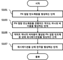
- PN 접합 반도체층을 형성하는 단계;
상기 PN 접합 반도체층을 관통하는 적어도 하나의 비아홀(via-hole)을 형성하는 단계;
상기 적어도 하나의 비아홀이 형성된 PN 접합 반도체층 상에 패시베이션층을 형성하는 단계; 및
상기 패시베이션층 상에 전극을 형성하는 단계;
를 포함하는,
태양전지의 제조 방법.
- 제1항에 있어서,
상기 전극을 형성하는 단계 이전에, 상기 패시베이션층 상에 옥사이드층을 형성하는 단계;
를 더 포함하는,
태양전지의 제조 방법.
- 제2항에 있어서,
상기 태양전지의 색상은, 상기 옥사이드층의 두께에 따라 조절되는,
태양전지의 제조 방법.
- 제2항에 있어서,
상기 옥사이드층은 SiO2 옥사이드층을 포함하는,
태양전지의 제조 방법.
- 제1항에 있어서,
상기 적어도 하나의 비아홀을 형성하는 단계는,
수산화칼륨(KOH) 용액이 담긴 수조에 상기 전극이 형성된 태양전지를 함침시키는 단계; 및
상기 태양전지가 함침된 상태에서 레이저 드릴링 공정을 수행하여 상기 적어도 하나의 비아홀을 형성하는 단계;
를 포함하는,
태양전지의 제조 방법.
- 제5항에 있어서,
상기 적어도 하나의 비아홀은, 상기 PN 접합 반도체층에 포함된 N-형 실리콘층과 P-형 실리콘층의 적층 구조를 수직으로 관통하는 방향으로 형성되는,
태양전지의 제조 방법.
- 제1항에 있어서,
상기 적어도 하나의 비아홀의 형태는, 상기 태양전지에 입사되는 태양광의 투과율을 결정하는,
태양전지의 제조 방법.
- 제7항에 있어서,
상기 적어도 하나의 비아홀의 형태는 타원형인,
태양전지의 제조 방법.
- 제1항에 있어서,
상기 PN 접합 반도체층을 형성하는 단계는,
P-형 실리콘층을 형성하는 단계; 및
상기 P-형 실리콘층 상부에 N-형 실리콘층을 적층하는 단계;
를 포함하는,
태양전지의 제조 방법.
- 제9항에 있어서,
상기 패시베이션층을 형성하는 단계는,
상기 N-형 실리콘층 상부에 상부 패시베이션층을 적층하는 단계; 및
상기 P-형 실리콘층 하부에 하부 패시베이션층을 적층하는 단계;
를 포함하는,
태양전지의 제조 방법.
Priority Applications (1)
| Application Number | Priority Date | Filing Date | Title |
|---|---|---|---|
| KR1020190006420A KR20200089549A (ko) | 2019-01-17 | 2019-01-17 | 비아홀이 형성된 태양전지의 제조 방법 |
Applications Claiming Priority (1)
| Application Number | Priority Date | Filing Date | Title |
|---|---|---|---|
| KR1020190006420A KR20200089549A (ko) | 2019-01-17 | 2019-01-17 | 비아홀이 형성된 태양전지의 제조 방법 |
Publications (1)
| Publication Number | Publication Date |
|---|---|
| KR20200089549A true KR20200089549A (ko) | 2020-07-27 |
Family
ID=71894039
Family Applications (1)
| Application Number | Title | Priority Date | Filing Date |
|---|---|---|---|
| KR1020190006420A Ceased KR20200089549A (ko) | 2019-01-17 | 2019-01-17 | 비아홀이 형성된 태양전지의 제조 방법 |
Country Status (1)
| Country | Link |
|---|---|
| KR (1) | KR20200089549A (ko) |
Citations (1)
| Publication number | Priority date | Publication date | Assignee | Title |
|---|---|---|---|---|
| KR101690678B1 (ko) | 2015-10-07 | 2016-12-28 | 문여진 | 태양광 발전 창호 |
-
2019
- 2019-01-17 KR KR1020190006420A patent/KR20200089549A/ko not_active Ceased
Patent Citations (1)
| Publication number | Priority date | Publication date | Assignee | Title |
|---|---|---|---|---|
| KR101690678B1 (ko) | 2015-10-07 | 2016-12-28 | 문여진 | 태양광 발전 창호 |
Similar Documents
| Publication | Publication Date | Title |
|---|---|---|
| US8889462B2 (en) | Photovoltaic solar cells | |
| CN102171838B (zh) | 太阳能电池及其制造方法 | |
| JP2010537423A (ja) | 異種接合シリコン太陽電池及びその製造方法 | |
| US20110139250A1 (en) | Bifacial solar cell | |
| CN105122463A (zh) | 使用体晶片的单片岛型背接触背结太阳能电池 | |
| KR101072543B1 (ko) | 태양 전지의 제조 방법 | |
| CN118658899A (zh) | 背接触太阳能电池、光伏组件及光伏系统 | |
| CN109585600A (zh) | 一种双面perc高效晶硅太阳能电池的制作方法 | |
| CN107946408A (zh) | 一种ibc太阳能电池的制备方法 | |
| KR20180020375A (ko) | 태양전지 패널 및 이를 구비한 창호 | |
| CN103187482A (zh) | 一种晶硅太阳能mwt电池的制造方法及其制造的电池 | |
| KR100964153B1 (ko) | 태양전지의 제조방법 및 그에 의해 제조되는 태양전지 | |
| CN222897500U (zh) | 背接触太阳能电池、光伏组件及光伏系统 | |
| KR101198438B1 (ko) | 양면 수광형 국부화 에미터 태양전지 및 그 제조 방법 | |
| Ho et al. | Rear-surface line-contact optimization using screen-print techniques on crystalline solar cells for industrial applications | |
| KR20200089549A (ko) | 비아홀이 형성된 태양전지의 제조 방법 | |
| WO2015046728A1 (ko) | 태양전지모듈 | |
| Rasheed et al. | Silicon-Based Technologies for Solar | |
| KR101181625B1 (ko) | 국부화 에미터 태양전지 및 그 제조 방법 | |
| KR101382047B1 (ko) | 태양전지의 선택적 에미터 형성방법 | |
| KR101251878B1 (ko) | 양면 수광형 태양전지 제조 방법 | |
| KR101114198B1 (ko) | 국부화 에미터 태양전지 및 그 제조 방법 | |
| CN206657812U (zh) | 太阳能电池 | |
| Abdul Rasheed et al. | Silicon-Based Technologies for Solar to Photovoltaic Conversion | |
| Ripon et al. | Efficiency enhancement of solar cell: Fusion of texturisation and back contact Emitter-Wrap-Through modeling |
Legal Events
| Date | Code | Title | Description |
|---|---|---|---|
| PA0109 | Patent application |
Patent event code: PA01091R01D Comment text: Patent Application Patent event date: 20190117 |
|
| PA0201 | Request for examination | ||
| E902 | Notification of reason for refusal | ||
| PE0902 | Notice of grounds for rejection |
Comment text: Notification of reason for refusal Patent event date: 20200716 Patent event code: PE09021S01D |
|
| PG1501 | Laying open of application | ||
| E601 | Decision to refuse application | ||
| PE0601 | Decision on rejection of patent |
Patent event date: 20201016 Comment text: Decision to Refuse Application Patent event code: PE06012S01D Patent event date: 20200716 Comment text: Notification of reason for refusal Patent event code: PE06011S01I |
|
| E601 | Decision to refuse application | ||
| E801 | Decision on dismissal of amendment | ||
| PE0601 | Decision on rejection of patent |
Patent event date: 20210115 Comment text: Decision to Refuse Application Patent event code: PE06012S01D Patent event date: 20200716 Comment text: Notification of reason for refusal Patent event code: PE06011S01I |
|
| PE0801 | Dismissal of amendment |
Patent event code: PE08012E01D Comment text: Decision on Dismissal of Amendment Patent event date: 20210115 Patent event code: PE08011R01I Comment text: Amendment to Specification, etc. Patent event date: 20201221 Patent event code: PE08011R01I Comment text: Amendment to Specification, etc. Patent event date: 20200916 |