KR20200092349A - 3-d ic응용 제품을 위한 레이저로 분리 가능한 접착 재료 - Google Patents
3-d ic응용 제품을 위한 레이저로 분리 가능한 접착 재료 Download PDFInfo
- Publication number
- KR20200092349A KR20200092349A KR1020207018152A KR20207018152A KR20200092349A KR 20200092349 A KR20200092349 A KR 20200092349A KR 1020207018152 A KR1020207018152 A KR 1020207018152A KR 20207018152 A KR20207018152 A KR 20207018152A KR 20200092349 A KR20200092349 A KR 20200092349A
- Authority
- KR
- South Korea
- Prior art keywords
- diglycidyl ether
- substrate
- layer
- ether
- adhesive layer
- Prior art date
- Legal status (The legal status is an assumption and is not a legal conclusion. Google has not performed a legal analysis and makes no representation as to the accuracy of the status listed.)
- Granted
Links
Images


Classifications
-
- C—CHEMISTRY; METALLURGY
- C08—ORGANIC MACROMOLECULAR COMPOUNDS; THEIR PREPARATION OR CHEMICAL WORKING-UP; COMPOSITIONS BASED THEREON
- C08L—COMPOSITIONS OF MACROMOLECULAR COMPOUNDS
- C08L71/00—Compositions of polyethers obtained by reactions forming an ether link in the main chain; Compositions of derivatives of such polymers
- C08L71/08—Polyethers derived from hydroxy compounds or from their metallic derivatives
- C08L71/10—Polyethers derived from hydroxy compounds or from their metallic derivatives from phenols
- C08L71/12—Polyphenylene oxides
-
- B—PERFORMING OPERATIONS; TRANSPORTING
- B32—LAYERED PRODUCTS
- B32B—LAYERED PRODUCTS, i.e. PRODUCTS BUILT-UP OF STRATA OF FLAT OR NON-FLAT, e.g. CELLULAR OR HONEYCOMB, FORM
- B32B7/00—Layered products characterised by the relation between layers; Layered products characterised by the relative orientation of features between layers, or by the relative values of a measurable parameter between layers, i.e. products comprising layers having different physical, chemical or physicochemical properties; Layered products characterised by the interconnection of layers
- B32B7/04—Interconnection of layers
- B32B7/06—Interconnection of layers permitting easy separation
-
- B—PERFORMING OPERATIONS; TRANSPORTING
- B32—LAYERED PRODUCTS
- B32B—LAYERED PRODUCTS, i.e. PRODUCTS BUILT-UP OF STRATA OF FLAT OR NON-FLAT, e.g. CELLULAR OR HONEYCOMB, FORM
- B32B27/00—Layered products comprising a layer of synthetic resin
- B32B27/18—Layered products comprising a layer of synthetic resin characterised by the use of special additives
- B32B27/20—Layered products comprising a layer of synthetic resin characterised by the use of special additives using fillers, pigments, thixotroping agents
-
- B—PERFORMING OPERATIONS; TRANSPORTING
- B32—LAYERED PRODUCTS
- B32B—LAYERED PRODUCTS, i.e. PRODUCTS BUILT-UP OF STRATA OF FLAT OR NON-FLAT, e.g. CELLULAR OR HONEYCOMB, FORM
- B32B27/00—Layered products comprising a layer of synthetic resin
- B32B27/28—Layered products comprising a layer of synthetic resin comprising synthetic resins not wholly covered by any one of the sub-groups B32B27/30 - B32B27/42
- B32B27/285—Layered products comprising a layer of synthetic resin comprising synthetic resins not wholly covered by any one of the sub-groups B32B27/30 - B32B27/42 comprising polyethers
-
- B—PERFORMING OPERATIONS; TRANSPORTING
- B32—LAYERED PRODUCTS
- B32B—LAYERED PRODUCTS, i.e. PRODUCTS BUILT-UP OF STRATA OF FLAT OR NON-FLAT, e.g. CELLULAR OR HONEYCOMB, FORM
- B32B27/00—Layered products comprising a layer of synthetic resin
- B32B27/38—Layered products comprising a layer of synthetic resin comprising epoxy resins
-
- B—PERFORMING OPERATIONS; TRANSPORTING
- B32—LAYERED PRODUCTS
- B32B—LAYERED PRODUCTS, i.e. PRODUCTS BUILT-UP OF STRATA OF FLAT OR NON-FLAT, e.g. CELLULAR OR HONEYCOMB, FORM
- B32B7/00—Layered products characterised by the relation between layers; Layered products characterised by the relative orientation of features between layers, or by the relative values of a measurable parameter between layers, i.e. products comprising layers having different physical, chemical or physicochemical properties; Layered products characterised by the interconnection of layers
- B32B7/04—Interconnection of layers
- B32B7/12—Interconnection of layers using interposed adhesives or interposed materials with bonding properties
-
- C—CHEMISTRY; METALLURGY
- C08—ORGANIC MACROMOLECULAR COMPOUNDS; THEIR PREPARATION OR CHEMICAL WORKING-UP; COMPOSITIONS BASED THEREON
- C08K—Use of inorganic or non-macromolecular organic substances as compounding ingredients
- C08K3/00—Use of inorganic substances as compounding ingredients
-
- C—CHEMISTRY; METALLURGY
- C09—DYES; PAINTS; POLISHES; NATURAL RESINS; ADHESIVES; COMPOSITIONS NOT OTHERWISE PROVIDED FOR; APPLICATIONS OF MATERIALS NOT OTHERWISE PROVIDED FOR
- C09J—ADHESIVES; NON-MECHANICAL ASPECTS OF ADHESIVE PROCESSES IN GENERAL; ADHESIVE PROCESSES NOT PROVIDED FOR ELSEWHERE; USE OF MATERIALS AS ADHESIVES
- C09J11/00—Features of adhesives not provided for in group C09J9/00, e.g. additives
- C09J11/02—Non-macromolecular additives
- C09J11/06—Non-macromolecular additives organic
-
- C—CHEMISTRY; METALLURGY
- C09—DYES; PAINTS; POLISHES; NATURAL RESINS; ADHESIVES; COMPOSITIONS NOT OTHERWISE PROVIDED FOR; APPLICATIONS OF MATERIALS NOT OTHERWISE PROVIDED FOR
- C09J—ADHESIVES; NON-MECHANICAL ASPECTS OF ADHESIVE PROCESSES IN GENERAL; ADHESIVE PROCESSES NOT PROVIDED FOR ELSEWHERE; USE OF MATERIALS AS ADHESIVES
- C09J171/00—Adhesives based on polyethers obtained by reactions forming an ether link in the main chain; Adhesives based on derivatives of such polymers
- C09J171/08—Polyethers derived from hydroxy compounds or from their metallic derivatives
-
- C—CHEMISTRY; METALLURGY
- C09—DYES; PAINTS; POLISHES; NATURAL RESINS; ADHESIVES; COMPOSITIONS NOT OTHERWISE PROVIDED FOR; APPLICATIONS OF MATERIALS NOT OTHERWISE PROVIDED FOR
- C09J—ADHESIVES; NON-MECHANICAL ASPECTS OF ADHESIVE PROCESSES IN GENERAL; ADHESIVE PROCESSES NOT PROVIDED FOR ELSEWHERE; USE OF MATERIALS AS ADHESIVES
- C09J5/00—Adhesive processes in general; Adhesive processes not provided for elsewhere, e.g. relating to primers
- C09J5/04—Adhesive processes in general; Adhesive processes not provided for elsewhere, e.g. relating to primers involving separate application of adhesive ingredients to the different surfaces to be joined
-
- H01L21/185—
-
- H01L21/268—
-
- H01L24/27—
-
- H—ELECTRICITY
- H10—SEMICONDUCTOR DEVICES; ELECTRIC SOLID-STATE DEVICES NOT OTHERWISE PROVIDED FOR
- H10P—GENERIC PROCESSES OR APPARATUS FOR THE MANUFACTURE OR TREATMENT OF DEVICES COVERED BY CLASS H10
- H10P10/00—Bonding of wafers, substrates or parts of devices
- H10P10/12—Bonding of semiconductor wafers or semiconductor substrates to semiconductor wafers or semiconductor substrates
-
- H—ELECTRICITY
- H10—SEMICONDUCTOR DEVICES; ELECTRIC SOLID-STATE DEVICES NOT OTHERWISE PROVIDED FOR
- H10P—GENERIC PROCESSES OR APPARATUS FOR THE MANUFACTURE OR TREATMENT OF DEVICES COVERED BY CLASS H10
- H10P34/00—Irradiation with electromagnetic or particle radiation of wafers, substrates or parts of devices
- H10P34/40—Irradiation with electromagnetic or particle radiation of wafers, substrates or parts of devices with high-energy radiation
- H10P34/42—Irradiation with electromagnetic or particle radiation of wafers, substrates or parts of devices with high-energy radiation with electromagnetic radiation, e.g. laser annealing
-
- H—ELECTRICITY
- H10—SEMICONDUCTOR DEVICES; ELECTRIC SOLID-STATE DEVICES NOT OTHERWISE PROVIDED FOR
- H10P—GENERIC PROCESSES OR APPARATUS FOR THE MANUFACTURE OR TREATMENT OF DEVICES COVERED BY CLASS H10
- H10P72/00—Handling or holding of wafers, substrates or devices during manufacture or treatment thereof
- H10P72/70—Handling or holding of wafers, substrates or devices during manufacture or treatment thereof for supporting or gripping
- H10P72/74—Handling or holding of wafers, substrates or devices during manufacture or treatment thereof for supporting or gripping using temporarily an auxiliary support
-
- H—ELECTRICITY
- H10—SEMICONDUCTOR DEVICES; ELECTRIC SOLID-STATE DEVICES NOT OTHERWISE PROVIDED FOR
- H10W—GENERIC PACKAGES, INTERCONNECTIONS, CONNECTORS OR OTHER CONSTRUCTIONAL DETAILS OF DEVICES COVERED BY CLASS H10
- H10W20/00—Interconnections in chips, wafers or substrates
- H10W20/40—Interconnections external to wafers or substrates, e.g. back-end-of-line [BEOL] metallisations or vias connecting to gate electrodes
- H10W20/41—Interconnections external to wafers or substrates, e.g. back-end-of-line [BEOL] metallisations or vias connecting to gate electrodes characterised by their conductive parts
- H10W20/43—Layouts of interconnections
-
- H—ELECTRICITY
- H10—SEMICONDUCTOR DEVICES; ELECTRIC SOLID-STATE DEVICES NOT OTHERWISE PROVIDED FOR
- H10W—GENERIC PACKAGES, INTERCONNECTIONS, CONNECTORS OR OTHER CONSTRUCTIONAL DETAILS OF DEVICES COVERED BY CLASS H10
- H10W70/00—Package substrates; Interposers; Redistribution layers [RDL]
- H10W70/01—Manufacture or treatment
- H10W70/05—Manufacture or treatment of insulating or insulated package substrates, or of interposers, or of redistribution layers
-
- H—ELECTRICITY
- H10—SEMICONDUCTOR DEVICES; ELECTRIC SOLID-STATE DEVICES NOT OTHERWISE PROVIDED FOR
- H10W—GENERIC PACKAGES, INTERCONNECTIONS, CONNECTORS OR OTHER CONSTRUCTIONAL DETAILS OF DEVICES COVERED BY CLASS H10
- H10W72/00—Interconnections or connectors in packages
- H10W72/01—Manufacture or treatment
- H10W72/013—Manufacture or treatment of die-attach connectors
-
- H—ELECTRICITY
- H10—SEMICONDUCTOR DEVICES; ELECTRIC SOLID-STATE DEVICES NOT OTHERWISE PROVIDED FOR
- H10W—GENERIC PACKAGES, INTERCONNECTIONS, CONNECTORS OR OTHER CONSTRUCTIONAL DETAILS OF DEVICES COVERED BY CLASS H10
- H10W72/00—Interconnections or connectors in packages
- H10W72/071—Connecting or disconnecting
- H10W72/073—Connecting or disconnecting of die-attach connectors
-
- H—ELECTRICITY
- H10—SEMICONDUCTOR DEVICES; ELECTRIC SOLID-STATE DEVICES NOT OTHERWISE PROVIDED FOR
- H10W—GENERIC PACKAGES, INTERCONNECTIONS, CONNECTORS OR OTHER CONSTRUCTIONAL DETAILS OF DEVICES COVERED BY CLASS H10
- H10W72/00—Interconnections or connectors in packages
- H10W72/20—Bump connectors, e.g. solder bumps or copper pillars; Dummy bumps; Thermal bumps
-
- H—ELECTRICITY
- H10—SEMICONDUCTOR DEVICES; ELECTRIC SOLID-STATE DEVICES NOT OTHERWISE PROVIDED FOR
- H10W—GENERIC PACKAGES, INTERCONNECTIONS, CONNECTORS OR OTHER CONSTRUCTIONAL DETAILS OF DEVICES COVERED BY CLASS H10
- H10W72/00—Interconnections or connectors in packages
- H10W72/30—Die-attach connectors
-
- H—ELECTRICITY
- H10—SEMICONDUCTOR DEVICES; ELECTRIC SOLID-STATE DEVICES NOT OTHERWISE PROVIDED FOR
- H10W—GENERIC PACKAGES, INTERCONNECTIONS, CONNECTORS OR OTHER CONSTRUCTIONAL DETAILS OF DEVICES COVERED BY CLASS H10
- H10W72/00—Interconnections or connectors in packages
- H10W72/851—Dispositions of multiple connectors or interconnections
-
- H—ELECTRICITY
- H10—SEMICONDUCTOR DEVICES; ELECTRIC SOLID-STATE DEVICES NOT OTHERWISE PROVIDED FOR
- H10W—GENERIC PACKAGES, INTERCONNECTIONS, CONNECTORS OR OTHER CONSTRUCTIONAL DETAILS OF DEVICES COVERED BY CLASS H10
- H10W74/00—Encapsulations, e.g. protective coatings
- H10W74/10—Encapsulations, e.g. protective coatings characterised by their shape or disposition
- H10W74/111—Encapsulations, e.g. protective coatings characterised by their shape or disposition the semiconductor body being completely enclosed
- H10W74/129—Encapsulations, e.g. protective coatings characterised by their shape or disposition the semiconductor body being completely enclosed forming a chip-scale package [CSP]
-
- B—PERFORMING OPERATIONS; TRANSPORTING
- B32—LAYERED PRODUCTS
- B32B—LAYERED PRODUCTS, i.e. PRODUCTS BUILT-UP OF STRATA OF FLAT OR NON-FLAT, e.g. CELLULAR OR HONEYCOMB, FORM
- B32B2307/00—Properties of the layers or laminate
- B32B2307/40—Properties of the layers or laminate having particular optical properties
- B32B2307/402—Coloured
- B32B2307/4026—Coloured within the layer by addition of a colorant, e.g. pigments, dyes
-
- B—PERFORMING OPERATIONS; TRANSPORTING
- B32—LAYERED PRODUCTS
- B32B—LAYERED PRODUCTS, i.e. PRODUCTS BUILT-UP OF STRATA OF FLAT OR NON-FLAT, e.g. CELLULAR OR HONEYCOMB, FORM
- B32B2310/00—Treatment by energy or chemical effects
- B32B2310/08—Treatment by energy or chemical effects by wave energy or particle radiation
- B32B2310/0806—Treatment by energy or chemical effects by wave energy or particle radiation using electromagnetic radiation
- B32B2310/0843—Treatment by energy or chemical effects by wave energy or particle radiation using electromagnetic radiation using laser
-
- B—PERFORMING OPERATIONS; TRANSPORTING
- B32—LAYERED PRODUCTS
- B32B—LAYERED PRODUCTS, i.e. PRODUCTS BUILT-UP OF STRATA OF FLAT OR NON-FLAT, e.g. CELLULAR OR HONEYCOMB, FORM
- B32B2457/00—Electrical equipment
- B32B2457/08—PCBs, i.e. printed circuit boards
-
- B—PERFORMING OPERATIONS; TRANSPORTING
- B32—LAYERED PRODUCTS
- B32B—LAYERED PRODUCTS, i.e. PRODUCTS BUILT-UP OF STRATA OF FLAT OR NON-FLAT, e.g. CELLULAR OR HONEYCOMB, FORM
- B32B2457/00—Electrical equipment
- B32B2457/14—Semiconductor wafers
-
- C—CHEMISTRY; METALLURGY
- C08—ORGANIC MACROMOLECULAR COMPOUNDS; THEIR PREPARATION OR CHEMICAL WORKING-UP; COMPOSITIONS BASED THEREON
- C08L—COMPOSITIONS OF MACROMOLECULAR COMPOUNDS
- C08L2203/00—Applications
- C08L2203/20—Applications use in electrical or conductive gadgets
-
- H—ELECTRICITY
- H10—SEMICONDUCTOR DEVICES; ELECTRIC SOLID-STATE DEVICES NOT OTHERWISE PROVIDED FOR
- H10P—GENERIC PROCESSES OR APPARATUS FOR THE MANUFACTURE OR TREATMENT OF DEVICES COVERED BY CLASS H10
- H10P72/00—Handling or holding of wafers, substrates or devices during manufacture or treatment thereof
- H10P72/70—Handling or holding of wafers, substrates or devices during manufacture or treatment thereof for supporting or gripping
- H10P72/74—Handling or holding of wafers, substrates or devices during manufacture or treatment thereof for supporting or gripping using temporarily an auxiliary support
- H10P72/743—Handling or holding of wafers, substrates or devices during manufacture or treatment thereof for supporting or gripping using temporarily an auxiliary support used as a support during manufacture of interconnect decals or build up layers
-
- H—ELECTRICITY
- H10—SEMICONDUCTOR DEVICES; ELECTRIC SOLID-STATE DEVICES NOT OTHERWISE PROVIDED FOR
- H10P—GENERIC PROCESSES OR APPARATUS FOR THE MANUFACTURE OR TREATMENT OF DEVICES COVERED BY CLASS H10
- H10P72/00—Handling or holding of wafers, substrates or devices during manufacture or treatment thereof
- H10P72/70—Handling or holding of wafers, substrates or devices during manufacture or treatment thereof for supporting or gripping
- H10P72/74—Handling or holding of wafers, substrates or devices during manufacture or treatment thereof for supporting or gripping using temporarily an auxiliary support
- H10P72/744—Details of chemical or physical process used for separating the auxiliary support from a device or a wafer
-
- H—ELECTRICITY
- H10—SEMICONDUCTOR DEVICES; ELECTRIC SOLID-STATE DEVICES NOT OTHERWISE PROVIDED FOR
- H10W—GENERIC PACKAGES, INTERCONNECTIONS, CONNECTORS OR OTHER CONSTRUCTIONAL DETAILS OF DEVICES COVERED BY CLASS H10
- H10W70/00—Package substrates; Interposers; Redistribution layers [RDL]
- H10W70/60—Insulating or insulated package substrates; Interposers; Redistribution layers
- H10W70/62—Insulating or insulated package substrates; Interposers; Redistribution layers characterised by their interconnections
- H10W70/65—Shapes or dispositions of interconnections
- H10W70/654—Top-view layouts
- H10W70/655—Fan-out layouts
-
- H—ELECTRICITY
- H10—SEMICONDUCTOR DEVICES; ELECTRIC SOLID-STATE DEVICES NOT OTHERWISE PROVIDED FOR
- H10W—GENERIC PACKAGES, INTERCONNECTIONS, CONNECTORS OR OTHER CONSTRUCTIONAL DETAILS OF DEVICES COVERED BY CLASS H10
- H10W72/00—Interconnections or connectors in packages
- H10W72/01—Manufacture or treatment
- H10W72/0198—Manufacture or treatment batch processes
-
- H—ELECTRICITY
- H10—SEMICONDUCTOR DEVICES; ELECTRIC SOLID-STATE DEVICES NOT OTHERWISE PROVIDED FOR
- H10W—GENERIC PACKAGES, INTERCONNECTIONS, CONNECTORS OR OTHER CONSTRUCTIONAL DETAILS OF DEVICES COVERED BY CLASS H10
- H10W72/00—Interconnections or connectors in packages
- H10W72/071—Connecting or disconnecting
- H10W72/072—Connecting or disconnecting of bump connectors
- H10W72/07202—Connecting or disconnecting of bump connectors using auxiliary members
- H10W72/07204—Connecting or disconnecting of bump connectors using auxiliary members using temporary auxiliary members, e.g. sacrificial coatings
- H10W72/07207—Temporary substrates, e.g. removable substrates
-
- H—ELECTRICITY
- H10—SEMICONDUCTOR DEVICES; ELECTRIC SOLID-STATE DEVICES NOT OTHERWISE PROVIDED FOR
- H10W—GENERIC PACKAGES, INTERCONNECTIONS, CONNECTORS OR OTHER CONSTRUCTIONAL DETAILS OF DEVICES COVERED BY CLASS H10
- H10W72/00—Interconnections or connectors in packages
- H10W72/20—Bump connectors, e.g. solder bumps or copper pillars; Dummy bumps; Thermal bumps
- H10W72/251—Materials
- H10W72/252—Materials comprising solid metals or solid metalloids, e.g. PbSn, Ag or Cu
-
- H—ELECTRICITY
- H10—SEMICONDUCTOR DEVICES; ELECTRIC SOLID-STATE DEVICES NOT OTHERWISE PROVIDED FOR
- H10W—GENERIC PACKAGES, INTERCONNECTIONS, CONNECTORS OR OTHER CONSTRUCTIONAL DETAILS OF DEVICES COVERED BY CLASS H10
- H10W74/00—Encapsulations, e.g. protective coatings
- H10W74/10—Encapsulations, e.g. protective coatings characterised by their shape or disposition
- H10W74/111—Encapsulations, e.g. protective coatings characterised by their shape or disposition the semiconductor body being completely enclosed
- H10W74/114—Encapsulations, e.g. protective coatings characterised by their shape or disposition the semiconductor body being completely enclosed by a substrate and the encapsulations
-
- H—ELECTRICITY
- H10—SEMICONDUCTOR DEVICES; ELECTRIC SOLID-STATE DEVICES NOT OTHERWISE PROVIDED FOR
- H10W—GENERIC PACKAGES, INTERCONNECTIONS, CONNECTORS OR OTHER CONSTRUCTIONAL DETAILS OF DEVICES COVERED BY CLASS H10
- H10W74/00—Encapsulations, e.g. protective coatings
- H10W74/10—Encapsulations, e.g. protective coatings characterised by their shape or disposition
- H10W74/131—Encapsulations, e.g. protective coatings characterised by their shape or disposition the semiconductor body being only partially enclosed
- H10W74/142—Encapsulations, e.g. protective coatings characterised by their shape or disposition the semiconductor body being only partially enclosed the encapsulations exposing the passive side of the semiconductor body
-
- H—ELECTRICITY
- H10—SEMICONDUCTOR DEVICES; ELECTRIC SOLID-STATE DEVICES NOT OTHERWISE PROVIDED FOR
- H10W—GENERIC PACKAGES, INTERCONNECTIONS, CONNECTORS OR OTHER CONSTRUCTIONAL DETAILS OF DEVICES COVERED BY CLASS H10
- H10W90/00—Package configurations
- H10W90/701—Package configurations characterised by the relative positions of pads or connectors relative to package parts
- H10W90/721—Package configurations characterised by the relative positions of pads or connectors relative to package parts of bump connectors
- H10W90/724—Package configurations characterised by the relative positions of pads or connectors relative to package parts of bump connectors between a chip and a stacked insulating package substrate, interposer or RDL
Landscapes
- Chemical & Material Sciences (AREA)
- Organic Chemistry (AREA)
- Chemical Kinetics & Catalysis (AREA)
- Health & Medical Sciences (AREA)
- Medicinal Chemistry (AREA)
- Polymers & Plastics (AREA)
- Engineering & Computer Science (AREA)
- Adhesives Or Adhesive Processes (AREA)
- Laminated Bodies (AREA)
- Manufacturing & Machinery (AREA)
- Physics & Mathematics (AREA)
- Mechanical Treatment Of Semiconductor (AREA)
- Laser Beam Processing (AREA)
- Electromagnetism (AREA)
- Optics & Photonics (AREA)
- Geometry (AREA)
- Microelectronics & Electronic Packaging (AREA)
- Ceramic Engineering (AREA)
Abstract
Description
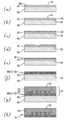
도 2는 도 1의 실시예에 대한 변형을 도시한 개략도의 단면도이다.
도 3은 본 발명에 따른 재분배층 형성을 도시한 개략도이다.
도 4는 실시예 2에서 시험된 중합체의 TGA(공기 중)를 도시한 그래프이다.
도 5는 실시예 2에서 시험된 중합체 1의 TGA(질소 중)를 도시한 그래프이다.
도 6은 실시예 4에서 시험된 바와 같이 제형 1에 의해 생성된 접착선의 SUSS크로크로다일 사진이다. 및
도 7은 실시예 6에 기술된 바와 같이 308nm에서 분리된 블랭크 장치이다.


Claims (49)
- 다음을 포함하는 스택(stack) 구성을 제공하는 단계:
후면 및 전면을 갖는 제1기판;
상기 전면에 인접하고 폴리하이드록시에테르(polyhydroxyether)를 포함하는 접착층; 및
상기 접착층에 인접한 제 1표면을 갖는 제2기판; 및
상기 접착층을 레이저에너지에 노출시켜 상기 제1 및 제2기판의 분리를 용이하게 하는 단계를 포함하는 임시 접착 방법.
- 제1항에 있어서, 상기 폴리하이드록시에테르는 디글리시딜 에테르(diglycidyl ether)와 디하이드록시(dihydroxy)염료의 공중합체를 포함하는 것인 방법.
- 제 2항에 있어서, 상기 디글리시딜 에테르가 비스페놀 A 디글리시딜 에테르(bisphenol A diglycidyl ether), 비스페놀 F 디글리시딜 에테르(bisphenol F diglycidyl ether), 1,4-시클로헥산디메탄올디글리시딜 에테르(1,4-cyclohexanedimethanol diglycidyl ether), 레조르시놀디글리시딜 에테르(resorcinol diglycidyl ether), 비스페놀A 프로폭실레이트 디글리시딜 에테르(bisphenol A propoxylate diglycidyl ether), 에틸렌글리콜디글리시딜 에테르(ethylene glycol diglycidyl ether), 1,4-시클로헥산디메탄올디글리시딜 에테르(1,4-cyclohexandimethanol diglycidyl ether), 글리세롤디글리시딜 에테르(glycerol diglycidyl ether), 1,4-부탄디올디글리시딜 에테르(1,4-butanediol diglycidyl ether), 네오펜틸글리콜디글리시딜 에테르(neopentyl glycol diglycidyl ether), 1,3-부탄디올디글리시딜 에테르(1,3-butanediol diglycidyl ether), 1,3-비스(3-글리시독시프로필)테트라메틸디실록산(1,3-bis(3-glycidoxypropyl)tetramethyldisiloxane), 및 이들의 조합으로 이루어진 군에서 선택되는 것인 방법.
- 제2항에 있어서, 상기 디하이드록시 염료는 4,4'-디하이드록시벤조페논(4,4'-dihydroxybenzophenone), 디하이드록시칼콘 염료(dihydroxy chalcone dyes), 4-[(2-페닐하이드라조노)메틸]레조르시놀(4-[(2-phenylhydrazono)methyl]resorcinol), 디하이드록시아조벤젠(dihydroxyazobenzene), 디하이드록시안트라퀴논(dihydroxyanthraquinone), 2,2'-메틸렌비스[6-(벤조트리아졸-2-일)-4-tert-옥틸페놀](2,2'-methylenebis[6-(benzotriazol-2-yl)-4-tert-octylphenol]), 커큐민(curcumin), 커큐민 유도체(curcumin derivatives), 및 이들의 조합으로 이루어진 군으로부터 선택되는 것인 방법.
- 제1항에 있어서, 상기 접착층은 열가소성층인 방법.
- 제1항에 있어서, 상기 노출은 약 200mJ/cm2 내지 약 400 mJ/cm2의 용량으로 수행되는 것인 방법.
- 제1항에 있어서, 상기 스택을 제공하는 단계는 상기 전면상에 상기 접착층을 형성하는 단계를 포함하는 방법.
- 제7항에 있어서, 상기 형성 단계는 유동성 결합 조성물을 상기 전면에 적용하는 단계를 포함하고, 상기 유동성 조성물은 용매 시스템에 분산 또는 용해된 폴리하이드록시에테르를 포함하는 것인 방법.
- 제8항에 있어서, 상기 조성물은 약 120℃ 내지 약 250℃의 온도에서 약 60초 내지 약 10분 동안 가열하여 상기 접착층을 형성하는 단계를 추가로 포함하는 방법.
- 제7항에 있어서, 상기 형성 단계는 폴리하이드록시에테르를 포함하는 독립형 필름을 상기 전면에 도포하여 상기 접착층을 형성하는 단계를 포함하는 방법.
- 제10항에 있어서, 상기 적용단계는 상기 독립형 필름을 상기 전면에 접착시키는 단계를 포함하는 방법.
- 제1항에 있어서, 상기 전면 및 상기 제1표면 중 하나는;
(1)집적회로로 구성된 그룹으로부터 선택된 장치들의 어레이를 포함하는 장치 표면; MEMS; 마이크로 센서; 전력반도체; 발광 다이오드; 광자회로; 인터포저; 임베디드패시브 디바이스; 및 실리콘, 실리콘-게르마늄, 갈륨 비소 및 질화 갈륨 상에 또는 그로부터 제조된 마이크로디바이스; 및
(2)하기로 이루어진 군으로부터 선택된 하나 이상의 구조를 포함하는 장치 표면:
솔더 법프; 금속포스트; 금속기둥; 및 규소, 폴리실리콘, 이산화 규소, 규소(옥시)질화물, 금속, 저유전율 유전체, 중합체 유전체, 금속 질화물 및 금속 실리사이드로 이루어진 그룹으로부터 선택된 물질로부터 형성되는 방법.
- 제1항에 있어서, 상기 제1 및 제2기판 중 하나는 유리 또는 다른 투명 재료를 포함하는 방법.
- 제1항에 있어서, 상기 제1 및 제2기판을 분리하기 전에 상기 스택에 백그라인딩, 화학-기계적 폴리싱, 에칭, 금속화, 유전체 증착, 패터닝, 패시베이션, 어닐링, 재분배 층 형성 및 이들의 조합으로 이루어진 그룹으로부터 선택된 처리를 수행하는 단계를 더 포함하는 방법.
- 제1항에 있어서, 상기 접착층은 상기 제1기판과 제2기판 사이의 유일한 층인 방법.
- 제1항에 있어서, 상기 접착층은 제1접착력을 가지며, 상기 스택은 상기 제1기판과 제2기판 사이에 제2접착층을 추가로 포함하며, 상기 제2접착층은 상기 제1접착력보다 큰 접착력을 갖는 방법.
- 마이크로 전자 구조물로서:
후면 및 전면을 갖는 제1기판;
상기 전면에 인접하고, 폴리하이드록시에테르를 포함하는 접착층; 및
상기 접착층에 인접한 제1표면을 가지며, 상기 전면 및 상기 제1표면 중 적어도 하나는 장치 표면인 제2기판을 포함하는, 구조물.
- 제17항에 있어서, 상기 폴리하이드록시에테르는 디글리시딜 에테르 및 디하이드록시 염료의 공중합체를 포함하는 마이크로 전자 구조물.
- 제18항에 있어서, 상기 디글리시딜 에테르는 비스페놀 A 디글리시딜 에테르(bisphenol A diglycidyl ether), 비스페놀 F 디글리시딜 에테르(bisphenol F diglycidyl ether), 1,4-시클로헥산디메탄올디글리시딜 에테르(1,4-cyclohexanedimethanol diglycidyl ether), 레조르시놀디글리시딜 에테르(resorcinol diglycidyl ether), 비스페놀A 프로폭실레이트 디글리시딜 에테르(bisphenol A propoxylate diglycidyl ether), 에틸렌글리콜디글리시딜 에테르(ethylene glycol diglycidyl ether), 1,4-시클로헥산디메탄올디글리시딜 에테르(1,4-cyclohexandimethanol diglycidyl ether), 글리세롤디글리시딜 에테르(glycerol diglycidyl ether), 1,4-부탄디올디글리시딜 에테르(1,4-butanediol diglycidyl ether), 네오펜틸글리콜디글리시딜 에테르(neopentyl glycol diglycidyl ether), 1,3-부탄디올디글리시딜 에테르(1,3-butanediol diglycidyl ether), 1,3-비스(3-글리시독시프로필)테트라메틸디실록산(1,3-bis(3-glycidoxypropyl)tetramethyldisiloxane), 및 이들의 조합으로 이루어진 군으로부터 선택되는 마이크로 전자 구조물.
- 제18항에 있어서, 상기 디하이드록시 염료는 4,4'-디하이드록시벤조페논(4,4'-dihydroxybenzophenone), 디하이드록시칼콘 염료(dihydroxy chalcone dyes), 4-[(2-페닐하이드라조노)메틸]레조르시놀(4-[(2-phenylhydrazono)methyl]resorcinol), 디하이드록시아조벤젠(dihydroxyazobenzene), 디하이드록시안트라퀴논(dihydroxyanthraquinone), 2,2'-메틸렌비스[6-(벤조트리아졸-2-일)-4-tert-옥틸페놀](2,2'-methylenebis[6-(benzotriazol-2-yl)-4-tert-octylphenol]), 커큐민(curcumin), 커큐민 유도체(curcumin derivatives), 및 이들의 조함을 이루어진 군으로부터 선택되는 마이크로 전자 구조물.
- 제17항에 있어서, 상기 접착층은 열가소성층인 마이크로 전자 구조물.
- 제17항에 있어서, 상기 접착층의 평균 두께는 약1 μm 내지 약 100 μm인 마이크로 전자 구조물.
- 제 17항에 있어서, 상기 전면 및 상기 제1표면 중 하나는:
(1) 집적회로로 구성된 그룹으로부터 선택된 장치들의 어레이를 포함하는 장치 표면; MEMS; 마이크로 센서; 전력반도체; 발광 다이오드; 광자회로; 인터포저; 임베디드패시브 디바이스; 및 실리콘, 실리콘-게르마늄, 갈륨 비소 및 질화 갈륨 상에 또는 그로부터 제조된 마이크로 디바이스; 및
(2) 하기로 이루어진 군으로부터 선택된 하나 이상의 구조를 포함하는 장치 표면:
솔더 법프; 금속포스트; 금속기둥; 및 규소, 폴리실리콘, 이산화 규소, 규소(옥시)질화물, 금속, 저유전율 유전체, 중합체 유전체, 금속 질화물 및 금속 실리사이드로 이루어진 그룹으로부터 선택된 물질로부터 형성되는 구조물.
- 제17항에 있어서, 상기 제1및 제2기판 중 하나는 유리 또는 다른 투명 재료를 포함하는 마이크로 전자 구조물.
- 제17항에 있어서, 상기 접착층은 상기 제1기판과 제2기판 사이의 유일한 층인 마이크로 전자 구조물.
- 제17항에 있어서, 상기 접착층은 제1접착력을 가지며, 상기 제1 및 제2 기판 사이에 제2접착층을 추가로 포함하고, 상기 제2접착층은 상기 제1접착력보다 큰 접착력을 갖는 것인 마이크로 전자 구조물.
- 마이크로 전자 구조물을 형성하는 방법으로서:
(I) 기판의 표면상에 빌드-업층(build-up layer)을 형성하는 단계로서, 상기 빌드-업층은 폴리하이드록시에테르를 포함하고 상기 기판의 표면으로부터 이격된 상부 표면을 갖는 단계;
(II) 상기 상부 표면 상에 제1재분배층을 형성하는 단계; 및
(III) 선택적으로 상기 제1재분배층상에 하나 이상의 추가 재분배층을 형성하는 단계를 포함하는 방법.
- 제27항에 있어서 다음을 더 포함하는 것인:
(IV) 마지막 재분배층 형성하는 단계(II) 및 선택적으로 형성하는 단계(III)에 솔더 볼(solder ball)을 부착하는 단계;
(V) 다이(die)를 상기 솔더 볼에 부착하는 단계; 및
(VI) 선택적으로 부착하는 단계(IV) 및 부착하는 단계(V)을 1회이상 반복하는 단계를 더 포함하는 것인 방법.
- 제28항에 있어서, 상기 기판상에 팬-아웃 웨이퍼 레벨 패키지(fan-out wafer level pakage) 구조를 형성하기 위해 상기 다이 및 솔더 볼 위에 에폭시층을 형성하는 단계를 더 포함하는 방법.
- 제29항에 있어서, 상기 기판과 상기 팬-아웃 웨이퍼 러벨 패키지 구조를 분리하는 단계를 더 포함하는 방법.
- 제30항에 있어서, 상기 분리단계는 상기 기판 및 상기 팬-아웃 웨이퍼 레벨 패키지 구조의 분리를 용이하게 하기 위해 상기 빌드-업 층을 레이저 에너지에 노출시키는 단계를 포함하는 방법.
- 제31항에 있어서, 노출 시키는 단계가 약 200 mJ/cm2 내지 약 400 mJ/cm2의 용량으로 수행되는 방법.
- 제 27항에 있어서, 상기 폴리하이드록시에테르는 디글리시딜 에테르(diglycidyl ether) 및 디하이드록시 염료(dihydroxy dye)의 공중합체를 포함하는 것인 방법.
- 제33항에 있어서, 상기 디글리시딜 에테르가 비스페놀 A 디글리시딜에테르(bisphenol A diglycidyl ether), 비스페놀 F 디글리시딜에테르(bisphenol F diglycidyl ether), 1,4-시클로헥산디메탄올디글리시딜에테르(1,4-cyclohexanedimethanol diglycidyl ether), 레조르시놀디글리시딜에테르(resorcinol diglycidyl ether), 비스페놀A 프로폭실레이트 디글리시딜에테르(bisphenol A propoxylate diglycidyl ether), 에틸렌글리콜디글리시딜에테르(ethylene glycol diglycidyl ether), 1,4-시클로헥산디메탄올디글리시딜에테르(1,4-cyclohexandimethanol diglycidyl ether), 글리세롤디글리시딜에테르(glycerol diglycidyl ether), 1,4-부탄디올디글리시딜에테르(1,4-butanediol diglycidyl ether), 네오펜틸글리콜디글리시딜에테르(neopentyl glycol diglycidyl ether), 1,3-부탄디올디글리시딜에테르(1,3-butanediol diglycidyl ether), 1,3-비스(3-글리시독시프로필)테트라메틸디실록산(1,3-bis(3-glycidoxypropyl)tetramethyldisiloxane), 및 이들의 조합으로 이루어진 군에서 선택되는 것인 방법.
- 제33항에 있어서, 상기 디하이드록시 염료가 4,4'-디하이드록시벤조페논(4,4'-dihydroxybenzophenone), 디하이드록시칼콘 염료(dihydroxy chalcone dyes), 4-[(2-페닐하이드라조노)메틸]레조르시놀(4-[(2-phenylhydrazono)methyl]resorcinol), 디하이드록시아조벤젠(dihydroxyazobenzene), 디하이드록시안트라퀴논(dihydroxyanthraquinone), 2,2'-메틸렌비스[6-(벤조트리아졸-2-일)-4-tert-옥틸페놀](2,2'-methylenebis[6-(benzotriazol-2-yl)-4-tert-octylphenol]), 커큐민(curcumin), 커큐민 유도체(curcumin derivatives), 및 이들의 조합으로 이루어진 군에서 선택되는 것인 방법.
- 제27항에 있어서, 상기 (I)형성단계는 유동성 조성물을 상기 기판의 표면에 적용하는 단계를 포함하고, 상기 유동성 조성물은 용매 시스템에 분산 또는 용해된 상기 폴리하이드록시에테르를 포함하는 것인 방법.
- 제36항에 있어서, 상기 빌드-업층을 형성하기 위해 약 60초 내지 약 10분의 시간 동안 약 120℃ 내지 250℃의 온도에서 상기 조성물을 가열하는 단계를 포함하는 방법.
- 제27항에 있어서, 상기 (I)형성하는 단계는 상기 폴리하이드록시에테르를 포함하는 독립형 필름을 상기 기판의 표면에 도포하여 상기 빌드-업층을 형성하는 단계를 포함하는 방법.
- 제38항에 있어서, 상기 적용단계는 상기 독립형 필름을 상기 기판의 표면에 접착시키는 단계를 포함하는 방법.
- 제27항에 있어서, 상기 기판은 유리 또는 다른 투명재료를 포함하는 방법.
- 제27항에 있어서, 다음을 더 포함하는 것인:
형성하는 단계(II) 및 선택적으로 형성하는 단계(III)의 마지막 재분배층에 다수의 솔더 볼을 부착하는 단계; 및
상기 다수의 솔더 볼 중 적어도 2개에 다이(die)를 부착하는 단계를 더 포함하는 방법.
- 다음을 포함하는 마이크로 전자 구조체:
표면을 갖는 기판;
기판 표면상의 빌드-업 층 상기 빌드-업 층은 폴리하이드록시에테르를 포함하고 상기 기판 표면으로부터 멀리 떨어진 상부 표면을 갖고; 및
상기 상부 표면상의 제1재분배 층.
- 제42항에 있어서, 상기 제1재분배층 상에 하나 이상의 추가 재분배층을 추가로 포함하는 구조체.
- 제42항에 있어서, 상기 제1재분배층 상에 적어도 하나의 솔더 볼 및 상기 적어도 하나의 솔더 볼에 부착된 다이를 더 포함하는 구조체.
- 제44항에 있어서, 상기 솔더 볼 및 다이 위에 에폭시 코팅을 추가로 포함하는 구조체.
- 제42항에 있어서, 상기 폴리하이드록시에테르는 디글리시딜 에테르 및 디하이드록시 염료의 공중합체를 포함하는 것인 구조체.
- 제46항에 있어서, 상기 디글리시딜 에테르가 비스페놀 A 디글리시딜에테르(bisphenol A diglycidyl ether), 비스페놀 F 디글리시딜에테르(bisphenol F diglycidyl ether), 1,4-시클로헥산디메탄올디글리시딜에테르(1,4-cyclohexanedimethanol diglycidyl ether), 레조르시놀디글리시딜에테르(resorcinol diglycidyl ether), 비스페놀A 프로폭실레이트 디글리시딜에테르(bisphenol A propoxylate diglycidyl ether), 에틸렌글리콜디글리시딜에테르(ethylene glycol diglycidyl ether), 1,4-시클로헥산디메탄올디글리시딜에테르(1,4-cyclohexandimethanol diglycidyl ether), 글리세롤디글리시딜에테르(glycerol diglycidyl ether), 1,4-부탄디올디글리시딜에테르(1,4-butanediol diglycidyl ether), 네오펜틸글리콜디글리시딜에테르(neopentyl glycol diglycidyl ether), 1,3-부탄디올디글리시딜에테르(1,3-butanediol diglycidyl ether), 1,3-비스(3-글리시독시프로필)테트라메틸디실록산(1,3-bis(3-glycidoxypropyl)tetramethyldisiloxane), 및 이들의 조합으로 이루어진 군에서 선택되는 것인 구조체.
- 제46항에 있어서, 상기 디하이드록시 염료는 4,4'-디하이드록시벤조페논(4,4'-dihydroxybenzophenone), 디하이드록시칼콘 염료(dihydroxy chalcone dyes), 4-[(2-페닐하이드라조노)메틸]레조르시놀(4-[(2-phenylhydrazono)methyl]resorcinol), 디하이드록시아조벤젠(dihydroxyazobenzene), 디하이드록시안트라퀴논(dihydroxyanthraquinone), 2,2'-메틸렌비스[6-(벤조트리아졸-2-일)-4-tert-옥틸페놀](2,2'-methylenebis[6-(benzotriazol-2-yl)-4-tert-octylphenol]), 커큐민(curcumin), 커큐민 유도체(curcumin derivatives), 및 이들의 조합으로 이루어진 군에서 선택되는 것인 구조체.
- 제42항에 있어서, 상기 제1및 제2기판 중 하나는 유리 또는 다른 투명재료를 포함하는 구조체.
Applications Claiming Priority (3)
| Application Number | Priority Date | Filing Date | Title |
|---|---|---|---|
| US201762609426P | 2017-12-22 | 2017-12-22 | |
| US62/609,426 | 2017-12-22 | ||
| PCT/US2018/067099 WO2019126648A1 (en) | 2017-12-22 | 2018-12-21 | Laser-releasable bonding materials for 3-d ic applications |
Publications (2)
| Publication Number | Publication Date |
|---|---|
| KR20200092349A true KR20200092349A (ko) | 2020-08-03 |
| KR102700016B1 KR102700016B1 (ko) | 2024-08-28 |
Family
ID=66949543
Family Applications (1)
| Application Number | Title | Priority Date | Filing Date |
|---|---|---|---|
| KR1020207018152A Active KR102700016B1 (ko) | 2017-12-22 | 2018-12-21 | 3-d ic응용 제품을 위한 레이저로 분리 가능한 접착 재료 |
Country Status (8)
| Country | Link |
|---|---|
| US (1) | US10968348B2 (ko) |
| EP (1) | EP3727838B1 (ko) |
| JP (1) | JP7362612B2 (ko) |
| KR (1) | KR102700016B1 (ko) |
| CN (1) | CN111556807B (ko) |
| SG (1) | SG11202005465SA (ko) |
| TW (1) | TWI827574B (ko) |
| WO (1) | WO2019126648A1 (ko) |
Families Citing this family (12)
| Publication number | Priority date | Publication date | Assignee | Title |
|---|---|---|---|---|
| US10490525B1 (en) * | 2018-05-10 | 2019-11-26 | International Business Machines Corporation | High speed handling of ultra-small chips by selective laser bonding and debonding |
| US11073572B2 (en) * | 2019-01-17 | 2021-07-27 | Infineon Technologies Ag | Current sensor device with a routable molded lead frame |
| WO2020154225A1 (en) * | 2019-01-22 | 2020-07-30 | Brewer Science, Inc. | Laser-releasable bonding materials for 3-d ic applications |
| CN110396404B (zh) * | 2019-07-12 | 2022-06-17 | 新乡医学院 | 基于腙类衍生物的荧光分子探针及其制备方法和在阳离子识别方面的应用 |
| EP4007799A4 (en) * | 2019-08-02 | 2023-09-06 | Brewer Science Inc. | Permanent bonding and patterning material |
| KR102790889B1 (ko) | 2020-01-02 | 2025-04-04 | 삼성전자주식회사 | 반도체 패키지와 이를 구비하는 전자 장치 및 반도체 패키지의 제조방법 |
| US12024594B2 (en) * | 2020-04-27 | 2024-07-02 | Brewer Science, Inc. | Multifunctional materials for temporary bonding |
| WO2021235406A1 (ja) | 2020-05-21 | 2021-11-25 | デンカ株式会社 | 組成物 |
| CN116018675A (zh) * | 2020-08-14 | 2023-04-25 | 布鲁尔科技公司 | 永久性粘结和图案化材料 |
| KR20230147115A (ko) * | 2021-02-15 | 2023-10-20 | 브레우어 사이언스, 인코포레이션 | 열압착 본딩에서 금속 연결의 변형을 방지하기 위한 임시 본딩 및 디본딩 공정 |
| KR20230067337A (ko) | 2021-11-09 | 2023-05-16 | 삼성전자주식회사 | 반도체 패키지 및 그 제조 방법 |
| US12588521B2 (en) * | 2023-02-15 | 2026-03-24 | Wolfspeed, Inc. | Metal nitride core-shell particle die-attach material |
Citations (5)
| Publication number | Priority date | Publication date | Assignee | Title |
|---|---|---|---|---|
| JP2003078117A (ja) * | 2001-08-31 | 2003-03-14 | Canon Inc | 半導体部材及び半導体装置並びにそれらの製造方法 |
| US20130288058A1 (en) * | 2012-04-30 | 2013-10-31 | Brewer Science Inc. | Development of high-viscosity bonding layer through in-situ polymer chain extension |
| US20150115456A1 (en) * | 2011-12-30 | 2015-04-30 | Deca Technologies, Inc. | Die up fully molded fan-out wafer level packaging |
| WO2016071788A1 (en) * | 2014-11-07 | 2016-05-12 | International Business Machines Corporation | Low temperature adhesive resins for wafer bonding |
| KR20170039187A (ko) * | 2014-07-22 | 2017-04-10 | 브레우어 사이언스 인코포레이션 | 3차원 ic 적용용 레이저 박리 재료로서의 폴리이미드 |
Family Cites Families (16)
| Publication number | Priority date | Publication date | Assignee | Title |
|---|---|---|---|---|
| US5989700A (en) * | 1996-01-05 | 1999-11-23 | Tekscan Incorporated | Pressure sensitive ink means, and methods of use |
| US7052597B2 (en) * | 2001-03-27 | 2006-05-30 | Exxonmobil Research And Engineering Company | Tuning fuel composition for driving cycle conditions in spark ignition engines |
| DE502006000292D1 (de) * | 2005-03-22 | 2008-03-06 | Ems Chemie Ag | Aus einem Polyhydroxyether enthaltenden Rohstoff gesponnenes thermoplastisches Fasermaterial, Verfahren zu seiner Herstellung und Verwendungen dafür |
| US9111981B2 (en) | 2008-01-24 | 2015-08-18 | Brewer Science Inc. | Method for reversibly mounting a device wafer to a carrier substrate |
| CN101393400B (zh) * | 2008-10-29 | 2011-12-14 | 清溢精密光电(深圳)有限公司 | 液体感光性树脂凸版表面除粘方法 |
| US8859672B2 (en) * | 2011-06-27 | 2014-10-14 | Sabic Global Technologies B.V. | Poly(arylene ether)-poly(hydroxy ether) block copolymer and method of making |
| US9827757B2 (en) * | 2011-07-07 | 2017-11-28 | Brewer Science Inc. | Methods of transferring device wafers or layers between carrier substrates and other surfaces |
| JP2015021082A (ja) * | 2013-07-19 | 2015-02-02 | 日東電工株式会社 | 電子部品切断用熱剥離型粘着テープおよび電子部品の切断方法 |
| US9865490B2 (en) * | 2014-01-07 | 2018-01-09 | Brewer Science Inc. | Cyclic olefin polymer compositions and polysiloxane release layers for use in temporary wafer bonding processes |
| US9496164B2 (en) * | 2014-01-07 | 2016-11-15 | Brewer Science Inc. | Cyclic olefin polymer compositions and polysiloxane release layers for use in temporary wafer bonding processes |
| US9850406B2 (en) * | 2014-11-07 | 2017-12-26 | International Business Machines Corporation | Adhesive resins for wafer bonding |
| US10522383B2 (en) * | 2015-03-25 | 2019-12-31 | International Business Machines Corporation | Thermoplastic temporary adhesive for silicon handler with infra-red laser wafer de-bonding |
| JP7356902B2 (ja) | 2016-07-15 | 2023-10-05 | ブルーワー サイエンス アイ エヌ シー. | レーザーアブレーションの誘電性物質 |
| US10617010B2 (en) | 2016-08-29 | 2020-04-07 | Brewer Science, Inc. | Polymer film stencil process for fan-out wafer-level packaging of semiconductor devices |
| US10217637B1 (en) * | 2017-09-20 | 2019-02-26 | International Business Machines Corporation | Chip handling and electronic component integration |
| KR20200079313A (ko) * | 2017-11-08 | 2020-07-02 | 사이텍 인더스트리스 인코포레이티드 | 층간 강인화 입자를 갖는 복합체 및 이의 제조 방법 |
-
2018
- 2018-12-21 CN CN201880082753.8A patent/CN111556807B/zh active Active
- 2018-12-21 SG SG11202005465SA patent/SG11202005465SA/en unknown
- 2018-12-21 JP JP2020531625A patent/JP7362612B2/ja active Active
- 2018-12-21 KR KR1020207018152A patent/KR102700016B1/ko active Active
- 2018-12-21 WO PCT/US2018/067099 patent/WO2019126648A1/en not_active Ceased
- 2018-12-21 EP EP18893305.5A patent/EP3727838B1/en active Active
- 2018-12-21 TW TW107146370A patent/TWI827574B/zh active
- 2018-12-21 US US16/229,591 patent/US10968348B2/en active Active
Patent Citations (5)
| Publication number | Priority date | Publication date | Assignee | Title |
|---|---|---|---|---|
| JP2003078117A (ja) * | 2001-08-31 | 2003-03-14 | Canon Inc | 半導体部材及び半導体装置並びにそれらの製造方法 |
| US20150115456A1 (en) * | 2011-12-30 | 2015-04-30 | Deca Technologies, Inc. | Die up fully molded fan-out wafer level packaging |
| US20130288058A1 (en) * | 2012-04-30 | 2013-10-31 | Brewer Science Inc. | Development of high-viscosity bonding layer through in-situ polymer chain extension |
| KR20170039187A (ko) * | 2014-07-22 | 2017-04-10 | 브레우어 사이언스 인코포레이션 | 3차원 ic 적용용 레이저 박리 재료로서의 폴리이미드 |
| WO2016071788A1 (en) * | 2014-11-07 | 2016-05-12 | International Business Machines Corporation | Low temperature adhesive resins for wafer bonding |
Also Published As
| Publication number | Publication date |
|---|---|
| EP3727838A1 (en) | 2020-10-28 |
| EP3727838B1 (en) | 2023-08-09 |
| SG11202005465SA (en) | 2020-07-29 |
| TW201934692A (zh) | 2019-09-01 |
| CN111556807B (zh) | 2023-09-08 |
| US10968348B2 (en) | 2021-04-06 |
| KR102700016B1 (ko) | 2024-08-28 |
| JP2021508168A (ja) | 2021-02-25 |
| EP3727838A4 (en) | 2021-08-18 |
| WO2019126648A1 (en) | 2019-06-27 |
| US20190194453A1 (en) | 2019-06-27 |
| JP7362612B2 (ja) | 2023-10-17 |
| CN111556807A (zh) | 2020-08-18 |
| TWI827574B (zh) | 2024-01-01 |
Similar Documents
| Publication | Publication Date | Title |
|---|---|---|
| KR102700016B1 (ko) | 3-d ic응용 제품을 위한 레이저로 분리 가능한 접착 재료 | |
| US20250282979A1 (en) | Photonic debonding for wafer-level packaging applications | |
| US9827740B2 (en) | Polyimides as laser release materials for 3-D IC applications | |
| US20230187257A1 (en) | Laser-releasable bonding materials for 3-d ic applications | |
| KR20140039330A (ko) | 박형 웨이퍼 핸들링을 위한 다중 본딩 층 | |
| US20210332188A1 (en) | Multifunctional materials for temporary bonding | |
| US20250132283A1 (en) | Versatile dual-layer temporary wafer bonding for harsh processing conditions | |
| EP4197028A1 (en) | Permanent bonding and patterning material |
Legal Events
| Date | Code | Title | Description |
|---|---|---|---|
| PA0105 | International application |
St.27 status event code: A-0-1-A10-A15-nap-PA0105 |
|
| P11-X000 | Amendment of application requested |
St.27 status event code: A-2-2-P10-P11-nap-X000 |
|
| P13-X000 | Application amended |
St.27 status event code: A-2-2-P10-P13-nap-X000 |
|
| PG1501 | Laying open of application |
St.27 status event code: A-1-1-Q10-Q12-nap-PG1501 |
|
| PN2301 | Change of applicant |
St.27 status event code: A-3-3-R10-R13-asn-PN2301 St.27 status event code: A-3-3-R10-R11-asn-PN2301 |
|
| A201 | Request for examination | ||
| P11-X000 | Amendment of application requested |
St.27 status event code: A-2-2-P10-P11-nap-X000 |
|
| P13-X000 | Application amended |
St.27 status event code: A-2-2-P10-P13-nap-X000 |
|
| PA0201 | Request for examination |
St.27 status event code: A-1-2-D10-D11-exm-PA0201 |
|
| E13-X000 | Pre-grant limitation requested |
St.27 status event code: A-2-3-E10-E13-lim-X000 |
|
| P11-X000 | Amendment of application requested |
St.27 status event code: A-2-2-P10-P11-nap-X000 |
|
| P13-X000 | Application amended |
St.27 status event code: A-2-2-P10-P13-nap-X000 |
|
| D13-X000 | Search requested |
St.27 status event code: A-1-2-D10-D13-srh-X000 |
|
| D14-X000 | Search report completed |
St.27 status event code: A-1-2-D10-D14-srh-X000 |
|
| E902 | Notification of reason for refusal | ||
| PE0902 | Notice of grounds for rejection |
St.27 status event code: A-1-2-D10-D21-exm-PE0902 |
|
| T11-X000 | Administrative time limit extension requested |
St.27 status event code: U-3-3-T10-T11-oth-X000 |
|
| E13-X000 | Pre-grant limitation requested |
St.27 status event code: A-2-3-E10-E13-lim-X000 |
|
| P11-X000 | Amendment of application requested |
St.27 status event code: A-2-2-P10-P11-nap-X000 |
|
| P13-X000 | Application amended |
St.27 status event code: A-2-2-P10-P13-nap-X000 |
|
| E701 | Decision to grant or registration of patent right | ||
| PE0701 | Decision of registration |
St.27 status event code: A-1-2-D10-D22-exm-PE0701 |
|
| PR0701 | Registration of establishment |
St.27 status event code: A-2-4-F10-F11-exm-PR0701 |
|
| PR1002 | Payment of registration fee |
St.27 status event code: A-2-2-U10-U12-oth-PR1002 Fee payment year number: 1 |
|
| PG1601 | Publication of registration |
St.27 status event code: A-4-4-Q10-Q13-nap-PG1601 |
|
| P22-X000 | Classification modified |
St.27 status event code: A-4-4-P10-P22-nap-X000 |