US6161159A - Multimedia computer with integrated circuit memory - Google Patents
Multimedia computer with integrated circuit memory Download PDFInfo
- Publication number
- US6161159A US6161159A US08/936,918 US93691897A US6161159A US 6161159 A US6161159 A US 6161159A US 93691897 A US93691897 A US 93691897A US 6161159 A US6161159 A US 6161159A
- Authority
- US
- United States
- Prior art keywords
- variable
- data
- memory
- port
- integrated circuit
- Prior art date
- Legal status (The legal status is an assumption and is not a legal conclusion. Google has not performed a legal analysis and makes no representation as to the accuracy of the status listed.)
- Expired - Fee Related
Links
Images


Classifications
-
- G—PHYSICS
- G06—COMPUTING OR CALCULATING; COUNTING
- G06F—ELECTRIC DIGITAL DATA PROCESSING
- G06F1/00—Details not covered by groups G06F3/00 - G06F13/00 and G06F21/00
-
- G—PHYSICS
- G09—EDUCATION; CRYPTOGRAPHY; DISPLAY; ADVERTISING; SEALS
- G09G—ARRANGEMENTS OR CIRCUITS FOR CONTROL OF INDICATING DEVICES USING STATIC MEANS TO PRESENT VARIABLE INFORMATION
- G09G5/00—Control arrangements or circuits for visual indicators common to cathode-ray tube indicators and other visual indicators
- G09G5/36—Control arrangements or circuits for visual indicators common to cathode-ray tube indicators and other visual indicators characterised by the display of a graphic pattern, e.g. using an all-points-addressable [APA] memory
- G09G5/39—Control of the bit-mapped memory
-
- G—PHYSICS
- G09—EDUCATION; CRYPTOGRAPHY; DISPLAY; ADVERTISING; SEALS
- G09G—ARRANGEMENTS OR CIRCUITS FOR CONTROL OF INDICATING DEVICES USING STATIC MEANS TO PRESENT VARIABLE INFORMATION
- G09G2360/00—Aspects of the architecture of display systems
- G09G2360/12—Frame memory handling
- G09G2360/122—Tiling
-
- G—PHYSICS
- G09—EDUCATION; CRYPTOGRAPHY; DISPLAY; ADVERTISING; SEALS
- G09G—ARRANGEMENTS OR CIRCUITS FOR CONTROL OF INDICATING DEVICES USING STATIC MEANS TO PRESENT VARIABLE INFORMATION
- G09G2360/00—Aspects of the architecture of display systems
- G09G2360/12—Frame memory handling
- G09G2360/125—Frame memory handling using unified memory architecture [UMA]
Definitions
- the present invention relates in general to highspeed computers, and relates in particular to a computer for processing a large volume of data such as image data and other multimedia applications, and an integrated circuit memory designed for improved speed of processing to be used with the computer.
- FIG. 8 An example of the configuration of a conventional small computer is shown in FIG. 8.
- Mathematical computation and signal processing are performed by combined actions of a microprocessor 1 connected to the main memory 2 by way of a bus•memory controller 3.
- Input data are supplied from an input/output (I/O) device 5, through a system bus 7, to the bus•memory controller 3.
- the I/O device 5 is connected to a communication port (comport) 8, and performs data transmitting and receiving tasks for the communication circuit and the computer.
- the I/O device 5 is connected with secondary memory devices 10, such as hard disk and floppy disk, and input devices 11 such as a keyboard and a mouse.
- the results of computations generated by the microprocessor 1 are supplied, through the system bus 7, to the video controller 4, and are stored in a frame buffer 9.
- the data stored in the frame buffer 9 are displayed in real time on a monitor 6 under the control of the video controller 4.
- the frame buffer is a type of (semiconductor) memory for storing current data.
- FIG. 9 shows another example of the system configuration of a conventional computer.
- the current image data are stored in a section of the main memory 2.
- the components other than the frame buffer, such as input section and computation section, are the same as those shown in FIG. 8. The cost of the system is reduced because of lesser number of required component parts.
- the circuit components used for main memory 2 and frame buffer 9 are integrated circuits, such as the one shown schematically in FIG. 10.
- the data are stored in memory cell array 20 comprised by several mega bits to several tens of mega bits of memory cells.
- a memory cell is specified by an address in the memory cell array.
- An address is given in the binary notation from the address port 27, and an address decoder 21 is used to specify a memory cell or a group of memory cells.
- Data are written into the memory cells from the data port 26, by way of a buffer 23.
- the contents of the memory are read by the sense amplifier 22, and are output to the data port.
- a dedicated integrated circuit a video RAM, is sometimes used for the frame buffer.
- a video RAM stores a group of data read out by the sense amplifier 22 in the data buffer 32, and reads the data from the data buffer 32 one bit at a time from the data port 26' according to an address signal prompted by a counter 33 operating at the clock frequency generated by clock input means 34.
- the data port 26' serves as the data output terminal to the monitor 6.
- a computer system having a dedicated video memory is assembled so that the monitor 6 is connected to the frame buffer 9 by way of an digital-to-analogue converter (D/A converter) 12.
- D/A converter digital-to-analogue converter
- an D/A converter 12 is included in the video controller 4, but the D/A converter 12 is shown separately from the video controller 4 in FIG. 12, because such an integral dedicated memory has a separate video output port, as in the example in FIG. 12.
- the process of decompressing the compressed image data signals will be explained with reference to a flowchart shown in FIG. 13.
- the image signals delivered from a communication circuit or a recording medium are separated into image data component, motion vector components and quantizer indexes, in the signal separation task 50.
- the image data are already encoded into variable-length words according to such methods as Huffman encoding, for example, and are decoded in the variable-length word decoding task 51.
- the reverse quantization processing task 52 which follows, the original signals are restored using the quantizer table.
- the quantizer table is included in the delivered signals, and are separated during the process of signal separation.
- the frequency components are converted to real space components.
- frame-to-frame sequence data are processed using the motion vector (obtained in the signal separation task 50) in the motion compensation task 56, and then the sequence data are added in the adder 54 to the image data processed by the DCT processing task 53, to restore the original images.
- the rearranging processing task 55 rearranges the image data in the chronological sequence, to restore the true image data from the compressed image data.
- the restored data are delivered, as new image data, to the image accumulation processing task 57 and form the basis for compensating the next image movement.
- image processing is performed as follows. First, image data are input from the com port 8, by way of the I/O device 5, system bus 7, and bus•memory controller 3, to be stored in the main memory 2. The necessary portions of the image data in the main memory 2 are written into the micro-processor 1 and the series of processes depicted in FIG. 13 are performed. The final image data are stored in the main memory 2 to be ready for the image accumulation task 57 and image rearranging task 55 (refer to FIG. 13), as well as being written into the frame buffer 9, by way of the bus•memory controller 3 and the video controller 4. The data in the frame buffer 9 are displayed on the monitor 6 under the control of the video controller 4.
- various tasks such as reading out necessary data from the main memory and writing data temporarily into the main memory continue to be performed.
- the programs necessary to perform such tasks are also stored in the main memory, and necessary sections of the program are read into the microprocessor while the image processing processes are being carried out.
- the image data are handled in units called a macro-block comprised roughly by 8 ⁇ 8 pixels, and are processed as an 8-bit matrix.
- the reverse quantizer task 52 and the reverse DCT task 53 are performed in matrix multiplications, and the signal addition task 54 performs matrix additions. These operations are performed by repeating the same types of computations, and computations can be made faster by using parallel processing devices. Recently, microprocessors having parallel processing pipelines are being applied to computers to enhance their image processing capability.
- variable-length encoding task 51 compares input data with the table and converts the input data to corresponding data. Because the bit length in the table are different depending on the encoding mode, it is not possible to find the start of the next word unless the previous word has been decoded. Therefore, the input signals must be examined serially, and consequently, they are not amenable to parallel processing. It can not be anticipated, therefore, that speed enhancement in the variable-length encoding process can be achieved through the use of parallel processing devices.
- the first problem is that, in the conventional image processing technology, a microprocessor and memories are constituted by separate independent integrated circuits, and a bottleneck in the processing speed occurs in the slow process of data exchange between these two components of the computer system.
- the second problem is that, in the conventional computers, volume of image data which must be handled in a series of operations can sometimes be beyond the processing capacity of a given type of microprocessor.
- the third problem is that when the performance of the conventional image processing computers are improved, there is a tendency for the computer system to become higher priced.
- main memory means having an access port for a microprocessor and an input port for inputting data directly from an input/output device.
- the object has also be achieved in a computer system comprising at least: a microprocessor connected to a bus•memory controller; a video controller connected to the bus•memory controller through main memory means and a system bus; and an input/output device.
- An aspect of the computer system presented above is that, in addition to an access port for a microprocessor, a direct access port is provided for directly accessing the main memory means through an input/output device.
- the object has been also achieved in a computer system comprising main memory means for performing functions of directly writing into the main memory means through a write port and of decoding variable-length encoded signals within the main memory means.
- the object is achieved by applying to the computer system an integrated circuit memory, having a computational ability, comprising an address port for accessing by a microprocessor; a first data port; a second data port for inputting variable-length encoded signals.
- An aspect of the integrated circuit memory is that a decoder for performing variable-length computational operations is provided.
- decoder decodes the variable-length encoded signals, in reference to a decoding table associated with memory cells.
- an integrated circuit memory having a computational ability, comprising at least: a memory cell array; an address decoder for decoding memory cell addresses for data input from an address port; a sense amplifier for amplifying signals from memory cells; and a write-buffer for writing data input from a first data port into memory cells; wherein a second data port is provided for inputting variable-length encoded signals.
- An aspect of the integrated circuit memory presented above is that a decoder is provided for performing computations based on variable-length encoded signals.
- An aspect of the integrated circuit memory presented above is that the decoder performs decoding operations in reference to a decoding table associated with memory cells.
- an integrated circuit memory having a computational ability, comprising: an address port for accessing by a microprocessor; a first data port; a second data port for outputting data; and a third data port for inputting variable-length encoded signals.
- An aspect of the integrated circuit memory presented above is that a decoder is provided for performing computations based on variable-length encoded signals.
- An aspect of the integrated circuit memory presented above is that the decoder performs decoding operations in reference to a decoding table associated with memory cells.
- an integrated circuit memory having a computational ability, comprising at least: a memory cell array; an address decoder for decoding memory cell addresses for data input from an address port; a sense amplifier for amplifying signals from memory cells; and a write-buffer for writing data input from a first data port into memory cells; wherein a second data port for outputting data and a third data port for inputting variable-length encoded signals are provided.
- An aspect of the integrated circuit memory presented above is that a decoder is provided for performing computations based on variable-length encoded signals.
- An aspect of the integrated circuit memory presented above is that the decoder performs decoding operations in reference to a decoding table associated with memory cells.
- a first advantage presented is that the volume of data that need to be exchanged between the main memory and the microprocessor has been greatly reduced.
- the reason is that the IC memory provided in the main memory is used to decode the variable-length encoded image data so that the need to decode, by forwarding programs and data for image data processing from the main memory to the microprocessor, has been eliminated.
- This portion of the overall processing task is about twenty to thirty percent, and the IC memory has enabled to eliminate almost all of the needs for this transference task.
- a second advantage presented is that the volume of data that the microprocessor must manipulate for image processing has been reduced.
- the microprocessor having a parallel onboard computation device is able to efficiently process such series of image processing tasks as quantization, reverse quantization cosine conversion and motion anticipation; however, other tasks such as variable-length decoding, that are difficult to be processed by the parallel processor, are assigned to the main memory having the IC memory of the present invention.
- the result of this re-assignment of responsibility is that the microprocessor is no longer called upon to perform tasks which are inefficiently processed in the microprocessor.
- a third advantage presented is that an image processing computer system can be produced at a lower cost. The reason is that almost all of the component requirements in the computer system can be met by standardized component parts, thus enabling to contain the needs for increasing number of additional components.
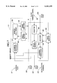
- FIG. 1 is a schematic block diagram of the system configuration of an embodiment of the computer system of the present invention.
- FIG. 2 is a schematic block diagram of the component configuration of the first embodiment of IC memory.
- FIG. 3 is a schematic block diagram of the component configuration of another embodiment of IC memory.
- FIG. 4 is a schematic block diagram of the component configuration of still anther embodiment of the computer system of the present invention.
- FIG. 5 is a schematic block diagram of the system configuration of still another embodiment of the computer system.
- FIG. 6 is a schematic block diagram of the component configuration of still another embodiment of the IC memory.
- FIG. 7 is a schematic block diagram of the component configuration of still another embodiment of the IC memory.
- FIG. 8 is a schematic block diagram of the system configuration of a conventional computer system.
- FIG. 9 is a schematic block diagram of the system configuration of another conventional computer system.
- FIG. 10 is a schematic block diagram of the component configuration of a conventional IC memory.
- FIG. 11 is a schematic block diagram of the component configuration of still another conventional IC memory.
- FIG. 12 is a schematic block diagram of the system configuration of still another conventional computer system.
- FIG. 13 is a flowchart for processing of compressed image data by a computer system.
- a first embodiment computer system features a main memory 2 (commonly referred to as memory boards) which is provided with a separate port for connecting the I/O device 5'.
- the main memory 2 stores image data, application programs, and currently displayed image data.
- the other port on the main memory 2 is the same as the conventional port and is connected to the microprocessor 1 by way of the bus•memory controller 3.
- the bus•memory controller 3 is connected to the video controller 4 through the system bus 7, and the video controller 4 is connected to the main memory 2 and the monitor 6.
- the secondary memory 10 and input devices 11, such as keyboard, are connected to the bus•memory controller 3, micro-processor 1 and main memory 2 by way of the I/O device 5 connected to the system bus 7.
- FIG. 2 shows a structure of the IC memory comprising the main memory 2 whose data port 28 is connected to the I/O device 5'.
- the image data input into the memory circuit 31 are decoded by a decoder 24, having a computation capability for variable-length decoding, and are written into a memory cell array 20 by way of a write-buffer 23.
- An address generator 25 generates write-addresses for decoded image data, and by way of the address decoder, specifies write-addresses for the memory cells.
- initializing signals for initializing the address generator 25 are input from the initialization terminal 29.
- Microprocessor 1 accesses and specifies memory cell addresses through the address port 27 and the address decoder 21, writes into the memory cells by way of the data port 26 and the write-buffer 23, and reads data at the data port 26 by way of the sense amplifier 22.
- the address generator 25 in the memory circuit 31 is initialized by generating initializing signals 29 from the computer.
- Image signals compressed as variable-length encoded data are input from the com port 8.
- the image data are written into the main memory 2 of the computer by the I/O device 5', and are input into the IC memory from the data port 28 of the main memory 2.
- the input image data are first subjected to variable-length decoding computation by the decoder 24.
- the decoded image data are written, by way of the write-buffer 23, into the memory cell array 22 by the decoder 24.
- the decoder 24 generates a request signal to the address generator 25 for an address to write in the image data, and in response, the address generator 25 specifies a memory cell for the image data by way of the address decoder 21.
- the variable-length encoded image data input from the com port 8 are decoded and written into the memory cell in variable-length words.
- This IC memory can be fabricated by adding a serial input data port 28 and signal control circuits, such as initialization circuit 29, to any general-purpose memory device, and consequently, what is required are some additional pins to an existing IC pattern.
- the microprocessor 1 accesses the processed image data in the main memory 2 by way of the bus•memory controller 3, and performs a series of subsequent image processing tasks other than the variable-length decoding task (which is performed by the decoder 24 in main memory 2) while exchanging in-process data and final data and others between itself and the main memory 2. Therefore, it can be seen that a computer can perform all the necessary tasks in a conventional manner, excepting the variable-length decoding task.
- the final image data are written into the main memory 2, and are accessed by the video controller 4 to be displayed on the monitor 6.
- FIG. 3 shows a variation of the IC memory used in the first embodiment.
- the decoder 24 performs decoding computations with reference to a decoding table.
- the decoding table Prior to performing image processing, the decoding table is input and stored in a table memory 30.
- the table memory 30 may be derived from a part of the memory cell array 20 comprising the main memory 2 with a separate memory address or from a special memory array to be designated for the table memory 30.
- the content of the decoding table are generated in the same way as the contents of regular memories accessed through the address port 27 and the data port 26.
- An address value for the table memory 30 input through the data port 28 allows the microprocessor 1 to read corresponding decoding script from the table memory 30 to perform a decoding operation.
- the table memory 30 can also be fabricated by using the same technique as making of the memory cell array 20, thus enabling to produce a table memory of a high cell density.
- FIG. 4 shows an example of another system configuration by adding a frame buffer 9 to the first embodiment computer system to further enhance the performance of the image processing computer.
- the IC memories shown in FIGS. 2 and 3 can be used to write variable-length encoded image data into the main memory 2 through the com port 8 by way of the (basic input/output system) BIOS 5'.
- Microprocessor 1 accesses the main memory 2 through the bus•memory controller 3, and performs all image processing operations excepting the variable-length decoding task, and supplies the final image data to the video controller 4 and the frame buffer 9 by way of the bus•memory controller 3 and the system bus 7.
- the image data written into the frame buffer 9 are displayed on the monitor 6 under the action of the video controller 4.
- the volume of data exchanged between the processor 1 and the main memory 2 can be reduced. This is because, to display an image, the currently scanned display data (about 30 frames per second) are read out of the main memory 2, but in this case, the microprocessor 1 accesses the scanned display data, not in the main memory 2, but in the frame buffer 9.
- the frame buffer 9 is a type of a (semiconductor) memory, but a separate buffer memory will add another component and increase the cost of the system, therefore, the frame buffer may be combined in the main memory 2 shown in FIG. 1.
- a part of the memory cell array 20 can be designated for use by the frame buffer 9 with separate addresses or a special memory cell array may be designated for use by the frame buffer 9.
- FIG. 5 is an example of providing a video output port to the main memory 2.
- the main memory 2 comprises a com port 8, an input port for inputting variable-length encoded image data from the I/O device 5', data exchange port connected to the micro-processor 1 through the bus•memory controller 3 for exchanging data necessary to perform image processing task excepting the variable-length decoding tasks and a monitor port for displaying processed image data on the monitor 6 by way of a digital/analogue converter 12.
- FIG. 6 shows another component configuration of the IC memory used in the main memory 2 shown in FIG. 5.
- a data port 26' has been added to the IC memory shown in FIG. 2 for outputting data for image formation.
- a group of data from the memory cell array 20 are written into the data buffer 32 by way of the sense amplifier 22, and the contents of the data buffer 32 are successively output to the data port 26' at the clock rate of the counter 33 counting by signals input from the clock terminal/signal 34.
- the memory circuit 31 shown by the dotted line boundary indicates a typical structure of the general-purpose memory circuit, and the microprocessor 1 accesses the IC memory is through the address port 27 and the data port 26.
- Variable-length encoded image signals are input through the data port 28, then decoded in the decoder 24 and written into the memory cell array 20 by way of the write-buffer 23.
- the write-addresses are generated in the address generator 25, and appropriate memory cells in the memory cell array 20 are selected by way of the address decoder 21.
- the data ports 26' and 28 are, respectively, a serial output terminal and a serial input terminal, and require only one operational pin, and therefore, only a few additional pins, including those required for control signals such as initialization signals 29, are required to be added to the general-purpose IC.
- FIG. 7 shows an IC memory with an additional table memory 30 provided for the decoder 24.
- Variable-length encoded image signals input from the data port 28 are input into the decoder 24, and are decoded with reference to the table input into the decoder 24 and stored in the table memory 30.
- the decoding data are written into the table memory 30 by the microprocessor 1, before the image processing process is commenced.
Landscapes
- Engineering & Computer Science (AREA)
- Theoretical Computer Science (AREA)
- Physics & Mathematics (AREA)
- General Physics & Mathematics (AREA)
- Computer Hardware Design (AREA)
- General Engineering & Computer Science (AREA)
- Image Processing (AREA)
- Compression Or Coding Systems Of Tv Signals (AREA)
- Compression, Expansion, Code Conversion, And Decoders (AREA)
Applications Claiming Priority (2)
| Application Number | Priority Date | Filing Date | Title |
|---|---|---|---|
| JP8-256176 | 1996-09-27 | ||
| JP8256176A JPH10105672A (ja) | 1996-09-27 | 1996-09-27 | コンピュータ及びそれに使用する演算機能付きメモリ集積回路 |
Publications (1)
| Publication Number | Publication Date |
|---|---|
| US6161159A true US6161159A (en) | 2000-12-12 |
Family
ID=17288972
Family Applications (1)
| Application Number | Title | Priority Date | Filing Date |
|---|---|---|---|
| US08/936,918 Expired - Fee Related US6161159A (en) | 1996-09-27 | 1997-09-25 | Multimedia computer with integrated circuit memory |
Country Status (3)
| Country | Link |
|---|---|
| US (1) | US6161159A (ja) |
| JP (1) | JPH10105672A (ja) |
| KR (1) | KR100295304B1 (ja) |
Cited By (5)
| Publication number | Priority date | Publication date | Assignee | Title |
|---|---|---|---|---|
| US20050060444A1 (en) * | 2003-09-12 | 2005-03-17 | Logic Controls, Inc | Rugged computing module |
| US20060064524A1 (en) * | 2003-09-12 | 2006-03-23 | Logic Controls, Inc. | Rugged industrial computing module |
| US20080022017A1 (en) * | 2006-07-07 | 2008-01-24 | Logic Controls, Inc. | Hybrid industrial networked computer system |
| US20080145028A1 (en) * | 2006-10-13 | 2008-06-19 | Sanyo Electric Co., Ltd. | Stream Data Reproduction System |
| US20080177899A1 (en) * | 2003-09-12 | 2008-07-24 | Logic Controls, Inc. | Hybrid Industrial Networked Computer System |
Citations (10)
| Publication number | Priority date | Publication date | Assignee | Title |
|---|---|---|---|---|
| JPH03122744A (ja) * | 1989-10-05 | 1991-05-24 | Yokogawa Medical Syst Ltd | コンピュータシステム |
| JPH0482082A (ja) * | 1990-07-25 | 1992-03-16 | Hitachi Ltd | 半導体記憶装置 |
| JPH0541804A (ja) * | 1991-08-05 | 1993-02-19 | Canon Inc | 画像処理装置 |
| US5218569A (en) * | 1991-02-08 | 1993-06-08 | Banks Gerald J | Electrically alterable non-volatile memory with n-bits per memory cell |
| US5283886A (en) * | 1989-08-11 | 1994-02-01 | Hitachi, Ltd. | Multiprocessor cache system having three states for generating invalidating signals upon write accesses |
| JPH0653840A (ja) * | 1992-07-29 | 1994-02-25 | Mitsubishi Electric Corp | 可変長復号器 |
| JPH06152435A (ja) * | 1992-11-10 | 1994-05-31 | Fuji Photo Film Co Ltd | 可変長符号の伸長装置および圧縮伸長装置 |
| US5319395A (en) * | 1990-05-16 | 1994-06-07 | International Business Machines Corporation | Pixel depth converter for a computer video display |
| US5329318A (en) * | 1993-05-13 | 1994-07-12 | Intel Corporation | Method for optimizing image motion estimation |
| US5541595A (en) * | 1994-05-19 | 1996-07-30 | Matsushita Electric Corporation Of America | Variable length code decoder for simultaneous decoding the most significant bits and the least significant bits of a variable length code |
-
1996
- 1996-09-27 JP JP8256176A patent/JPH10105672A/ja active Pending
-
1997
- 1997-09-25 KR KR1019970048810A patent/KR100295304B1/ko not_active Expired - Fee Related
- 1997-09-25 US US08/936,918 patent/US6161159A/en not_active Expired - Fee Related
Patent Citations (10)
| Publication number | Priority date | Publication date | Assignee | Title |
|---|---|---|---|---|
| US5283886A (en) * | 1989-08-11 | 1994-02-01 | Hitachi, Ltd. | Multiprocessor cache system having three states for generating invalidating signals upon write accesses |
| JPH03122744A (ja) * | 1989-10-05 | 1991-05-24 | Yokogawa Medical Syst Ltd | コンピュータシステム |
| US5319395A (en) * | 1990-05-16 | 1994-06-07 | International Business Machines Corporation | Pixel depth converter for a computer video display |
| JPH0482082A (ja) * | 1990-07-25 | 1992-03-16 | Hitachi Ltd | 半導体記憶装置 |
| US5218569A (en) * | 1991-02-08 | 1993-06-08 | Banks Gerald J | Electrically alterable non-volatile memory with n-bits per memory cell |
| JPH0541804A (ja) * | 1991-08-05 | 1993-02-19 | Canon Inc | 画像処理装置 |
| JPH0653840A (ja) * | 1992-07-29 | 1994-02-25 | Mitsubishi Electric Corp | 可変長復号器 |
| JPH06152435A (ja) * | 1992-11-10 | 1994-05-31 | Fuji Photo Film Co Ltd | 可変長符号の伸長装置および圧縮伸長装置 |
| US5329318A (en) * | 1993-05-13 | 1994-07-12 | Intel Corporation | Method for optimizing image motion estimation |
| US5541595A (en) * | 1994-05-19 | 1996-07-30 | Matsushita Electric Corporation Of America | Variable length code decoder for simultaneous decoding the most significant bits and the least significant bits of a variable length code |
Cited By (10)
| Publication number | Priority date | Publication date | Assignee | Title |
|---|---|---|---|---|
| US20050060444A1 (en) * | 2003-09-12 | 2005-03-17 | Logic Controls, Inc | Rugged computing module |
| US20060064524A1 (en) * | 2003-09-12 | 2006-03-23 | Logic Controls, Inc. | Rugged industrial computing module |
| US20080177899A1 (en) * | 2003-09-12 | 2008-07-24 | Logic Controls, Inc. | Hybrid Industrial Networked Computer System |
| US7747787B2 (en) | 2003-09-12 | 2010-06-29 | Logic Controls, Inc. | Hybrid industrial networked computer system |
| US20100195281A1 (en) * | 2003-09-12 | 2010-08-05 | Logic Controls, Inc. | Hybrid Industrial Networked Computer System |
| US7953897B2 (en) | 2003-09-12 | 2011-05-31 | Logic Controls, Inc. | Hybrid industrial networked computer system |
| US20080022017A1 (en) * | 2006-07-07 | 2008-01-24 | Logic Controls, Inc. | Hybrid industrial networked computer system |
| US7984195B2 (en) | 2006-07-07 | 2011-07-19 | Logic Controls, Inc. | Hybrid industrial networked computer system |
| US20080145028A1 (en) * | 2006-10-13 | 2008-06-19 | Sanyo Electric Co., Ltd. | Stream Data Reproduction System |
| US8229288B2 (en) * | 2006-10-13 | 2012-07-24 | Semiconductor Components Industries, Llc | Stream data reproduction system |
Also Published As
| Publication number | Publication date |
|---|---|
| JPH10105672A (ja) | 1998-04-24 |
| KR19980024976A (ko) | 1998-07-06 |
| KR100295304B1 (ko) | 2001-07-12 |
Similar Documents
| Publication | Publication Date | Title |
|---|---|---|
| US8731051B1 (en) | Forward and inverse quantization of data for video compression | |
| US6885319B2 (en) | System and method for generating optimally compressed data from a plurality of data compression/decompression engines implementing different data compression algorithms | |
| US7305540B1 (en) | Method and apparatus for data processing | |
| US6697076B1 (en) | Method and apparatus for address re-mapping | |
| JP3729540B2 (ja) | 画像処理装置 | |
| US7467287B1 (en) | Method and apparatus for vector table look-up | |
| US20110316862A1 (en) | Multi-Processor | |
| US6822654B1 (en) | Memory controller chipset | |
| US5513301A (en) | Image compression and decompression apparatus with reduced frame memory | |
| US6161159A (en) | Multimedia computer with integrated circuit memory | |
| US20030222877A1 (en) | Processor system with coprocessor | |
| US6313766B1 (en) | Method and apparatus for accelerating software decode of variable length encoded information | |
| US20050047510A1 (en) | Data processing device for MPEG | |
| US6829691B2 (en) | System for compressing/decompressing data | |
| JP3484296B2 (ja) | 半導体集積回路 | |
| KR100463205B1 (ko) | 시퀀셜 버퍼를 내장하여 디에스피의 데이터 억세스 성능을향상시키는 컴퓨터 시스템 및 그 컴퓨터 시스템의 데이터억세스 방법 | |
| EP0651353B1 (en) | Data processing system for picture coding processing | |
| JP2002519957A (ja) | 符号関数を処理する方法および装置 | |
| EP2464117A1 (en) | Method for the optimization of memory access in a video processing device supporting multiple video codecs | |
| US7558947B1 (en) | Method and apparatus for computing vector absolute differences | |
| US7075539B1 (en) | Apparatus and method for processing dual format floating-point data in a graphics processing system | |
| JPH07210545A (ja) | 並列処理プロセッサ | |
| US6493277B2 (en) | Data generation circuit and method for data generating | |
| JP2000029788A (ja) | キャッシュメモリシステム及びそれに用いるキャッシュ制御方法並びにその制御プログラムを記録した記録媒体 | |
| US5912677A (en) | Method for forming a sum in a signal processing system |
Legal Events
| Date | Code | Title | Description |
|---|---|---|---|
| AS | Assignment |
Owner name: NEC CORPORATION, JAPAN Free format text: ASSIGNMENT OF ASSIGNORS INTEREST;ASSIGNOR:SUZUKI, KAZUMASA;REEL/FRAME:008733/0826 Effective date: 19970918 |
|
| FEPP | Fee payment procedure |
Free format text: PAYOR NUMBER ASSIGNED (ORIGINAL EVENT CODE: ASPN); ENTITY STATUS OF PATENT OWNER: LARGE ENTITY |
|
| FPAY | Fee payment |
Year of fee payment: 4 |
|
| FPAY | Fee payment |
Year of fee payment: 8 |
|
| REMI | Maintenance fee reminder mailed | ||
| LAPS | Lapse for failure to pay maintenance fees | ||
| STCH | Information on status: patent discontinuation |
Free format text: PATENT EXPIRED DUE TO NONPAYMENT OF MAINTENANCE FEES UNDER 37 CFR 1.362 |
|
| FP | Lapsed due to failure to pay maintenance fee |
Effective date: 20121212 |