WO1987006356A1 - Optical power splitter and polarization splitter - Google Patents
Optical power splitter and polarization splitter Download PDFInfo
- Publication number
- WO1987006356A1 WO1987006356A1 PCT/US1986/002822 US8602822W WO8706356A1 WO 1987006356 A1 WO1987006356 A1 WO 1987006356A1 US 8602822 W US8602822 W US 8602822W WO 8706356 A1 WO8706356 A1 WO 8706356A1
- Authority
- WO
- WIPO (PCT)
- Prior art keywords
- pair
- polarization
- guides
- waveguides
- guide
- Prior art date
- Legal status (The legal status is an assumption and is not a legal conclusion. Google has not performed a legal analysis and makes no representation as to the accuracy of the status listed.)
- Ceased
Links
Classifications
-
- G—PHYSICS
- G02—OPTICS
- G02B—OPTICAL ELEMENTS, SYSTEMS OR APPARATUS
- G02B6/00—Light guides; Structural details of arrangements comprising light guides and other optical elements, e.g. couplings
- G02B6/24—Coupling light guides
- G02B6/26—Optical coupling means
- G02B6/28—Optical coupling means having data bus means, i.e. plural waveguides interconnected and providing an inherently bidirectional system by mixing and splitting signals
- G02B6/2804—Optical coupling means having data bus means, i.e. plural waveguides interconnected and providing an inherently bidirectional system by mixing and splitting signals forming multipart couplers without wavelength selective elements, e.g. "T" couplers, star couplers
-
- G—PHYSICS
- G02—OPTICS
- G02F—OPTICAL DEVICES OR ARRANGEMENTS FOR THE CONTROL OF LIGHT BY MODIFICATION OF THE OPTICAL PROPERTIES OF THE MEDIA OF THE ELEMENTS INVOLVED THEREIN; NON-LINEAR OPTICS; FREQUENCY-CHANGING OF LIGHT; OPTICAL LOGIC ELEMENTS; OPTICAL ANALOGUE/DIGITAL CONVERTERS
- G02F1/00—Devices or arrangements for the control of the intensity, colour, phase, polarisation or direction of light arriving from an independent light source, e.g. switching, gating or modulating; Non-linear optics
- G02F1/29—Devices or arrangements for the control of the intensity, colour, phase, polarisation or direction of light arriving from an independent light source, e.g. switching, gating or modulating; Non-linear optics for the control of the position or the direction of light beams, i.e. deflection
- G02F1/31—Digital deflection, i.e. optical switching
- G02F1/313—Digital deflection, i.e. optical switching in an optical waveguide structure
- G02F1/3132—Digital deflection, i.e. optical switching in an optical waveguide structure of directional coupler type
-
- G—PHYSICS
- G02—OPTICS
- G02F—OPTICAL DEVICES OR ARRANGEMENTS FOR THE CONTROL OF LIGHT BY MODIFICATION OF THE OPTICAL PROPERTIES OF THE MEDIA OF THE ELEMENTS INVOLVED THEREIN; NON-LINEAR OPTICS; FREQUENCY-CHANGING OF LIGHT; OPTICAL LOGIC ELEMENTS; OPTICAL ANALOGUE/DIGITAL CONVERTERS
- G02F1/00—Devices or arrangements for the control of the intensity, colour, phase, polarisation or direction of light arriving from an independent light source, e.g. switching, gating or modulating; Non-linear optics
- G02F1/01—Devices or arrangements for the control of the intensity, colour, phase, polarisation or direction of light arriving from an independent light source, e.g. switching, gating or modulating; Non-linear optics for the control of the intensity, phase, polarisation or colour
- G02F1/0136—Devices or arrangements for the control of the intensity, colour, phase, polarisation or direction of light arriving from an independent light source, e.g. switching, gating or modulating; Non-linear optics for the control of the intensity, phase, polarisation or colour for the control of polarisation, e.g. state of polarisation [SOP] control, polarisation scrambling, TE-TM mode conversion or separation
- G02F1/0144—TE-TM mode separation
Definitions
- the present invention relates to an optical power splitter and polarization splitter and, more particularly, to a light guiding arrangement wherein light containing both TE and TM polarizations may be split into, for example, outputs of TM/2 and TE.
- optical beamsplitters are often a useful component in laser sharing systems, for example, optical customer loop networks must share laser sources to meet the needs of numerous customers with a minimal cost.
- 1xN beamsplitters could be utilized to share a single laser among a plurality of N users.
- rotation measuring fiber optic gyroscopes which are beginning to replace mechanical gyroscopes for both military and civilian applications.
- a light beam is launched in counter propagating directions through a coil of fiber, preferably single mode fiber.
- a 2x2 beamsplitter is used to create the pair of light beams which will propagate in opposite directions through the fiber loop.
- a problem with the 2x2 beamsplitter arises in systems which require a high degree of sensitivity. It can be shown that in order to provide a linear relationship between rotation and phase difference, an additional phase bias of ⁇ /2 must be introduced into the system.
- a complete explanation of this aspect of 2x2 beamsplitters can be found in the article entitled "Fiber-optic gyroscope with [3x3] directional coupler" by S. K. Sheem appearing in Applied Physics Letters, Vol. 37, No. 10, November 1980 at p. 869-871.
- the phase difference between the light outputs emerging from the outer pair of waveguides is indicative of the rotation experienced by the gyroscope.
- Various alternative configurations of the 3x3 directional coupler are discussed by Sheem in a later article entitled "Optical fiber interferometers with [3x3] direction couplers: Analysis” appearing in the Journal of Applied Physics, Vol. 52, No. 6, June 1981 at pp. 3865-3872.
- One such alternative arrangement is disclosed in U. S. Patent 4,479,715 issued to Sheem on October 30, 1984, wherein a combination of a 3x3 directional coupler with a 2x2 directional coupler are utilized to form a rotationsensing interferometer.
- polarizing components must also be utilized.
- An imperfect polarizer in the gyroscope results in a phase bias which is proportional to the extinction ratio of the polarizer. False readings of rotation rate result due to this phase bias.
- these polarizers are formed by incorporating predetermined bends in the fiber loop forming the rotator. These bends place a stress on the fiber which induces a birefringence in the fiber, thus altering the propagation constants of the two polarized modes and insuring a predetermined degree of coupling between the two modes.
- the amount of bending required to provide the necessary stress-induced birefringence will change as a function of the type of fiber utilized, the size of the fiber loop, the number of turns used to form the loop, etc. Additionally, system changes may disturb the fiber loop so as to change the induced birefringence. For example, military system applications may introduce changes into the fiber loop which alter or destroy this induced birefringence.
- Alternative polarizing arrangements include loading the waveguides with either an evaporated material or an optically contacted (and birefringent) superstrate. These arrangements, although useful, are found in practice to exhibit a poor degree of polarization extinction as a function of length, and offer no design freedom in the choice of polarization which is suppressed.
- the invention comprises a 3x3 light guide arrangement wherein light containing both TE and TM polarization components is launched in a middle guide of the arrangement to form outputs of TM/2 in each of two outer waveguides and TE in the center waveguide (or alternatively, TE/2 and TM).
- the required TM, TE polarization splitting is accomplished by configuring the separation, d, and coupling length, L, associated with the waveguides.
- FIG. 1 illustrates a 3x3 waveguide power splitter and polarization splitter formed in accordance with the present invention
- FIGS. 2-4 contain graphs illustrating the coupling efficiency between the outer two waveguides and the middle waveguide of the configuration of FIG. 1, with an input signal launched in the middle waveguide for different delta beta values;
- FIG. 5 illustrates an alternative 3x3 power and polarization splitter utilizing a set of three colinear waveguides
- FIG. 6 illustrates a portion of a two waveguide coupler which may be used to describe a portion of the analysis of the arrangement of FIG. 1.
- the power and polarization splitting arrangement of the present invention is described below in terms of an integrated optical device, that is, a set of three planar waveguides formed in an optical substrate. It is to be understood, however, that the arrangement of the present invention may also be formed completely of optical fiber, or any other light guiding material.
- FIG. 1 A 3x3 waveguide power splitter and polarizer 10 formed in accordance with the present invention is illustrated in FIG. 1.
- Device 10 comprises a set of planar channel waveguides 12,14 and 16 which are formed in an optical substrate 15.
- waveguides 12,14 and 16 may comprise titanium diffused into a lithium niobate (LiNbO 3 ) substrate.
- any optical substrate material, as well as any waveguide material may be utilized in practicing the present invention.
- the input to device 10, which may be provided by a coupled single mode optical fiber (not shown), is applied to waveguide 12, the middle waveguide of the arrangement. As shown, this input I comprises both the TE and TM polarized modes.
- the output from waveguide 12 will consist solely of the TE polarization, where this output is defined as I TE .
- Power splitting is achieved between waveguides 14 and 16 of device 10 so that the output from waveguide 14, as well as waveguide 16, is one-half of the TM polarized portion of the input signal, defined as (I TM /2).
- waveguides 12,14 and 16 are initially separated by a predetermined distance D, where this distance gradually decreases through S-shaped bends 20 and 22 in waveguides 14 and 16, respectively, until that the three waveguides are separated by a substantially smaller distance d.
- Waveguides 12,14 and 16 continue in this parallel arrangement for a predetermined distance L'.
- Waveguides 14 and 16 then become progressively separated from waveguide 12 through bends 24 and 26, respectively, until the three waveguides are again separated by the predetermined distance D.
- This particular geometry is useful in providing sufficient spatial separation between adjacent waveguides to facilitate the mating of optical fibers or other components to the waveguides.
- the increased separation provides sufficient decoupling between adjacent waveguides so that the overall length of device 10 is not restricted to the coupling length L as defined hereinafter.
- the 3x3 structure of the present invention illustrated in FIG. 5 were to be employed, the length of the device would need to be carefully controlled, the optical substrate being cut and polished to exactly the required coupling length. For these reasons, therefore, the structure of FIG. 1 is considered to be the preferred embodiment of the present invention.
- an electrode configuration 30, including a first electrode 32 and a second electrode 34 may be formed over waveguides 12,14 and 16 as shown in FIG. 1 to fine tune the outputs from device 10, where first electrode 32 is coupled to a first external power supply (not shown) and second electrode 34 is connected to a second external power supply (not shown).
- first electrode 32 is coupled to a first external power supply (not shown)
- second electrode 34 is connected to a second external power supply (not shown).
- Z is the distance along the guide
- A 1/2 cos( ⁇ Z) -i( ⁇ 1 - ⁇ 2 )sin( ⁇ Z)/4 ⁇
- B ik sin ( ⁇ Z) ⁇
- ⁇ ( ⁇ 1 + ⁇ 2 ) z/2
- ⁇ ( ⁇ 1 - ⁇ 2 )Z/2
- ⁇ [ ( ⁇ 1 - ⁇ 2 ) 2 +8K 2 ] 1/2 /2
- K is the coupling coefficient between adjacent guides, and ⁇ n is defined as the constant of light in nth guide.
- ⁇ 1 (for waveguide 14) is constrained to be equal to ⁇ 3 (for waveguide 16).
- the total input signal is applied to the center waveguide, defined as waveguide 12 in FIG. 1. Therefore, the matrices above can be rewritten as:
- the energy at the output of waveguide 14 (B) is equal to that from waveguide 16 (B), where both of these are equal to exp (-i ⁇ ) iksin ( ⁇ z)/ ⁇ .
- FIGS. 2-4 contain graphs illustrating the various outputs from device 10 as a function of the d i fference between the propag ation constants , ⁇ 1 o f outer waveguides 14, 16 and ⁇ 2 of middle waveguide 12.
- v irtual ly al l of the s ignal intens ity present in the middle waveguide 12 has been coupled into the outer waveguides 14 and 16.
- This length L is defined as the coupling length of the device. Referring to FIG. 3, which has a ⁇ of 0.0005, it is seen for the same coupling length L, some energy still remains at the output of middle waveguide 12. However, this amount is considered for most applications to be negligible.
- a large ⁇ that is, a large difference in the propagation constant of middle waveguide 12 as compared with that of waveguides 14,16 will result in a virtual loss of coupling between the input signal and waveguides 14 and 16. This is demonstrated by the graph of FIG.
- device 10 of the present invention is capable of providing not only power splitting, but polarization splitting, as illustrated in FIG. 1.
- the incoming light I contains both the TE (transverse electric) and TM (transverse magnetic) polarization components.
- the outputs from waveguides 12,14, and 16, however, are shown to be completely separated in terms of polarization, with the light emerging from center waveguide 12 comprising only TE polarization, and the remaining TM polarization equally split between waveguides 14 and 16 (the equality in splitting a result of the power splitting ability of device 10 as discussed above).
- a set of three waveguides 120,140 and 160 are each separated by a predetermined distance d and comprise a predetermined length L 1 .
- L 1 it is desired to transfer all of the TM polarization from the input of center guide 120 to outer guides 140 and 160. It is well-known in the art that to achieve this complete transfer, a pair of waveguides with a physical length L 1 equal to the coupling length 1 TM of the input signal must be used.
- L 1 / ⁇ TM
- FIG. 6 illustrates a portion of the structure of device 10, in particular, waveguides 12 and 14, with bend 24 in waveguide 14.
- bend 24 is a gentle S-shaped curve which functions to increase the separation between waveguides 12 and 14 from the predetermined value d to a maximum value of D, where it is assumed that there is no coupling between waveguides 12 and 14 when separated by the distance D.
- the coupling length L'' of curved section 24 can be calculated using the following equation, which represents a step-wise linear approximation of the shape of curve 24. As shown in FIG. 6, d n represents the incremental separation between waveguides 12 and 14, and L'' n represents the short length used to calculate the actual coupling length.
- equation (3) must be separately solved for both the TE and TM modes. That is, to find L'' TM , equation (3) is rewritten as
- the results from equation (3) are then utilized to determined the coupling length L' of the central portion of device 10 as illustrated in FIG. 1.
- equation (1) To find the value of L', equation (1) must be solved to find the values of l' TM and l' TE .
- the TM polarization yields a final length L of approximately 2959 ⁇ m
- the TE polarization yields a final length L of approximately 2664 ⁇ m.
- the differences between these two values may be attributed to the initial approximation for d being based on a ratio of TE to TM coupling at one particular gap, where in reality a number of different gaps exist due to the presence of the bends. Agreement between these two values may be accomplished by adjusting both the gap distance d and length L'.
- an external field may also be applied to plates 32 and 34 to tune the amount of decoupling between the TM and TE modes.
- the particular electrode structure illustrated in FIG. 1 is utilized to insure that both outer waveguides 14 and 16 see the same electric field with respect to center waveguide 12. This is required to insure the even power split between electrodes 14 and 16.
- a relatively small voltage may be applied to achieve a polarization ratio of -30dB, where the polarization ratio is defined as the amount of unwanted TE polarization present in waveguides 14 and 16 divided by the total TE polarization present in all three waveguides. It should be noted, however, that with less stringent requirements for the polarization ratio, the application of an external electric field will usually not be necessary.
Landscapes
- Physics & Mathematics (AREA)
- General Physics & Mathematics (AREA)
- Optics & Photonics (AREA)
- Nonlinear Science (AREA)
- Optical Integrated Circuits (AREA)
Abstract
A 3x3 optical guiding arrangement for providing both power splitting between a pair of output guides in the 3x3 guide structure and polarization splitting (into the TE and TM modes) between the central guide and the pair of outer guides. In accordance with the present invention, the mutual coupling length L and separation distance d between adjacent guides are chosen to provide the desired polarization splitting and total intensity (power) in the outer guides. For example, an input signal of intensity I comprising both the TE and TM modes may be launched in the center guide and with correct choices for L and d, will result in output signals of ITM?/2 each of the outer pair of guides and ITE? from the central guide.
Description
OPTICAL POWER SPLITTER AND POLARIZATIOU SPLITTER
Background of the Invention
1. Field of the Invention The present invention relates to an optical power splitter and polarization splitter and, more particularly, to a light guiding arrangement wherein light containing both TE and TM polarizations may be split into, for example, outputs of TM/2 and TE. 2. Description of the Prior Art
There exist many systems which require both optical beam splitters and polarizers. For example, effective beamsplitters are often a useful component in laser sharing systems, for example, optical customer loop networks must share laser sources to meet the needs of numerous customers with a minimal cost. In these instances, 1xN beamsplitters could be utilized to share a single laser among a plurality of N users. Another candidate for optical beamsplitters are rotation measuring fiber optic gyroscopes, which are beginning to replace mechanical gyroscopes for both military and civilian applications. In a fiber gyro, a light beam is launched in counter propagating directions through a coil of fiber, preferably single mode fiber. As the system rotates , the light beam traveling in the same direction with the rotation will become delayed with respect to the light beam traveling against the direction of rotation. That is, the apparent optical path length seen by the light traveling with the rotation is increased, while the apparent optical path length seen by the light traveling against the rotation is decreased. The increased and decreased apparent optical lengths thus result in a phase difference
between the two light beams as they emerge from the fiber loop. This phase difference can then be measured to to provide an indication of the system's rotation. A typical prior art optical gyroscope is disclosed in ϋ. S. Patent 4,280,766 issued to W. C. Goss et al on July 28, 1981. In the Goss et al system, a 2x2 beamsplitter is used to create the pair of light beams which will propagate in opposite directions through the fiber loop. A problem with the 2x2 beamsplitter arises in systems which require a high degree of sensitivity. It can be shown that in order to provide a linear relationship between rotation and phase difference, an additional phase bias of π/2 must be introduced into the system. A complete explanation of this aspect of 2x2 beamsplitters can be found in the article entitled "Fiber-optic gyroscope with [3x3] directional coupler" by S. K. Sheem appearing in Applied Physics Letters, Vol. 37, No. 10, November 1980 at p. 869-871. Many 2x2 optical gyroscope systems, including Goss et al, utilize external components to provide this phase bias. In his article, Sheem proposes an alternative solution, the use of a 3x3 beamsplitter, which can be demonstrated to incorporate this required phase bias. U. S. Patent 4,440,498 issued to S. K. Sheem on April 3, 1984 discloses an optical gyroscope utilizing the 3x3 directional coupler described in the article. In this system, the incoming light is launched into the center waveguide and the outer pair of waveguides are coupled to the fiber loop forming the gyro. As with the system discussed above, the phase difference between the light outputs emerging from the outer pair of waveguides is indicative of the rotation experienced by the gyroscope. Various alternative configurations of the 3x3 directional coupler are discussed by Sheem in a later article entitled "Optical fiber interferometers with [3x3] direction couplers: Analysis" appearing in the Journal of Applied Physics,
Vol. 52, No. 6, June 1981 at pp. 3865-3872. One such alternative arrangement is disclosed in U. S. Patent 4,479,715 issued to Sheem on October 30, 1984, wherein a combination of a 3x3 directional coupler with a 2x2 directional coupler are utilized to form a rotationsensing interferometer. Another implementation, which can be formed as a planar structure, is described in an article entitled "3x2 Channel Waveguide Gyroscope Couplers: Theory" by W. K. Burns et al appearing in the IEEE Journal of Quantum Electronics, Vol. QE-18, No. 10, October 1982 at pp. 1790-96. In this type of coupler, the incoming central waveguide is terminated in the body of the structure, thus decreasing the separation between adjacent optical paths to increase the amount of optical coupling. U. S. Patent 4,445,780 issued to W. K. Burns on May 1, 1984 discloses a rotation-sensing gyroscope utilizing this 3x2 coupler.
Since gyroscopes require a unique path for the two counterpropagating beams, polarizing components must also be utilized. An imperfect polarizer in the gyroscope results in a phase bias which is proportional to the extinction ratio of the polarizer. False readings of rotation rate result due to this phase bias. Often, these polarizers are formed by incorporating predetermined bends in the fiber loop forming the rotator. These bends place a stress on the fiber which induces a birefringence in the fiber, thus altering the propagation constants of the two polarized modes and insuring a predetermined degree of coupling between the two modes. However, the amount of bending required to provide the necessary stress-induced birefringence will change as a function of the type of fiber utilized, the size of the fiber loop, the number of turns used to form the loop, etc. Additionally, system changes may disturb the fiber loop so as to change the induced birefringence. For example, military system applications may introduce changes into the fiber loop
which alter or destroy this induced birefringence. Alternative polarizing arrangements include loading the waveguides with either an evaporated material or an optically contacted (and birefringent) superstrate. These arrangements, although useful, are found in practice to exhibit a poor degree of polarization extinction as a function of length, and offer no design freedom in the choice of polarization which is suppressed. Therefore, a need remains in the prior art for an integrated component capable of performing both the power splitting and polarization splitting required for fiber gyroscope applications. Summary of the Invention The invention comprises a 3x3 light guide arrangement wherein light containing both TE and TM polarization components is launched in a middle guide of the arrangement to form outputs of TM/2 in each of two outer waveguides and TE in the center waveguide (or alternatively, TE/2 and TM). The required TM, TE polarization splitting is accomplished by configuring the separation, d, and coupling length, L, associated with the waveguides. Brief Description of the Drawings FIG. 1 illustrates a 3x3 waveguide power splitter and polarization splitter formed in accordance with the present invention;
FIGS. 2-4 contain graphs illustrating the coupling efficiency between the outer two waveguides and the middle waveguide of the configuration of FIG. 1, with an input signal launched in the middle waveguide for different delta beta values;
FIG. 5 illustrates an alternative 3x3 power and polarization splitter utilizing a set of three colinear waveguides, and
FIG. 6 illustrates a portion of a two waveguide coupler which may be used to describe a portion of the analysis of the arrangement of FIG. 1. Detailed Description The power and polarization splitting arrangement of the present invention is described below in terms of an integrated optical device, that is, a set of three planar waveguides formed in an optical substrate. It is to be understood, however, that the arrangement of the present invention may also be formed completely of optical fiber, or any other light guiding material.
A 3x3 waveguide power splitter and polarizer 10 formed in accordance with the present invention is illustrated in FIG. 1. Device 10 comprises a set of planar channel waveguides 12,14 and 16 which are formed in an optical substrate 15. For example, waveguides 12,14 and 16 may comprise titanium diffused into a lithium niobate (LiNbO3) substrate. However, any optical substrate material, as well as any waveguide material, may be utilized in practicing the present invention. The input to device 10, which may be provided by a coupled single mode optical fiber (not shown), is applied to waveguide 12, the middle waveguide of the arrangement. As shown, this input I comprises both the TE and TM polarized modes. In accordance with the teachings of the present invention, the output from waveguide 12 will consist solely of the TE polarization, where this output is defined as ITE. Power splitting is achieved between waveguides 14 and 16 of device 10 so that the output from waveguide 14, as well as waveguide 16, is one-half of the TM polarized portion of the input signal, defined as (ITM/2). As shown in the exemplary embodiment of FIG 1, waveguides 12,14 and 16 are initially separated by a predetermined distance D, where this distance gradually decreases through S-shaped bends 20 and 22 in waveguides 14 and 16, respectively, until
that the three waveguides are separated by a substantially smaller distance d. Waveguides 12,14 and 16 continue in this parallel arrangement for a predetermined distance L'. Waveguides 14 and 16 then become progressively separated from waveguide 12 through bends 24 and 26, respectively, until the three waveguides are again separated by the predetermined distance D. This particular geometry is useful in providing sufficient spatial separation between adjacent waveguides to facilitate the mating of optical fibers or other components to the waveguides. Additionally, the increased separation provides sufficient decoupling between adjacent waveguides so that the overall length of device 10 is not restricted to the coupling length L as defined hereinafter. In contrast, if the 3x3 structure of the present invention illustrated in FIG. 5 were to be employed, the length of the device would need to be carefully controlled, the optical substrate being cut and polished to exactly the required coupling length. For these reasons, therefore, the structure of FIG. 1 is considered to be the preferred embodiment of the present invention.
It is to be noted that in order to provide both power splitting and signal polarization in accordance with the present invention, complete symmetry must be retained along the X axis, as illustrated by the dotted line in FIG. 1. As will be explained in detailed hereinafter, an electrode configuration 30, including a first electrode 32 and a second electrode 34, may be formed over waveguides 12,14 and 16 as shown in FIG. 1 to fine tune the outputs from device 10, where first electrode 32 is coupled to a first external power supply (not shown) and second electrode 34 is connected to a second external power supply (not shown). In order to understand the operation of the arrangement of the present invention, its ability to provide power splitting will first be discussed, with a
discussion of the polarization splitting aspect to follow. Power splitting using a 3x3 directional coupler is well known in the art, where the reader is directed to any of the Sheem references cited above for a complete description. The following description is provided only to form a basis of understanding of the operation of the present invention. In the general case of a 3x3 directional coupler, the relation between the power E(z) emerging from each of the three waveguides as a function of the power E(0) introduced at the input to each of the three waveguides may be expressed in the following form (subscript 1 referring to waveguide 14, subscript 2 referring to waveguide 12, and subscript 3 referring to waveguide 16):

K is the coupling coefficient between adjacent guides, and βn is defined as the constant of light in nth guide. For the power splitting purposes of the present invention, β1, (for waveguide 14) is constrained to be equal to β3 (for waveguide 16). To provide power splitting utilizing this 3x3 arrangement, the total input signal is applied to the center waveguide, defined as waveguide 12 in FIG. 1. Therefore, the matrices above can be rewritten as:


Thus, it is shown that the energy at the output of waveguide 14 (B) is equal to that from waveguide 16 (B), where both of these are equal to exp (-i∅) iksin (αz)/α.
FIGS. 2-4 contain graphs illustrating the various outputs from device 10 as a function of the d i fference between the propag ation constants , β1 o f outer waveguides 14, 16 and β2 of middle waveguide 12. FIG. 2 illustrates the condition when the propagation constants of all three guides are equal (i.e., (β1 - β2) =Δβ =0) . Note that as long as the propagation constants for the outer waveguides 14 and 16 remain equal, the power intensities from waveguides 14 and 16 remain matched. As shown, for a predetermined device length L, v irtual ly al l of the s ignal intens ity present in the middle waveguide 12 has been coupled into the outer waveguides 14 and 16. This length L is defined as the coupling length of the device. Referring to FIG. 3, which has a Δβ of 0.0005, it is seen for the same coupling length L, some energy still remains at the output of middle waveguide 12. However, this amount is considered for most applications to be negligible. A large Δβ, that is, a large difference in the propagation constant of middle waveguide 12 as compared with that of waveguides 14,16 will result in a virtual loss of coupling between the input signal and waveguides 14 and 16. This is demonstrated by the graph of FIG. 4, which was calculated for a Δβ of 0.01. Note that in all three cases, as long as the propagation constant for waveguides 14 and 16 remain equal, the power intensities from waveguides 14 and 16 remain matched. This characteristic is seen to be independent of Δβ. This attribute of the 3x3 waveguide arrangement allows device 10 to function as an effective beamsplitter.
The three-waveguide directional coupler is a component that is useful when it is desirable to split the intensity of the light equally. The phase between the two outer waveguides 14,16 is identical. This feature avoids the phase bias problem discussed above. As mentioned above, device 10 of the present invention is capable of providing not only power splitting, but polarization splitting, as illustrated in FIG. 1. As shown, the incoming light I contains both the TE (transverse electric) and TM (transverse magnetic) polarization components. The outputs from waveguides 12,14, and 16, however, are shown to be completely separated in terms of polarization, with the light emerging from center waveguide 12 comprising only TE polarization, and the remaining TM polarization equally split between waveguides 14 and 16 (the equality in splitting a result of the power splitting ability of device 10 as discussed above). In order to provide polarization splitting in accordance with the present invention, it is necessary to calculate both the separation d between the set of waveguides, as well as the total coupling length L of the 3x3 arrangement.
As a first step in the calculation process, assume that the three waveguides are completely colinear, forming the arrangement illustrated in FIG. 5. As stated above, this arrangement may be utilized in practicing the present invention, although it is not considered a preferable alternative. Here, a set of three waveguides 120,140 and 160 are each separated by a predetermined distance d and comprise a predetermined length L1. For the present purposes, it is desired to transfer all of the TM polarization from the input of center guide 120 to outer guides 140 and 160. It is well-known in the art that to achieve this complete transfer, a pair of waveguides with a physical length L1 equal to the coupling length 1TM of the input signal must be used. Thus for the case of complete
polarization transfer between a pair of guides, L1/ιTM =
1. For the present three-waveguide embodiment, however, this polarization is split in power between the pair of outer waveguides 140 and 160. Thus, the relation defined above is rewritten to define a length l'TM for a three waveguide system, where it can be shown that Accordingly, to provide complete transfer
 of the TM polarization between center guide 120 and outer guides 140 and 160, the desired relation becomes

In order to preserve the TE polarization in center waveguide 120, a physical length L1 equal to twice the coupling length lTE of the input signal is required.
Using the same three waveguide analysis as discussed above, this results in the following relation:

These two relations will be important to the analysis of the present invention. In general, the coupling length 1 may be expressed as l=loexp(d/V) (1), where V is defined as the waveguide lateral evanescent penetration depth and 1 is the coupling length evaluated for a set of initial parameters. Both of these quantities are functions of the materials and processes used in forming device 10. Additionally, both V and 1 will have different values for the TE and TM polarization modes. Given the constraints for the TM and TE coupling lengths discussed above, equation (1) can be solved simultaneously for both TM and TE modes to yield the required gap distance d needed to perform this polarization separation. Rewriting equation (1) for the TM mode transfer:
 and rewriting equation (1) for the TE mode maintenan:ce:
 Reducing equations (lTM) and (lTE), the following relation may be obtained:
 For an exemplary TM case, let loTM=275μm and VTM=1.9μm.
For an exemplary TE case, let loTE=585μm and VTE=3.5μm.
Solving equation (2) using these values thus yields a gap distance d of approximately 6μm. This value d=6 μm may then be used with equation (1) to solve for L1. It is to be noted, however, that these values are valid only for the colinear three waveguide configuration illustrated in FIG. 5. For the waveguide configuration of the preferred embodiment of FIG. 1, additional analysis related to bends 20,22,24 and 26 in the structure must be performed.
FIG. 6 illustrates a portion of the structure of device 10, in particular, waveguides 12 and 14, with bend 24 in waveguide 14. As stated above, bend 24 is a gentle S-shaped curve which functions to increase the separation between waveguides 12 and 14 from the predetermined value d to a maximum value of D, where it is assumed that there is no coupling between waveguides 12 and 14 when separated by the distance D. The coupling length L'' of curved section 24 can be calculated using the following equation,
 which represents a step-wise linear approximation of the shape of curve 24. As shown in FIG. 6, dn represents the incremental separation between waveguides 12 and 14, and L''n represents the short length used to calculate the actual coupling length. In performing this type of step-wise approximation, it is understood that as the step size decreases, the fit of the approximation to the actual shape of bend 24 is increased. As with the relations defined above, equation (3) must be separately solved for both the TE and TM modes. That is, to find
L''TM, equation (3) is rewritten as
which represents a step-wise linear approximation of the shape of curve 24. As shown in FIG. 6, dn represents the incremental separation between waveguides 12 and 14, and L''n represents the short length used to calculate the actual coupling length. In performing this type of step-wise approximation, it is understood that as the step size decreases, the fit of the approximation to the actual shape of bend 24 is increased. As with the relations defined above, equation (3) must be separately solved for both the TE and TM modes. That is, to find
L''TM, equation (3) is rewritten as
1TM=loTM exp(6/VTM) (3TM) , and to find L''TE, equation (3) is rewritten as
1TE=loTE exp(6/VTE) (3TE). Since the complete structure of device 10 contains three waveguides, each solution to equation (3) must be multiplied by the factor
 Additionally, since waveguides 14 and 16 each contain two bends, the coupling lengths must be multiplied by two to arrive at the final solution, For one exemplary set of
 values, L''TM/l'TM=0.353μm and L''TE/l'TE=0.839μm.
The results from equation (3) are then utilized to determined the coupling length L' of the central portion of device 10 as illustrated in FIG. 1. As discussed above for the colinear arrangement of FIG. 5, in order to obtain complete transfer of the TM polarization from the center guide to the outer pair of guides, the physical length L of the device must be equal to one (or, alternatively, an odd number of) coupling length(s) l'TM (L/l'TM=1). To preserve the TE polarization in center guide 12, the physical length L of device 10 must be equal to two (or an even number of) coupling lengths l'TE (L/l'TE = 2). These two constraints on the physical length L of device 10 may thus be used in conjunction with the solutions to equation (3) to determined the required length L' of the central portion of device 10, as illustrated in FIG. 1.
In particular,

Substituting these values into equation (ITE) yields lTE=3248.33μm. Therefore, l'TE=2296.92μm (since l'TE =

Incorporating these results into to equation
(4), the TM polarization yields a final length L of approximately 2959μm, and the TE polarization yields a final length L of approximately 2664μm. The differences between these two values may be attributed to the initial approximation for d being based on a ratio of TE to TM coupling at one particular gap, where in reality a number of different gaps exist due to the presence of the bends. Agreement between these two values may be accomplished by adjusting both the gap distance d and length L'.
As mentioned above, an external field may also be applied to plates 32 and 34 to tune the amount of decoupling between the TM and TE modes. The particular electrode structure illustrated in FIG. 1 is utilized to insure that both outer waveguides 14 and 16 see the same electric field with respect to center waveguide 12. This is required to insure the even power split between electrodes 14 and 16. A relatively small voltage may be applied to achieve a polarization ratio of -30dB, where the polarization ratio is defined as the amount of unwanted TE polarization present in waveguides 14 and 16 divided by the total TE polarization present in all three waveguides. It should be noted, however, that with less stringent requirements for the polarization ratio, the application of an external electric field
will usually not be necessary.
Claims
1. An optical guiding structure for providing splitting of both the power I of an input signal and the polarizations TE, TM (TE being defined as the transverse electric polarization and TM being defined as the transverse magnetic polarization) of said input signal, said optical guiding structure characterized as comprising a central guide (12) and a pair of outer guides (14, 16) coextensively parallel over a predetermined length L and mutually separated by a predetermined distance d, wherein the propagation constants β1 and β3 of said outer pair of guides are equal to a first propagation value β1=β3=β; the predetermined length L and predetermined separation distance d defined by the relations

2. An optical guiding structure as defined in claim 1 wherein the input signal may be applied to the central guide and the predetermined length L and separations distance d are chosen so that the TM polarization is coupled into the outer pair of guides and the TE polarization emerges from the central guide, the set of output signals being defined as for said 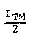 outer pair of guides and ITE for the central guide.
3. An optical guiding structure as defined in claim 1 wherein the input signal may be applied to the central guide and the predetermined length L and separation distance d are chosen so that the TE polarization is coupled into the outer pair of guides and the TM polarization emerges from the central guide, the set of output signals being defined as for said  outer pair of waveguides and ITM for the central guide.
4. An optical guiding structure as defined in claim 1 wherein the central guide and the pair of outer guides comprise optical waveguides formed in an optical substrate (15).
5. An optical guiding structure as defined in claim 4 wherein the optical substrate comprises lithium niobate and the guides comprises titanium diffused into the lithium niobate optical substrate.
6. An optical guiding structure as defined in claim 4 wherein the structure further comprises electrode means (30) disposed over each waveguide and coupled to a pair of external power sources, a first electrode (32) of said electrode means associated with the pair of outer waveguides and a second electrode (34) of said electrode means associated with the central waveguide, said electrode means when connected to said pair of external sources capable of providing increased polarization splitting between the central waveguide and the pair of outer waveguides.
7. An optical guiding structure as defined in claim 1 wherein the central guide and the pair of outer guide comprise single mode optical fiber.
Priority Applications (2)
| Application Number | Priority Date | Filing Date | Title |
|---|---|---|---|
| DE8787900767T DE3687272T2 (en) | 1986-04-14 | 1986-12-31 | OPTICAL POWER DIVIDER AND POLARIZATION DIVIDER. |
| JP87500931A JPS63503013A (en) | 1986-04-14 | 1986-12-31 | Optical power splitter and polarization splitter |
Applications Claiming Priority (2)
| Application Number | Priority Date | Filing Date | Title |
|---|---|---|---|
| US851,790 | 1986-04-14 | ||
| US06/851,790 US4772084A (en) | 1986-04-14 | 1986-04-14 | Optical power splitter and polarization splitter |
Publications (1)
| Publication Number | Publication Date |
|---|---|
| WO1987006356A1 true WO1987006356A1 (en) | 1987-10-22 |
Family
ID=25311686
Family Applications (1)
| Application Number | Title | Priority Date | Filing Date |
|---|---|---|---|
| PCT/US1986/002822 Ceased WO1987006356A1 (en) | 1986-04-14 | 1986-12-31 | Optical power splitter and polarization splitter |
Country Status (6)
| Country | Link |
|---|---|
| US (1) | US4772084A (en) |
| EP (1) | EP0262155B1 (en) |
| JP (1) | JPS63503013A (en) |
| CA (1) | CA1284908C (en) |
| DE (1) | DE3687272T2 (en) |
| WO (1) | WO1987006356A1 (en) |
Cited By (1)
| Publication number | Priority date | Publication date | Assignee | Title |
|---|---|---|---|---|
| US5491763A (en) * | 1992-04-03 | 1996-02-13 | Koninklijke Ptt Nederland N.V. | Optical hybrid with 3×3 coupling device |
Families Citing this family (27)
| Publication number | Priority date | Publication date | Assignee | Title |
|---|---|---|---|---|
| DE3741455A1 (en) * | 1987-12-08 | 1989-06-22 | Standard Elektrik Lorenz Ag | OPTICAL ISOLATOR |
| FR2626082B1 (en) * | 1988-01-14 | 1991-10-18 | Commissariat Energie Atomique | INTEGRATED OPTICAL DEVICE FOR SEPARATING POLARIZED COMPONENTS FROM A GUIDED ELECTROMAGNETIC FIELD AND METHOD FOR PRODUCING THE DEVICE |
| US4869569A (en) * | 1988-04-25 | 1989-09-26 | Bell Communications Research, Inc. | Polarizing optical waveguides |
| US5071214A (en) * | 1988-05-12 | 1991-12-10 | The Commonwealth Of Australia | Interferometric fibre optic network |
| US5008545A (en) * | 1989-10-23 | 1991-04-16 | Tektronix, Inc. | High resolution optical fault locator |
| NL9000210A (en) * | 1990-01-29 | 1991-08-16 | Nederland Ptt | INTEGRATED OPTICAL POLARIZATION SPLITTER. |
| FR2658315A1 (en) * | 1990-02-14 | 1991-08-16 | France Etat | POLARIZATION SEPARATOR FOR GUIDED LIGHT. |
| JPH04110831A (en) * | 1990-08-31 | 1992-04-13 | Nec Corp | Optical control device |
| FR2668615B1 (en) * | 1990-10-31 | 1992-12-11 | France Etat | POLARIZATION SEPARATOR FOR GUIDED LIGHT. |
| US5094526A (en) * | 1990-11-07 | 1992-03-10 | General Signal Corporation | Integrated optical waveguide doppler velocimeter |
| US5539850A (en) * | 1994-12-30 | 1996-07-23 | At&T Corp. | Polarization and wavelength independent optical waveguide tap |
| US5502781A (en) * | 1995-01-25 | 1996-03-26 | At&T Corp. | Integrated optical devices utilizing magnetostrictively, electrostrictively or photostrictively induced stress |
| US5796885A (en) * | 1996-05-09 | 1998-08-18 | Gonthier; Francois | 3×3 waveguide coupler for bidirectional dual wavelength transmission and signal sampling and method for making the same |
| IN190212B (en) * | 1996-07-23 | 2003-07-05 | Samsung Electronics Co Ltd | |
| DE19640725A1 (en) * | 1996-10-02 | 1998-04-09 | Reinhold Prof Dr Ing Noe | Network analyzer |
| GB0026415D0 (en) * | 2000-10-28 | 2000-12-13 | Bookham Technology Ltd | Polarisation beam splitters/combiners |
| US6415083B1 (en) * | 2001-03-13 | 2002-07-02 | Lockheed Martin Corporation | Traveling wave electro-optic modulator based on an organic electro-optic crystal |
| US6928215B1 (en) * | 2001-07-25 | 2005-08-09 | Lightwave Microsystems Corporation | Optical tap for optical integrated circuits |
| US7027673B1 (en) * | 2002-06-19 | 2006-04-11 | Luxtera, Inc. | Integrated dual waveguides |
| US7035491B2 (en) * | 2003-09-15 | 2006-04-25 | Little Optics, Inc. | Integrated optics polarization beam splitter using form birefringence |
| US7356206B2 (en) * | 2003-09-15 | 2008-04-08 | Infinera Corporation | Integrated optics polarization beam splitter using form birefringence |
| DE102005010805B4 (en) * | 2005-03-07 | 2010-07-22 | Schleifring Und Apparatebau Gmbh | Device for transmitting modulated optical signals generated by an optical transmitter |
| US20060228080A1 (en) * | 2005-04-08 | 2006-10-12 | Lawrence Letch | Limited combustible optical fiber |
| US7373042B2 (en) * | 2006-07-28 | 2008-05-13 | Infinera Corporation | Polarization sorter |
| GB2439136B (en) * | 2006-06-14 | 2011-02-23 | Filtronic Compound Semiconductors Ltd | A tuneable electro-optic modulator |
| US11105978B2 (en) * | 2020-02-04 | 2021-08-31 | Globalfoundries U.S. Inc. | Polarizers including stacked elements |
| CN113253384B (en) * | 2021-06-28 | 2021-10-19 | 西安奇芯光电科技有限公司 | Polarization beam splitter structure with high extinction ratio |
Family Cites Families (8)
| Publication number | Priority date | Publication date | Assignee | Title |
|---|---|---|---|---|
| US4280766A (en) * | 1977-11-21 | 1981-07-28 | The United States Of America As Represented By The Administrator Of The National Aeronautics And Space Administration | Optical gyroscope system |
| US4273444A (en) * | 1978-11-20 | 1981-06-16 | Rockwell International Corporation | Interferometer gyroscope having relaxed detector linearity requirements |
| US4299490A (en) * | 1978-12-07 | 1981-11-10 | Mcdonnell Douglas Corporation | Phase nulling optical gyro |
| JPS55103509A (en) * | 1979-02-05 | 1980-08-07 | Nippon Telegr & Teleph Corp <Ntt> | Photo coupler |
| US4390236A (en) * | 1981-03-19 | 1983-06-28 | Bell Telephone Laboratories, Incorporated | Tunable polarization independent wavelength filter |
| US4440498A (en) * | 1981-11-13 | 1984-04-03 | The United States Of America As Represented By The Secretary Of The Navy | Optical fiber gyroscope with (3×3) directional coupler |
| US4445780A (en) * | 1982-03-01 | 1984-05-01 | The United States Of America As Represented By The Secretary Of The Navy | Fiber optic rotation-sensing gyroscope with (3×2) coupler |
| US4479715A (en) * | 1982-03-09 | 1984-10-30 | Sheem Sang K | Optical rotation-sensing interferometer with (3×3)-(2×2) directional coupler |
-
1986
- 1986-04-14 US US06/851,790 patent/US4772084A/en not_active Expired - Lifetime
- 1986-12-31 DE DE8787900767T patent/DE3687272T2/en not_active Expired - Fee Related
- 1986-12-31 JP JP87500931A patent/JPS63503013A/en active Pending
- 1986-12-31 WO PCT/US1986/002822 patent/WO1987006356A1/en not_active Ceased
- 1986-12-31 EP EP87900767A patent/EP0262155B1/en not_active Expired
-
1987
- 1987-02-26 CA CA000530681A patent/CA1284908C/en not_active Expired - Lifetime
Non-Patent Citations (4)
| Title |
|---|
| Applied Physics Letters, Vol. 37, July 1980, (American Institute of Physics, New York, USA), M. MASUDA, "An Optical TE-TM mode Splitter using LINbO3 Branching Waveguide", see pages 20-21 * |
| First International Conference on Optical Fiber Sensors, 26-28 April 1983 (Institution of Electrical Engineers, London, GB), K.P. KOO et al., "Performance Characteristics of Passively Stabilized Fiber Interferometer using (3x3) Fiber Directional Couplers", pages 200-204, see figures 1-3; page 200, column 2, lines 1-63; page 201, column 1, lines 1-19 * |
| International Conference on Integrated Optics and Optical Fiber Communication, Technical Digest, 18-20 July 1977 (Institute of Electronics and Communication Engineers of Japan, Tokyo, JP), M. MINAKATA et al., "Optical Intensity Modulator using a pair of gate Couplers and Electro-Optic phase Shifters", see pages 145-148 * |
| Japanese Journal of Applied Physics, Vol. 19, Supplement 19-1, 1980 (Publication Office Japanese Journal of Applied Physics, Tokyo, JP), O. MIKAMI, "A Coupled-Waveguide TE/TM mode Splitter", see pages 455-458 * |
Cited By (1)
| Publication number | Priority date | Publication date | Assignee | Title |
|---|---|---|---|---|
| US5491763A (en) * | 1992-04-03 | 1996-02-13 | Koninklijke Ptt Nederland N.V. | Optical hybrid with 3×3 coupling device |
Also Published As
| Publication number | Publication date |
|---|---|
| EP0262155A1 (en) | 1988-04-06 |
| US4772084A (en) | 1988-09-20 |
| CA1284908C (en) | 1991-06-18 |
| DE3687272D1 (en) | 1993-01-21 |
| JPS63503013A (en) | 1988-11-02 |
| EP0262155B1 (en) | 1992-12-09 |
| DE3687272T2 (en) | 1993-04-15 |
Similar Documents
| Publication | Publication Date | Title |
|---|---|---|
| EP0262155B1 (en) | Optical power splitter and polarization splitter | |
| JP3158460B2 (en) | Polarized beam splitter for guide light | |
| CA1249155A (en) | Fiber optic polarizer with error signal feedback | |
| US5479542A (en) | All-fiber in line optical isolator | |
| US4991926A (en) | Integrated optics decorrelator | |
| US5854678A (en) | Three-axis fiber optic gyroscope having a single source and multi-coupler configuration | |
| JP7479359B2 (en) | Compact fiber optic Sagnac interferometer | |
| US5037205A (en) | Integrated optic interferometric fiber gyroscope module and method | |
| JP2724098B2 (en) | Optical wavelength filter device | |
| US4445780A (en) | Fiber optic rotation-sensing gyroscope with (3×2) coupler | |
| US5852691A (en) | Self-imaging waveguide optical polarization or wavelength splitters | |
| US5838842A (en) | Self-imaging waveguide optical polarization or wavelength splitters | |
| US4479715A (en) | Optical rotation-sensing interferometer with (3×3)-(2×2) directional coupler | |
| US5223911A (en) | Single-polarization, integrated optical components for optical gyroscopes | |
| JPH02234015A (en) | Method and system for detecting rotation of optical fiber | |
| US4904038A (en) | Guided wave optical frequency shifter | |
| CA1311546C (en) | Integrated optic interferometric fiber gyroscope module and method | |
| JPH03162617A (en) | Optical fiber resonator interferometer gyroscope | |
| JPH04259801A (en) | mach zehnder interferometer | |
| JPH0422246B2 (en) | ||
| US5311279A (en) | Integrated optical apparatus for the interferometric measurement of light waves | |
| Arditty et al. | Reciprocity properties of a branching waveguide | |
| EP0416070A1 (en) | Single-polarization, integrated optical components for optical gyroscopes. | |
| Minford et al. | Fiber optic gyroscope using an eight-component LiNbO3 integrated optic circuit | |
| JP2659787B2 (en) | Waveguide mode light selector |
Legal Events
| Date | Code | Title | Description |
|---|---|---|---|
| AK | Designated states |
Kind code of ref document: A1 Designated state(s): JP |
|
| AL | Designated countries for regional patents |
Kind code of ref document: A1 Designated state(s): AT BE CH DE FR GB IT LU NL SE |
|
| WWE | Wipo information: entry into national phase |
Ref document number: 1987900767 Country of ref document: EP |
|
| WWP | Wipo information: published in national office |
Ref document number: 1987900767 Country of ref document: EP |
|
| WWG | Wipo information: grant in national office |
Ref document number: 1987900767 Country of ref document: EP |