WO1992014180A1 - Matiere optique anisotrope, sa fabrication, dispositif a cristaux liquides dote de ladite matiere et sa production - Google Patents
Matiere optique anisotrope, sa fabrication, dispositif a cristaux liquides dote de ladite matiere et sa production Download PDFInfo
- Publication number
- WO1992014180A1 WO1992014180A1 PCT/JP1992/000097 JP9200097W WO9214180A1 WO 1992014180 A1 WO1992014180 A1 WO 1992014180A1 JP 9200097 W JP9200097 W JP 9200097W WO 9214180 A1 WO9214180 A1 WO 9214180A1
- Authority
- WO
- WIPO (PCT)
- Prior art keywords
- liquid crystal
- optically anisotropic
- crystal device
- display cell
- crystal polymer
- Prior art date
- Legal status (The legal status is an assumption and is not a legal conclusion. Google has not performed a legal analysis and makes no representation as to the accuracy of the status listed.)
- Ceased
Links
Classifications
-
- C—CHEMISTRY; METALLURGY
- C09—DYES; PAINTS; POLISHES; NATURAL RESINS; ADHESIVES; COMPOSITIONS NOT OTHERWISE PROVIDED FOR; APPLICATIONS OF MATERIALS NOT OTHERWISE PROVIDED FOR
- C09K—MATERIALS FOR MISCELLANEOUS APPLICATIONS, NOT PROVIDED FOR ELSEWHERE
- C09K19/00—Liquid crystal materials
- C09K19/04—Liquid crystal materials characterised by the chemical structure of the liquid crystal components, e.g. by a specific unit
- C09K19/38—Polymers
- C09K19/3833—Polymers with mesogenic groups in the side chain
- C09K19/3842—Polyvinyl derivatives
- C09K19/3852—Poly(meth)acrylate derivatives
- C09K19/3866—Poly(meth)acrylate derivatives containing steroid groups
-
- C—CHEMISTRY; METALLURGY
- C09—DYES; PAINTS; POLISHES; NATURAL RESINS; ADHESIVES; COMPOSITIONS NOT OTHERWISE PROVIDED FOR; APPLICATIONS OF MATERIALS NOT OTHERWISE PROVIDED FOR
- C09K—MATERIALS FOR MISCELLANEOUS APPLICATIONS, NOT PROVIDED FOR ELSEWHERE
- C09K19/00—Liquid crystal materials
- C09K19/04—Liquid crystal materials characterised by the chemical structure of the liquid crystal components, e.g. by a specific unit
- C09K19/38—Polymers
- C09K19/3833—Polymers with mesogenic groups in the side chain
- C09K19/3842—Polyvinyl derivatives
- C09K19/3852—Poly(meth)acrylate derivatives
- C09K19/3857—Poly(meth)acrylate derivatives containing at least one asymmetric carbon atom
-
- C—CHEMISTRY; METALLURGY
- C09—DYES; PAINTS; POLISHES; NATURAL RESINS; ADHESIVES; COMPOSITIONS NOT OTHERWISE PROVIDED FOR; APPLICATIONS OF MATERIALS NOT OTHERWISE PROVIDED FOR
- C09K—MATERIALS FOR MISCELLANEOUS APPLICATIONS, NOT PROVIDED FOR ELSEWHERE
- C09K19/00—Liquid crystal materials
- C09K19/04—Liquid crystal materials characterised by the chemical structure of the liquid crystal components, e.g. by a specific unit
- C09K19/40—Liquid crystal materials characterised by the chemical structure of the liquid crystal components, e.g. by a specific unit containing elements other than carbon, hydrogen, halogen, oxygen, nitrogen or sulfur, e.g. silicon, metals
- C09K19/406—Liquid crystal materials characterised by the chemical structure of the liquid crystal components, e.g. by a specific unit containing elements other than carbon, hydrogen, halogen, oxygen, nitrogen or sulfur, e.g. silicon, metals containing silicon
- C09K19/408—Polysiloxanes
-
- G—PHYSICS
- G02—OPTICS
- G02F—OPTICAL DEVICES OR ARRANGEMENTS FOR THE CONTROL OF LIGHT BY MODIFICATION OF THE OPTICAL PROPERTIES OF THE MEDIA OF THE ELEMENTS INVOLVED THEREIN; NON-LINEAR OPTICS; FREQUENCY-CHANGING OF LIGHT; OPTICAL LOGIC ELEMENTS; OPTICAL ANALOGUE/DIGITAL CONVERTERS
- G02F1/00—Devices or arrangements for the control of the intensity, colour, phase, polarisation or direction of light arriving from an independent light source, e.g. switching, gating or modulating; Non-linear optics
- G02F1/01—Devices or arrangements for the control of the intensity, colour, phase, polarisation or direction of light arriving from an independent light source, e.g. switching, gating or modulating; Non-linear optics for the control of the intensity, phase, polarisation or colour
- G02F1/13—Devices or arrangements for the control of the intensity, colour, phase, polarisation or direction of light arriving from an independent light source, e.g. switching, gating or modulating; Non-linear optics for the control of the intensity, phase, polarisation or colour based on liquid crystals, e.g. single liquid crystal display cells
- G02F1/133—Constructional arrangements; Operation of liquid crystal cells; Circuit arrangements
- G02F1/1333—Constructional arrangements; Manufacturing methods
- G02F1/1335—Structural association of cells with optical devices, e.g. polarisers or reflectors
- G02F1/13363—Birefringent elements, e.g. for optical compensation
- G02F1/133636—Birefringent elements, e.g. for optical compensation with twisted orientation, e.g. comprising helically oriented LC-molecules or a plurality of twisted birefringent sublayers
Definitions
- the present invention relates to an optically anisotropic material, a method of manufacturing an optically anisotropic material, and a method of manufacturing a liquid crystal device having an optically anisotropic material and a liquid crystal device S having an optically anisotropic material.
- the present invention relates to a liquid crystal device, and more particularly to a liquid crystal device that realizes black and white display.
- Fig. 31 shows the optical characteristics of the conventional STN liquid crystal device S in the OFF state.
- reference numeral 61 denotes incident light.
- 61 is natural light, includes light of all wavelengths in the visible region, and has a random polarization direction.
- the polarization direction becomes a set of linearly polarized light 62, 63, 64, and the like.
- 62, 63, and 64 indicate polarizations of wavelengths of 450 nm, 550 nm, and 650 nm, respectively.
- the linearly polarized light such as 62, 63, 64
- the liquid crystal element 7 in the display cell 55 has a twisted structure of a nematic liquid crystal exhibiting optically uniaxial refractive index anisotropy. Liquid crystal with such a structure
- the polarization state changes.
- the results under the conditions of the conventional STN liquid crystal device whose spectrum is shown in Fig. 32, are shown as polarization states such as 65, 66, and 67, respectively. It becomes.
- polarization states 65, 66, and 67 are shown as polarization states.
- Fig. 30 shows a two-layer super twisted nematic liquid crystal device capable of monochrome display, (B) and (C) film-compensated liquid crystal devices. It is. As shown in (A), (B) and (C) of FIG. 30, these liquid crystal devices capable of displaying black and white include a polarizing plate 8 and an optically anisotropic member 54 and And display cell 55 as its constituent element.
- the display cell is an STN liquid crystal cell.
- STN liquid crystal cells have a twist angle of the liquid crystal. It is as large as 200 degrees to 240 degrees and has a steep threshold, which is applied to increase the capacity of a simple matrix liquid crystal device.
- this color compensator When this color compensator is manufactured from liquid crystal cells, it is heavy, thick, and expensive to manufacture because two glass substrates are used as supplementary cells. There are issues to be solved.
- a uniaxially stretched film as shown in (B) has been put into practical use as a substitute for this color supplement cell.
- the original purpose is not sufficient as a color compensation for the displayed cell.
- the coloring due to the birefringence of the liquid crystal display cell is almost complemented, but the coloring effect due to the optical rotation remains, so that a complete black-and-white display is achieved. It cannot be obtained, and it is difficult to colorize. Another problem is that the viewing angle is narrow.
- the optical anisotropic body, the liquid crystal device having the optical anisotropic body, and the method for manufacturing a liquid crystal device according to the present invention greatly improve the viewing angle and contrast of a conventional liquid crystal device,
- An object of the present invention is to provide a liquid crystal device that simplifies the manufacturing process or that is lightweight, thin, and low in cost.
- the optically anisotropic body of the present invention has at least a transparent substrate and at least one more siloxane or acryl or methacryl chain in the skeleton.
- the liquid crystal polymer of the present invention is twist-oriented having a helical axis in a uniaxial direction or a direction normal to the substrate, and has a glass transition temperature at room temperature or higher. It is characterized by showing a nematic phase or a twisted nematic phase.
- the optical anisotropic body of the present invention has at least a transparent substrate and at least one more siloxane or acrylyl or methacrylyl skeleton.
- the mixture of the liquid crystal polymer and the low molecular weight optically active compound of the present invention is composed of a mixture of the liquid crystal polymer and the low molecular weight optically active compound in the uniaxial direction or the substrate normal direction. Twisted orientation with helical axis, glass at room temperature or higher It is characterized by having a transition temperature and showing a nematic phase or a twisted nematic phase.
- the optically anisotropic body of the present invention comprises at least a transparent substrate and at least one layer of siloxane or acryl chains or a clear chain.
- the mixture of the liquid crystal polymer and the optically active polymer of the present invention has a twisted orientation having a helical axis in the direction normal to the substrate, and has a glass transition temperature above room temperature. It has a feature of indicating a nematic phase or a twisted nematic phase.
- the liquid crystal device provided with the optical anisotropic body of the present invention includes at least one pair of polarizing plates, a liquid crystal display cell, a transparent substrate, and at least one layer of siloxane. It consists of an optically anisotropic body containing a liquid crystalline polymer having a skeleton of an acrylic chain or a methacrylic chain or a methacrylic chain, and these are disposed between the polarizing plates. It is characterized by being pinched.
- the liquid crystal device provided with the optically anisotropic body of the present invention comprises at least one pair of polarizing plates, at least one liquid crystal display cell, and at least one layer of a siloxane chain.
- At least a liquid crystal device equipped with the optical anisotropic body of the present invention is provided.
- a pair of polarizers, a liquid crystal display cell and at least one layer of white It is composed of an optically anisotropic body containing a liquid crystal polymer having a skeleton of a xan chain, a acrylyl chain, or a methacryl chain, and contains the liquid crystal polymer. It is characterized in that the anisotropic body is in contact with the liquid crystal display cell.
- the process for the production of an optically anisotropic body according to the invention is characterized in that at least a siloxane or a acryl chain or a methacryl group is provided on at least a transparent substrate.
- the method of manufacturing a liquid crystal device having an optically anisotropic body includes a step of performing a directing process on at least a surface of the liquid crystal display cell that is not in contact with the liquid crystal, and at least a further step of A step of forming a material containing a liquid crystal polymer having a siloxane chain, an acrylyl chain or a methacryl chain in a skeleton; and thereafter, heating the material containing the liquid crystal polymer. And a step of rushing.
- the liquid crystal device having the optically anisotropic material and the method for manufacturing the liquid crystal device having the optically anisotropic material according to the present invention may include: a polarization axis direction of the polarizing plate; and a molecular long axis of the liquid crystal polymer adjacent thereto. It is characterized in that the angle between the direction and the direction is from 30 degrees to 60 degrees.
- the value of A nxd of the nematic layer of the liquid crystal display cell is 0.5.
- the feature is that the power is 1.
- the liquid crystal device provided with the optically anisotropic material and the method of manufacturing the liquid crystal device provided with the optically anisotropic material of the present invention have a twist angle of the liquid crystal polymer layer included in the optically anisotropic material of one. It is characterized by the fact that it is 300 degrees from 550 degrees.
- the liquid crystal device provided with the optically anisotropic material and the method for manufacturing the liquid crystal device provided with the optically anisotropic material according to the present invention can be formed by a method of manufacturing a liquid crystal polymer layer contained in the optically anisotropic material.
- the feature is that the power is 0.2 yum and 1.8 yum.
- the liquid crystal device having the optical anisotropic body and the method of manufacturing the liquid crystal device having the optical anisotropic body according to the present invention are included in the nematic liquid crystal of the liquid crystal display cell and the optical anisotropic body.
- the orientation direction of liquid crystal molecules on the surface facing the liquid crystal polymer layer is approximately 90 degrees.
- the liquid crystal device having the optical anisotropic body and the method of manufacturing the liquid crystal device having the optical anisotropic body according to the present invention are described in the nematic phase in which the liquid crystal layer of the liquid crystal display cell is oriented. Or the cholesteric phase,
- the method of manufacturing a liquid crystal device having an optically anisotropic material and a method of manufacturing a liquid crystal device having an optically anisotropic material include a twist direction of a polymer phase included in the optical anisotropic material and a liquid crystal display.
- the nematic liquid crystal of the cell is characterized in that the twist direction of the liquid crystal is reversed.
- the liquid crystal device provided with the optically anisotropic material and the method of manufacturing the liquid crystal device provided with the optically anisotropic material according to the present invention include a liquid crystal polymer layer and a liquid crystal display cell included in the optically anisotropic material. It is characterized in that the twist angle of the liquid crystal and the film n X d are almost equal.
- the optically anisotropic transparent substrate of the present invention most preferably has no optical anisotropy due to the effect of the optical anisotropy.
- an amorphous high molecular film obtained by a glass / cast method ⁇ an optically anisotropic material obtained by a stretching method and a material having a positive optical anisotropy.
- a film in which materials with negative optical anisotropy are superimposed, or a film obtained by stretching a mixture of a material with positive optical anisotropy and a material with negative optical anisotropy Films are particularly desirable.
- an optimum material can be selected in consideration of the solvent resistance, heat resistance, and the like of the substrate to be coated.
- polyimide not only polyimide, but any other liquid crystal material alignment agent can be used. Its curing temperature is not limited.
- an ordinary multi-plex driving method can be used.
- the alignment method of the present invention it is preferable to directly rub the liquid crystal cell or rub it on an alignment agent.
- the phase transition series of the liquid crystal polymer of the present invention be transformed into a glass state, a nematic phase, and an isotropic liquid phase with an increase in temperature.
- the glass transition temperature is higher than the upper limit of the operating temperature range of the liquid crystal device, and the transition temperature from the nematic phase to the isotropic liquid phase is obtained. Is 100. It should be between C and 150 ° C.
- the liquid crystal polymer of the present invention has an acrylic chain or Side chain type liquid crystal polymer having a mono-chain, that is, a mesogen group is skeletoned through a spacer of an ethylene chain having at least one carbon atom.
- the molecular structure of a liquid crystal polymer exhibiting a nematic phase bonded to the polymer is not limited to the examples.
- the temperature at which the liquid crystal polymer of the present invention is oriented is desirably set at a temperature close to the transition temperature of the nematic-isotropic liquid phase of the liquid crystal high molecule. .
- C force i et al 250.
- C is Nozomu or Shi Rere is further to Nozomu or to rather is Ru 8 0 ° C or al 1 3 0 e C der.
- the cooling rate at the time of cooling to room temperature after the orientation of the liquid crystal polymer of the present invention is faster, it is not particularly limited to the examples.
- the force applied to the liquid crystal polymer of the present invention may be, for example, an R-shaped twisted right-handed liquid crystal display cell if the liquid crystal display cell is a counterclockwise liquid crystal cell.
- the present invention is not limited to this example as long as the cell for display is an optically active compound containing an asymmetric carbon, such as an S-isomer such that the cell is clockwise and twists to the left. No. Empirically, there is no particular problem in the use of a compound that turns to the left and turns to the right .. Even for compounds containing irregular carbon, the twist direction depends on the temperature. Or, if you do not know the twisting direction of each d-body and one body, you can use after checking the twisting direction of the mo.
- the capillary pallets are not limited to low molecular weight compounds, and even if they are polymerized, the present invention can be applied. It doesn't hurt your advantage. That is, irregular carbon is included in the skeleton of the liquid crystal polymer that can be used in the present invention. In the case where a site having an element is provided, or in a process of synthesizing a liquid crystal polymer that can be used in the present invention, a monomer containing an asymmetric carbon in advance is used.
- the copolymer is prepared and copolymerized, if the copolymer shows a chiral nematic phase, the copolymer is also considered to be a capillary donut. Can be used. Or, by adjusting the direction and angle of the screw, the copolymer alone can be used.
- a roll coating method, printing, a spin coating method, a method using a bar coating method, and the like are desired. Better than that. A uniform thickness can be secured, and the present invention is not limited to this embodiment. Casting from a solvent, diving, and the like can also be used.
- the liquid crystal device of the present invention includes at least a liquid crystal cell, a polarizing plate, and the optically anisotropic body of the present invention as constituent elements.
- the polarization axis, the rubbing direction of the liquid crystal cell, and the molecular axis direction of the liquid crystal polymer are not limited to the present embodiment.
- a color filter for preventing light leakage between the electrodes, Alternatively, a lens or the like for improving the efficiency of the transmitted light of the liquid crystal cell can be provided.
- the rubbing method of the present embodiment is not limited to the embodiment. That is, in the present embodiment, any material that is usually used for the orientation of liquid crystal molecules, such as nylon brush, cotton, and velsed, can be used. Also, the fixed rubbing method is good.
- liquid crystal polymer which is an optically anisotropic material
- the polarizing plate can be directly attached on the optically anisotropic body.
- the liquid crystal device of the present invention may have an optically anisotropic surface facing the liquid crystal cell or be directly in contact with the liquid crystal cell via a spacer. It is permissible to adopt a configuration that does not require a connection.
- the liquid crystal device of the present invention may be configured such that the polarizing plate does not directly contact a liquid crystal high molecule, which is an optically anisotropic substance, through a spacer. ,
- the polymer material having liquid crystallinity according to the invention is 60. 1 to 5 from c
- c has a transition temperature to an isotropic liquid phase, and can be oriented at a low temperature around 60 "C to 150.c.
- the polymer material having liquid crystallinity of the present invention is: Specifically, a compound having a mesogen group in the side chain is desirable, and more preferably a siloxane compound having a mesogen group in the side chain.
- the molecular weight of the molybdenum is preferably in the range of 150 to 2000, more preferably in the range of 150 to 2000.
- the liquid-day rii molecules used for the optically anisotropic material of the present invention desirably have a nematic phase of 7J ⁇ 3.
- the polymer exhibiting liquid crystallinity of the present invention If the material does not require the twist orientation, a liquid crystalline polymer material showing a nematic phase can be used alone.
- Light that requires orientation In its tail anisotropic element. Shows the Collector scan te-click phase when the light Gakukatsu of a reduction compounds that Yusuke in the backbone Material is desired.
- the liquid crystalline polymer of the present invention is prepared by adding a chiral dopant to an ordinary liquid crystal material having an optically active compound in the skeleton or a polymer material having an optically active site in the skeleton. Can be used. In addition, a polymer material having an optically active site can be used alone in order to obtain a twist orientation. In Examples 1 to 43, similar effects can be obtained by using not only the polymer compound having liquid crystallinity but also the following compounds. Select at least one of the following compounds (1) to (34) or a polymer, or use a mixture of two or more of them. You can do things.
- the compound or polymer having an optically active site is shown in the following (35). (55) can be used. N0 ⁇ g) -OO0 ⁇ g> -02H0HpsH20 S) ⁇ 10 £ H0
- FIG. 33 is an explanatory diagram of the optical characteristics of the liquid crystal device of the present invention in the OFF state. Comparing Fig. 31 and Fig. 33, Fig. 33 shows that Fig. 31 shows that the component contains an optically anisotropic material consisting of a liquid crystal polymer film. They are different. In order to simplify the explanation, the conditions of the components excluding the optical anisotropic body 54 and the polarizing plate 8 are the same as those of the conventional STN liquid crystal device shown in FIG.
- the polarization states 75, 76, 77 of each wavelength after passing through the display cell 55 are the same as those of FIG. They are exactly the same.
- the polarized light 75, 76, 77 next passes through the optically anisotropic body 54 in the case of FIG.
- the optical anisotropic body 54 can cancel the wavelength dispersion generated by the polarization 75, 76, 77 passing through the display cell 55. This has the effect of reducing Therefore, the polarized lights 75, 76, and 77 pass through the optically anisotropic body, and return to linear false lights such as 78, 79, and 80, respectively.
- FIG. 7 shows the spectrum of the emitted light at this time.
- the coloring phenomenon in the 0 FF state can be eliminated.
- ⁇ N according to many experimental results and computer simulations according to the examples described later, under various conditions. Check that there is no coloring.
- the condition at this time is (1) The values of nd of the display cell and ⁇ d of the optically anisotropic body are almost equal.
- the coloring phenomenon can be eliminated as described above.
- the optical supplement of the two-layer super-stable nematic liquid crystal cell disclosed in detail in Japanese Patent Publication No. 38,146 Although the details are omitted because they are the same as the effect, in the liquid crystal device obtained in this way, a straight line light that has passed through a pair of polarizing plates at a time is used. Since the display cell and the color compensator pass through at least two layers "" 3, the coloration due to the birefringence and optical rotation of the STN display cell is eliminated, and the color of the STN display cell is reduced from about 400 nm to 7 nm.
- the light In the wavelength range of 100 nm, the light becomes almost elliptical light in the major axis direction. Therefore, when passing through one of the polarizing plates, a specific wavelength range is obtained. The light is not blocked, and as a result, the light after passing through the polarizer has a color close to white.
- the present invention relates to a method for manufacturing the optical anisotropic body and the optical cuboid of the present invention, a liquid crystal device provided with the optical anisotropic body, and a method for manufacturing a liquid crystal device provided with the optical anisotropic body.
- a display device such as a conventional two-layer type super nematic liquid crystal device can be made compact and thin without impairing the display characteristics such as the contrast and the viewing angle.
- Liquid says Equipment can be provided at low cost.
- FIG. 1 is a schematic cross-sectional view of an example of an optically anisotropic body according to Embodiment 1 of the present invention
- FIG. 2 is a schematic cross-sectional view of an example of an optically anisotropic body according to Embodiment 2 of the present invention
- FIG. 3 is a schematic cross-sectional view of an example of the optically anisotropic body according to the third embodiment of the present invention
- FIG. 4 is a schematic cross-sectional view of an example of the optically anisotropic body according to the fourth embodiment of the present invention.
- FIG. 5 is a schematic cross-sectional view of an example of a liquid crystal device provided with the optically anisotropic member obtained in Example 1 of the present invention.
- FIG. 1 is a schematic cross-sectional view of an example of an optically anisotropic body according to Embodiment 1 of the present invention
- FIG. 2 is a schematic cross-sectional view of an example of an optically anisotropic body according to Embodiment
- FIG. 6 is a diagram showing the direction of orientation of the liquid crystal, the direction of the absorption axis of the light source plate, and the direction of the molecular long axis of the liquid crystal polymer.
- FIG. 7 is a diagram showing a contrast curve of the liquid crystal device of the present invention.
- FIG. 8 is a schematic cross-sectional view of an example of a liquid crystal device provided with the optically anisotropic material obtained in Example 2 of the present invention
- FIG. 9 is an optically anisotropic material obtained in Example 3 of the present invention.
- FIG. 10 is a schematic cross-sectional view of an example of a liquid crystal device provided with: FIG.
- FIG. 10 is a schematic cross-sectional view of an example of a liquid crystal device provided with the optically anisotropic member obtained in Embodiment 4 of the present invention.
- 19 is a schematic cross-sectional view of an example of a liquid crystal device including an optically anisotropic member according to a ninth embodiment of the present invention.
- FIG. 12 is a schematic cross-sectional view of one example of a liquid crystal device provided with the optically anisotropic member of Example 10 of the present invention.
- FIG. 13 is a liquid crystal provided with the optically anisotropic member of Example 11 of the present invention.
- FIG. 14 is a schematic cross-sectional view of an example of the device, and FIG.
- FIG. 14 is a schematic cross-sectional view of an example of a liquid crystal device including the optically anisotropic member of Example 12 of the present invention.
- FIG. 15 shows an example of a method for manufacturing an optically anisotropic member according to the first embodiment of the present invention.
- FIG. 16 is a view showing an example of a method for producing an optically anisotropic body according to the second embodiment of the present invention, and
- FIG. 17 is a view showing an optically anisotropic body according to the third embodiment of the present invention.
- FIG. 3 is a view showing an example of a manufacturing method.
- FIG. 18 shows an example of a method for producing an optically anisotropic material according to Example 4 of the present invention, and FIG.
- FIG. 19 shows an example of a method for producing an optically anisotropic material according to Example 18 of the present invention.
- FIG. 20 is a diagram showing an example of a method for manufacturing the optically anisotropic material of Example 19 of the present invention.
- FIG. 21 is a diagram showing an optically anisotropic material of Example 25 of the present invention.
- 5 is a schematic view of an example of a method for manufacturing a liquid crystal apparatus provided.
- FIG. 22 is a schematic view of an example of a method for manufacturing a liquid crystal device provided with the optically anisotropic member of Example 31 of the present invention, and
- FIG. 23 is an optically anisotropic member of Example 32 of the present invention.
- FIG. 24 is a schematic view of an example of a method of manufacturing a liquid crystal device having a liquid crystal device
- FIG. 24 is a schematic view of an example of a method of manufacturing a liquid crystal device having an optically anisotropic member of Example 33 of the present invention
- FIG. 15 is a schematic view of an example of a method for manufacturing a liquid crystal device including the optically anisotropic member according to Example 34 of the present invention
- FIG. 26 is a schematic view of an example of a method for manufacturing a liquid crystal device provided with the optically anisotropic member of Example 35 of the present invention
- FIG. 27 is provided with the optically anisotropic member of Example 36 of the present invention.
- FIG. 28 is a schematic view of an example of a method of manufacturing a liquid crystal device
- FIG. 28 is a schematic view of an example of a method of manufacturing a liquid crystal device having an optically anisotropic member according to Example 37 of the present invention.
- FIG. 13 is a schematic view of an example of a method for manufacturing a liquid crystal device provided with the optically anisotropic member of Example 38.
- FIG. 30 is a schematic cross-sectional view of a conventional black-and-white display liquid crystal device, and FIG. 31 is an explanatory diagram of an OFF-state optical characteristic of the conventional STN liquid crystal device.
- Fig. 32 is a diagram showing the spectrum of a conventional STN liquid crystal device. is there.
- FIG. 33 is an explanatory diagram of the optical characteristics of the liquid crystal device of the present invention in the OFF state.
- FIG. 34 shows the viewing angle and contrast of a conventional three-crystal liquid crystal device.
- FIG. 35 shows the viewing angle and contrast of the liquid crystal device of the present invention. This is the figure.
- FIG. 36 is a diagram showing an example of a desired range of the liquid crystal display cell and the optically anisotropic member in the embodiment of the present invention
- FIG. 37 is a diagram showing the embodiment of the present invention.
- FIG. 38 shows an example of a desirable range of the liquid crystal display cell and the optically anisotropic body
- FIG. 38 is a view of the liquid crystal display cell and the optically anisotropic body in the embodiment of the present invention.
- FIG. 3 is a diagram showing an example of a desired range
- FIG. 3 is a diagram showing an example of a desired range of a liquid crystal display cell and an optically anisotropic member in the embodiment of the present invention.
- the figure shows an example of the desired range of the liquid crystal display cell and the optically anisotropic element in the embodiment of the present invention.
- FIG. 41 shows the liquid crystal display in the embodiment of the present invention.
- FIG. 4 is a diagram showing an example of a desired range of a cell and an optically anisotropic body.
- FIG. 1 shows a schematic cross-sectional view of an example of the optically anisotropic body of the present invention.
- a polyimide thin film 2 (SP740, manufactured by Toray Industries, Inc.) is formed on a transparent substrate 1, and the polyimide thin film 2 on this substrate 1 is uniaxially laminated. Bing processing is done and it is ready.
- the liquid crystal polymer film 3 is twist-oriented at 230 degrees clockwise in the twisting direction.
- the optically anisotropic body of the present invention has the effect of compensating the coloring of the STN liquid crystal cell due to the optical rotation and birefringence due to the twist of the liquid crystal, and the high cost of the liquid crystal device. It was possible to achieve a high level of contrast and a high field of view.
- FIG. 2 shows a schematic view of a cross section of an example of the optical variant of the present invention.
- a rubbing process is performed in one axis direction.
- this transparent substrate about 6 m of side chain type liquid crystal molecules (3) exhibiting a nematic phase having the siloxane chains shown in the skeleton (3) and (2 ) Of 95%: 5% mixture, and 5% of optically active compound having an asymmetric center, CB-15 (37), manufactured by Merck & Co., Ltd.
- the liquid crystal high molecular film 3 in which ⁇ is formed is twist-oriented at 230 degrees clockwise in the twisting direction.
- the optically anisotropic material of the present invention has the effect of compensating for the coloring of the STN liquid crystal cell due to the optical rotation and birefringence due to the twisting of the liquid crystal of the liquid crystal. Contrast and high viewing angle were realized.
- Example 3 Abbreviation of cross section of an example of the optically anisotropic body of the present invention
- the figure is shown in Fig. 3.
- a polyimide thin film 2 (SP740, manufactured by Toray Industries, Inc.) is formed on a transparent substrate 1, and the polyimide thin film 2 on this substrate 1 is uniaxially laminated. The bin is being processed.
- a side-chain liquid crystal polymer (about 6> um) exhibiting a nematic phase having the siloxane chain shown above in its skeleton ( 95% of 3) and (2): Liquid crystal height with addition of 5% of CB-15 (37), an optically active compound having an asymmetric center in the mixture of 5% Molecular film 3 is formed.
- the optically anisotropic body of the present invention has the effect of compensating for the coloring of the STN liquid crystal cell due to the optical rotation and birefringence due to the twist of the liquid crystal, and has a high content of the liquid crystal device. It was possible to achieve a lasting and high field of view.
- FIG. 4 shows a schematic diagram of a cross section of an example of the optically anisotropic body of the present invention.
- a rubbing treatment is performed in a uniaxial direction.
- this transparent substrate about 6 m of the side-chain type liquid crystal polymer (3) and (2) exhibiting a nematic phase having the siloxane chain shown in the skeleton above.
- 95% of the liquid crystal polymer film which is a mixture of 5% and 5% of an optically active compound having an asymmetric center, CB-15 (37), manufactured by Merck & Co., Ltd. 3 is formed.
- a transparent protective film 4 having no optical anisotropy is formed.
- this liquid crystal polymer film 3 Twisted at 230 degrees clockwise.
- the optical anisotropic body of the present invention has an effect of compensating for the coloring of the STN liquid crystal cell due to the optical rotation and the birefringence due to the twist of the liquid crystal, and the liquid crystal device has an effect. High contrast and a wide viewing angle were achieved.
- FIG. 5 shows a schematic cross-sectional view of an example of the liquid crystal device of the present invention provided with the optically anisotropic material obtained in Example 1.
- the transparent electrode 51 and the transparent substrate 5 of the liquid crystal cell having the liquid crystal directing film 52 are adhered via the spacer 6, and the liquid crystal is interposed therebetween.
- (LI 45506 manufactured by Merck & Co.) 7 is vacuum-injected.
- the optical anisotropic body and the liquid crystal cell are provided between two polarizing plates 8.
- FIG. 6 shows the orientation direction of the liquid crystal, the direction of the absorption axis of the polarizing plate, and the direction of the molecular long axis of the liquid crystal molecule at that time.
- FIG. 6 shows the orientation direction of the liquid crystal, the direction of the absorption axis of the polarizing plate, and the direction of the molecular long axis of the liquid crystal molecule at that time.
- reference numeral 9 denotes the rubbing direction of the lower% plate of the liquid crystal display cell in FIG. 5
- reference numeral 10 denotes the upper electrode substrate of the liquid crystal display cell in FIG. 11 is the long axis direction of the liquid crystal molecules adjacent to the liquid crystal display cell of the liquid crystal polymer film 3 in FIG. 5, and 12 is the liquid crystal in FIG.
- the direction of the long axis of the liquid crystal molecules adjacent to the upper polarizing plate 8 of the polymer film 3, 13 is the direction of the polarizing axis (absorption axis) of the lower polarizing plate 8 in FIG. .
- the direction of the polarization axis (absorption axis) of the upper polarizer 8 you only that in FIG. 5, 1 to 5 liquid that you only in FIG.
- Fig. 7 shows the contrast curve at that time.
- Fig. 34 (D), (E), and (F) denote the conventional two-layer super parts istone, respectively. It shows the relationship between the contrast and viewing angle of a liquid crystal device using a single-axis stretched film and a liquid crystal device using two uniaxially stretched films. are doing.
- FIG. 35 shows the relationship between the contrast and the viewing angle of the liquid crystal device provided with the optically anisotropic member formed in this example. Obviously, a liquid crystal device with improved viewing angle characteristics was obtained.
- FIG. 8 is a schematic cross-sectional view of an example of a liquid crystal device using the optically anisotropic body of Embodiment 2.
- a transparent substrate 51 of a liquid crystal cell having a transparent electrode 51 and a liquid crystal orientation film 52 is attached via a spacer 6.
- a liquid crystal (ZL14506, manufactured by Merck & Co.) 7 is vacuum-injected between them.
- the optical anisotropic body and the liquid crystal display cell are provided between two polarizing plates 8. Since the configuration other than the following is the same as that of the fifth embodiment, in this embodiment, the above conditions are set as follows. Angle 16 is 85 degrees and angle 17 is 45 degrees.
- the twist angle 15 of the liquid crystal display cell is left twisted by about 200 degrees, and the ⁇ d of the liquid crystal 7 in the liquid crystal display cell is 0.85 yum.
- FIG. 9 shows a schematic cross-sectional view of an example of a liquid crystal device using the optically anisotropic body of Embodiment 3.
- a transparent substrate 51 of a liquid crystal cell having a transparent electrode 51 and a liquid crystal alignment film 52 is adhered via a spacer 6, and a liquid crystal ( ZLI4506) 7 manufactured by Merck is vacuum-injected.
- the optical anisotropic body and the liquid crystal display cell are provided between two polarizing plates 8.
- the orientation of the liquid crystal at that time, the direction of the absorption axis of the polarizing plate, and the direction of the molecular long axis of the liquid crystal polymer were the same as in Example 5.
- Angle 16 is 80 degrees and angle 17 is 50 degrees.
- the twist angle 15 of the liquid crystal display cell is twisted to the left by about 230 degrees, and the liquid crystal 7 in the liquid crystal display cell is twisted.
- ⁇ nxd is 0.85 ym.
- FIG. 10 shows a schematic cross-sectional view of an example of a liquid crystal device using the optically anisotropic material of Example 4.
- a transparent electrode 51 and a liquid crystal cell transparent substrate 5 having a liquid crystal alignment film 52 are adhered via a spacer 6 between them.
- Liquid crystal (ZLI4506 manufactured by Merck) 7 is vacuum-injected.
- the optical anisotropic body and the liquid crystal display cell are provided between two polarizing plates 8.
- the alignment direction of the liquid crystal, the direction of the absorption axis of the polarizing plate, and the direction of the molecular long axis of the liquid crystal polymer were the same as in Example 5.
- the above conditions are set as follows. Angle 16 is 90 degrees and angle 17 is 45.
- Fig. 11 shows a schematic cross-sectional view of one example of the liquid crystal device of the present invention.
- a transparent substrate 5 of a liquid crystal cell having a transparent electrode 51 and a liquid crystal orientation film 52 is a spacer.
- the liquid (ZLI4506 manufactured by Merck) is vacuum-injected between them.
- a polyimide thin film 2 (S ⁇ 740, manufactured by Toray Industries, Inc.) is formed on the transparent substrate 5 of the liquid crystal cell not in contact with the liquid crystal of the liquid crystal display cell.
- the polyimide thin film 2 on the transparent substrate 5 is subjected to a rubbing treatment in the -axis direction.
- a side-chain type liquid crystal height of about 6 / m2 which has a nematic phase having the above-mentioned oxa xan chain in the skeleton, is shown.
- the added liquid crystal polymer film 3 is formed.
- the liquid crystal fe molecular film 3 is twisted in the twisting direction clockwise at 230 degrees.
- a liquid crystal display cell having an optically anisotropic body is provided between the two light emitting plates 8.
- the direction of the liquid crystal, the direction of the absorption axis of the polarizing plate, and the direction of the long axis of the liquid crystal polymer were the same as in Example 5.
- the above conditions were used as follows. are doing.
- the angle 15 is 89 degrees
- the angle 17 is 45 degrees
- the twist angle 15 of the liquid crystal display cell is about 200 degrees left twist.
- ⁇ n Xd of liquid crystal 7 in the display cell is 0.85 ym. Then, the driver for driving the liquid crystal and the circuit for driving the liquid crystal were brought into contact with the liquid crystal cell. The light source for lighting was installed behind the liquid crystal cell, and the liquid crystal device was assembled. When a voltage corresponding to the ON / OFF voltage was applied to the liquid crystal device, black-and-white display was confirmed, and the same display characteristics as in Example 5 were obtained.
- FIG. 12 is a schematic cross-sectional view of an example of the liquid crystal device of the present invention.
- a transparent substrate 5 of a liquid crystal display cell having a transparent electrode 51 and a liquid crystal alignment film 52 is adhered via a spacer 6 and a liquid crystal is interposed between the substrates.
- (ZLI 4506 manufactured by Merck) 7 is vacuum-injected.
- a rubbing treatment is performed in a uniaxial direction.
- a liquid crystal polymer film 3 is formed by adding 5% of Merck's CB-15 (37), an optically active compound having an asymmetric center, to a 10% mixture. It has been done.
- the liquid crystal polymer film 3 is twist-oriented at 230 degrees clockwise in the twisting direction.
- the liquid crystal display cell provided with the present optical anisotropic body is provided between two polarizing plates 8. The orientation of the liquid crystal at that time, the direction of the absorption axis of the polarizing plate, and the direction of the molecular long axis of the liquid crystal polymer were the same as in Example 5.
- the above conditions are set as follows. Angle 16 is 85 degrees and angle 17 is 45 degrees.
- the twist angle 15 of the liquid crystal display cell is twisted to the left by about 230 degrees, and the ⁇ n Xd force of the liquid crystal 7 in the liquid crystal display cell ⁇ 0.85 m.
- a liquid crystal driving driver and a liquid crystal driving circuit were connected to the above liquid crystal cell, and a light source for illumination was installed behind the liquid crystal cell to assemble the liquid crystal device.
- a voltage corresponding to the ON, OFF voltage was applied to this liquid crystal device, a monochrome display was confirmed, and the same display characteristics as in Example 5 were obtained.
- FIG. 13 shows a schematic cross-sectional view of one example of the liquid crystal device of the present invention.
- a transparent substrate 5 of a liquid crystal cell having a transparent electrode 51 and a liquid crystal alignment film 52 is adhered via a spacer 6.
- a liquid crystal (ZLI4506 manufactured by Merck) 7 is vacuum-injected.
- a polyimide thin film 2 SP740, manufactured by Toray Industries, Inc.
- the polyimide thin film 2 on the transparent substrate 5 is subjected to a uniaxial rubbing treatment.
- this polyimide thin film 2 about 6 m of a side chain type liquid crystal polymer exhibiting a nematic phase having the siloxane moiety shown above in its skeleton.
- the liquid crystal polymer film 3 is formed. Further, a protective film 4 having no optical anisotropy is formed on the liquid crystal polymer film 3. On the other hand, the liquid crystal polymer film 3 is twisted in a twisting direction at 230 degrees to the right in the twisting direction.
- the liquid crystal display cell equipped with this optically anisotropic material has two polarizing plates S It is installed between. At that time, the orientation of the liquid crystal, the direction of the absorption axis of the polarizing plate, and the direction of the molecular long axis of the liquid crystal polymer were in accordance with Example o. Has been set.
- Angle 16 is 100 degrees
- angle 17 is 45 degrees
- the twist angle 15 of the liquid B B H display cell is twisted about 200 degrees to the left.
- the ⁇ Xd of the liquid crystal 7 in the day-to-day cell is 0,85 m.
- FIG. 14 is a schematic cross-sectional view of an example of the liquid crystal device of the present invention.
- a transparent electrode 51 and a transparent substrate 5 of a liquid crystal cell having a liquid crystal alignment film 52 are adhered via a spacer 16 between them.
- Liquid crystal (ZLI4506 manufactured by Merck & Co.) 7 is vacuum-injected.
- a uniaxial rubbing process is performed on the transparent substrate 5 of this liquid crystal display cell.
- Liquid crystal polymer film 3 is formed. Furthermore, a protective film 4 having no optical anisotropy is formed on the liquid crystal polymer film 3. On the other hand, the liquid crystal polymer film 3 is twisted at 230 degrees in the twisting direction clockwise.
- a liquid crystal display cell provided with the present optical anisotropic body is provided between two polarizing plates 8. At this time, the orientation of the liquid crystal, the direction of the absorption axis of the polarizing plate, and the direction of the long axis of the liquid crystal polymer were the same as in Example 5.
- the above conditions are set as follows. Angle 16 is 90 degrees and angle 17 is 45 degrees.
- the twist angle 15 of the liquid crystal display cell is twisted to the left by about 200 degrees, and the nxd of the liquid crystal 7 in the liquid crystal display cell is 0.85> m.
- the driver for driving the liquid crystal and the circuit for driving the liquid crystal were connected to the liquid crystal cell, and the light source for illumination was installed behind the liquid crystal cell to assemble the liquid crystal device.
- a voltage corresponding to the ON / OFF voltage was applied to the liquid crystal device, monochrome display was confirmed, and the same display characteristics as in Example 5 were obtained.
- the polarizing plate 8 is made of a surface of the liquid crystal polymer film 3 or a protective film 4 on the liquid crystal polymer film 3 and an organic material. Similar optical characteristics were obtained in a liquid crystal device that was optically adhered through an adhesive.
- FIG. 15 shows an example of a method for producing the optically anisotropic material of Example 1 of the present invention.
- Poly on transparent substrate 1 A 5F SP740, manufactured by Toray Industries, Inc.
- the poly-slot-thin film 2 on this substrate is subjected to one-way rotational rubbing using nylon brushes 20, and the siloxane chains shown earlier are used as a skeleton.
- FIG. 16 shows an example of a method for producing the optically anisotropic material of Example 2 of the present invention.
- Rotational rubbing is performed in one direction using a nylon brush 20 on the transparent substrate 1, and the nematic having the siloxane chain shown above in its skeleton is used.
- a liquid crystal polymer solution (solid content: 18%) to which 5% of CB-15 (37) manufactured by Quark Co. is added is applied by using a bar coater 21 and heated to form a solvent. was evaporated to give a liquid crystal polymer film 3 of about / "m.
- FIG. 17 shows an example of a method for producing an optically anisotropic material of Example 3 of the present invention.
- Polyimid K SP740, manufactured by Toray Industries, Inc.
- the polyimid thin film 2 on this substrate is rotated in one direction using a nylon brush 20 to rotate the siloxane chain shown above to the skeleton.
- a liquid crystal polymer solution solid content of 18%) containing 5% of CB-15 (37) manufactured by KU Co., Ltd.
- the liquid crystal polymer film 3 having a thickness of about 6 m was emitted. After that, perform the heating direction at 80 ° C for 3 hours, and turn to the right in the twisting direction. An optically anisotropic body twisted at 30 degrees was obtained. Further, a water-soluble acrylic resin was applied to form a protective film 4. The liquid crystal polymer had a uniform alignment over a wide range. This optically anisotropic body is placed on a twisted liquid crystal cell with a left angle of 240 degrees and placed in the same direction as in Example 5, and a voltage is applied to the liquid crystal cell. At this time, a display close to black and white was obtained, and it was confirmed that monochrome display on the STN liquid crystal display was possible.
- FIG. 18 shows an example of a method for producing the optically anisotropic material of Example 4 of the present invention.
- Rotational rubbing is performed in one direction using a nylon brush 20 on the transparent substrate 1, and the nematic phase having the siloxane chain shown above in its skeleton is formed.
- a 90%: 10% mixture of the side chain type liquid molecules (3) and (2) shown in the following shows an optically active compound having an asymmetric center, CB-15 (37 ) was added to a liquid crystal polymer solution (solid content: 18%) using a barco overnight-21 and heated to evaporate the solvent. fe Same molecular film 3 was obtained. Then, 80.
- the material was quenched to obtain an optically anisotropic body that was twist-oriented at 230 degrees clockwise. Further, a protective film 4 was formed by coating a water-soluble acrylic resin.
- the liquid crystal polymer had a uniform alignment over a wide range.
- the optical anisotropic body is placed on the liquid crystal cell with a left-hand angle of 240 degrees and placed in the same direction as that of the fifth embodiment, and a voltage is applied to the liquid crystal cell. Did In addition, a display close to black and white was obtained, and it was confirmed that black and white display of the STN liquid crystal display was possible.
- Example 18 An example of the method for producing an optically anisotropic material of the present invention is shown in Fig. 19.
- the stretched plastic substrate was used as the transparent substrate in this example.
- Liquid crystal polymer solution (solid content: 18%) containing 10% mixture and 5% of Merck CB-15 (37), an optically active compound having an asymmetric center, added to the mixture. ) was applied using a Norcoater 21 and heated to evaporate the solvent.
- a liquid crystal polymer film 3 of about 6 m was obtained.
- Example 19 An example of the method for producing an optically anisotropic material of the present invention is shown in FIG.
- the stretched plastic substrate was used as the transparent substrate in this example.
- a nematic phase having the siloxane moiety shown above in the skeleton is provided on the transparent substrate 1.
- 90%: 10% mixture of the side-chain type liquid crystal polymer (3) and (2) 'shown in the figure is an optically active compound having an asymmetric center, CB—15 (37 ) was added to the liquid crystal polymer solution (solid content: 18%) using a barco, and the solvent was evaporated by heating.
- Polymer film 3 was obtained.
- Example 20 In Examples 18 and 19, a mixture of a negative optically anisotropic material and an optically anisotropic material was stretched on a stretched plastic substrate. The same effect was obtained by using the other.
- Example 21 In Examples 18 and 19, the stretched plastic substrate is formed by laminating a negative optically anisotropic material and a positive optically anisotropic material on the stretched plastic substrate. The same effect was obtained by using LUM.
- Example 22 In Examples 18 and 19, a stretched film having an optical anisotropy was placed on a stretched plastic substrate so that the stretch axes were orthogonal to each other. The same effect was obtained by using the stacked films.
- Example 23 In Examples 14, 15, 15, 16 and 17, similar effects were obtained even when an inorganic glass was used for the transparent substrate.
- Example 24 In Examples 14, 15, 15, 16 and 17, the same applies when the plastic substrate obtained by casting is used for the transparent substrate. The effect was obtained.
- FIG. 21 shows an outline of an example of a method for producing a liquid crystal device having an optically anisotropic body of the present invention.
- a transparent electrode 51 made of ITO was formed on the transparent substrate 5 of the liquid crystal display cell at 100 A, and desired patterning was performed by a photo process.
- a transparent substrate 5 of a liquid crystal display cell having a liquid crystal alignment film 52 formed thereon and having a transparent electrode 51 and a liquid crystal alignment film 52 was prepared.
- a transparent electrode 51 is formed on the transparent substrate 5 of the liquid crystal display cell which faces through the spacer 6 and the liquid crystal (ZL A4506 made by Merck) 7.
- Example 14 After that, patterning was performed to form a liquid crystal orientation film 52, and the electrodes were assembled so that the electrodes were almost perpendicular to each other.
- the optically anisotropic material produced in Example 14 was set on a liquid crystal display cell, and the space between the two polarizing plates 8 was placed. Then, a liquid crystal device was manufactured. The orientation of the liquid crystal at that time, the direction of the absorption axis of the polarizing plate, and the direction of the molecular long axis of the liquid crystal polymer were the same as in Example 5.
- a voltage was applied to the liquid crystal cell, a display close to black and white was obtained, and it was confirmed that monochrome display on the STN liquid crystal display was possible.
- Example 26 By combining the optically anisotropic body manufactured in Example 15 with a liquid crystal display cell as in Example 25, the same display characteristics as in Example 25 can be obtained. I got it.
- Example 27 By combining the optically anisotropic body produced in Example 16 with a liquid crystal display cell as in Example 25, display characteristics similar to those of Example 25 can be obtained. I was taken.
- Example 28 By combining the optically anisotropic body produced in Example 17 with a liquid crystal display cell as in Example 25, the same display characteristics as in Example 25 can be obtained. I got it.
- Example 29 By combining the optically anisotropic body manufactured in Example 18 with a liquid crystal display cell as in Example 25, the same display characteristics as in Example 25 can be obtained. I got it.
- FIG. 22 shows a schematic view of an example of a method for producing a liquid crystal device provided with the optically anisotropic member of the present invention.
- a transparent electrode 51 made of IT ⁇ is formed on the transparent substrate 5 of the liquid crystal display cell at 100 A, and a desired patterning is performed by a photo process. After that, a liquid crystal orientation film 52 was formed, and a transparent substrate 5 of a liquid crystal display cell having a transparent electrode 51 and a liquid crystal orientation film 52 was prepared.
- a transparent electrode 51 was formed on a transparent substrate 5 of a liquid crystal display cell facing through a spacer 6 and a liquid crystal (ZL 1-4506 made by Merck & Co.) 7. Thereafter, patterning was performed to form a liquid crystal orientation film 52, and the electrodes were assembled such that the electrodes were substantially perpendicular to each other.
- polyimide SP740 manufactured by Toray Industries, Inc.
- the substrate is coated. It was cured by heating to form a polyimide thin film 2.
- the polyimide thin film 2 on this substrate is rotated in one direction using nylon brushes 2 and the siloxane chain shown above is used as a skeleton.
- a liquid crystal polymer film 3 of about 6 ⁇ m was obtained. Thereafter, a liquid crystal device having an optically anisotropic body which is heated and aligned at 80 ° C.
- Example 9 Each axis was arranged in the same manner as in Example 9. After that, the driver for driving the liquid crystal and the circuit for driving the liquid crystal were connected to the liquid crystal device, and the light source for illumination was installed behind the liquid crystal device to assemble the liquid crystal device. When a voltage corresponding to 0 N and OFF voltage was applied to this liquid crystal device, white-black display was confirmed, and the same display characteristics as in Example 5 were obtained.
- FIG. 23 schematically shows an example of a method for manufacturing a liquid crystal device having the optically anisotropic member of the present invention.
- a transparent electrode 51 made of ITO is formed on the transparent substrate 5 of the liquid crystal display cell at 100 A
- a desired patterning is performed by a photo process.
- a liquid crystal display cell transparent substrate 5 having a liquid crystal alignment film 52 formed thereon and a transparent electrode 51 and a liquid crystal alignment film 52 was prepared.
- a spacer 6 and a liquid crystal (ZLI-45 manufactured by Merck & Co., Ltd.) were prepared. 0 6)
- a transparent electrode 51 is formed on the transparent substrate 5 of the liquid crystal display cell opposed to the liquid crystal display cell via 7, and then patterned to form a liquid crystal orientation film 52.
- Example 10 After that, it is heated at 80 ° C for 3 hours, and it is equipped with an optical anisotropic body that is twisted to the right in the twisting direction and twisted at 230 degrees. Thus, a liquid crystal device was obtained.
- the liquid crystal polymer had a uniform orientation over a wide range.
- Each axis was arranged in the same manner as in Example 10.
- the liquid crystal driving driver and the liquid crystal driving circuit were connected to the above-described liquid crystal device, and the illumination light source was installed behind the liquid crystal device to assemble the liquid crystal device.
- a voltage equivalent to 0 N, OFF voltage was applied to this liquid crystal device, a black-and-white display was confirmed.
- the contrast curve at that time is shown in Fig. 7. .
- a liquid crystal device having the same relationship between contrast and viewing angle as shown in FIG. 35 was obtained.
- FIG. 24 shows a schematic view of an example of a method for manufacturing a liquid crystal device having an optically anisotropic member of the present invention.
- a transparent electrode 51 made of ITO was formed on the transparent substrate 5 of the liquid crystal display cell at 100 ⁇ , and the desired patterning was performed by a photo process. That is, a transparent substrate 5 of a liquid crystal display cell having a liquid crystal orientation film 52 formed thereon and having a transparent electrode 51 and a liquid crystal orientation film 52 was prepared.
- a transparent electrode 51 was formed on a transparent substrate 5 of a liquid crystal display cell which is opposed to the liquid crystal display cell via a spacer 16 and a liquid crystal (ZL1-45506 manufactured by Merck & Co.) 7.
- liquid crystal orientation film 52 Thereafter, patterning was performed to form a liquid crystal orientation film 52, and the electrodes were assembled such that the electrodes were almost perpendicular to each other.
- the liquid crystal of the liquid crystal display cell 7 Polyimide (SP740, manufactured by Toray Industries Co., Ltd.) is applied on the transparent substrate 5 of the liquid crystal display cell not in contact with the substrate, and the substrate is cured by heating. Thin film 2 was formed.
- the polyimide thin film 2 on this substrate is subjected to rotational rubbing in one direction by using a nylon brush 20 and the siloxane chain shown above is contained in the skeleton.
- a liquid crystal polymer solution (solid content concentration: 18%) containing 5% of CB-15 (37) manufactured by Co., Ltd. is applied using a barco overnight and heated to evaporate the solvent. Then, a liquid crystal polymer film 3 of about 6 #m was obtained. Later, for 3 hours heating oriented at 8 0 e C, to obtain a liquid crystal device having a tool Lee be sampled oriented optically anisotropic medium in 2 3 0 degree Ri quenched ne Flip been direction right times by . Further, a protective film 4 was formed by applying a water-soluble acrylic resin. Each axis was arranged in the same manner as in Example 11.
- the liquid crystal driving driver and the liquid crystal driving circuit were connected to the above liquid crystal device, and the illumination light source was installed behind the liquid crystal device to assemble the liquid crystal device.
- the illumination light source was installed behind the liquid crystal device to assemble the liquid crystal device.
- black and white display was confirmed.
- the relationship between the contrast and the viewing angle is shown by the relationship between the contrast and the viewing angle shown in FIG. A liquid crystal device similar to the one in the related art was obtained.
- FIG. 25 shows a schematic view of an example of a method for producing a liquid crystal device having the optically anisotropic member of the present invention.
- LCD table A transparent electrode 51 made of IT0 was formed on the transparent substrate 5 of the indicated cell at 100 A, and the desired patterning was performed by a photo process. That is, a liquid crystal display film 52 was formed, and a transparent substrate 5 of a liquid crystal display cell having the transparent electrode 51 and the liquid crystal display film 52 was prepared. Similarly, the transparent electrode 51 is formed on the transparent substrate 5 of the liquid crystal display cell which faces through the spacer 6 and the liquid crystal (ZL1-4506, manufactured by Merck & Co.) 7.
- a liquid crystal polymer film 3 of about 6 m was obtained. After that, the liquid crystal was heated and oriented at 80 ° C for 3 hours, cooled rapidly, twisted to the right in the twisting direction, and provided with an optically anisotropic body twisted at 230 °. The device was obtained. Further, a protective film 4 was formed by applying a water-soluble acrylic resin. The liquid crystal polymer had a uniform orientation over a wide range. Each axis was arranged in the same manner as in Example 12. After that, a liquid crystal driving driver and a liquid crystal driving circuit were connected to the above liquid crystal device, and an illumination light source was installed behind the liquid crystal device to assemble the liquid crystal device.
- FIG. 26 shows a schematic view of an example of a method for manufacturing a liquid crystal device having the optically anisotropic body of the present invention.
- a transparent electrode 51 made of ⁇ ⁇ 1 was formed on the transparent substrate 5 of the liquid crystal display cell, and desired patterning was performed by a photo process.
- a liquid crystal alignment film 52 was formed, and a transparent substrate 5 of a liquid crystal display cell having the transparent electrode 51 and the liquid crystal alignment film 52 was prepared.
- the transparent electrode 51 is similarly formed on the transparent substrate 5 of the liquid crystal display cell which is opposed via the spacer 6 and the liquid crystal (ZLE-14506 made by Merck) 7
- buttering was performed to form a liquid crystal alignment film 52, and the electrodes were assembled such that the electrodes were substantially perpendicular to each other.
- Polyimide SP740, manufactured by Toray Industries, Inc.
- the transparent substrate 5 of the liquid crystal display cell that is not in contact with the liquid crystal 7 of the liquid crystal display cell, and the substrate is heated.
- the polyimide thin film 2 was formed.
- the polyimide thin film 2 on this substrate is subjected to one-way rotational rubbing using a nylon brush 20, with the siloxane chain shown above as a skeleton.
- a 90%: 10% mixture of side chain type liquid crystal polymers (3) and (2) exhibiting a nematic phase is a chemically active compound having an asymmetric center.
- Coating was carried out with the use of an aqueous solution, and the solvent was evaporated to obtain a liquid crystal polymer film 3 of about 6 m.
- rubbing is performed on a transparent plastic substrate of thickness 12 with a nylon brush, and the rubbing surface is brought into contact with the liquid crystal polymer film 3. Layered.
- the liquid crystal device example Bei the Tsu Yi be sampled oriented optically anisotropic element in 2 3 0 degrees Ri quenched I Flip been direction right times to Obtained.
- Each axis was arranged in the same manner as in Example 9.
- a liquid crystal driving driver and a liquid crystal driving circuit were connected to the liquid crystal device, and an illumination light source was installed behind the liquid crystal device to assemble the liquid crystal device.
- a voltage corresponding to the ON and OFF voltages was applied to this liquid crystal device, a black-and-white display was confirmed.
- a liquid crystal device having the same relationship between contrast and viewing angle as shown in FIG. 35 was obtained. .
- FIG. 27 shows a schematic view of an example of a method for producing a liquid crystal device provided with the optically anisotropic body of the present invention.
- a transparent electrode 51 made of ITO was formed on the transparent substrate 5 of the liquid crystal display cell at 100 A, and the desired patterning was performed by a photo process.
- a liquid crystal display film 52 was formed, and a transparent substrate 5 of a liquid crystal display cell having a transparent electrode 51 and a liquid crystal directing film 52 was prepared.
- the transparent electrode 51 is placed on the transparent substrate 5 of the liquid crystal display cell which faces through the spacer 16 and the liquid crystal (ZL1-4506, manufactured by Merck & Co.) 7.
- the substrate is patterned to form a liquid crystal orientation film 52, and the electrodes are substantially perpendicular to each other. It was assembled so that it becomes.
- a nylon brush 20 on the transparent substrate 5 of the liquid crystal display cell that is not in contact with the liquid crystal 7 of the liquid crystal display cell, a one-way rotational rubbing is performed.
- a 90%: 10% mixture of side chain type liquid crystal polymers (3) and (2) exhibiting a nematic phase having a siloxane moiety shown in the skeleton has an asymmetric center.
- a liquid crystal polymer solution solid concentration: 18%) to which 5% of Merck's CB-15 (37), which is an optically active compound, was added was added to a bar coater 21.
- the liquid crystal driving driver and the liquid crystal driving circuit were connected to the liquid crystal device, and the illumination light source was installed behind the liquid crystal device to assemble the liquid crystal device.
- black and white display was confirmed.
- a liquid crystal device was obtained in which the relationship between the contrast and the viewing angle was the same as the relationship between the contrast and the viewing angle shown in FIG. 35. .
- Example 37 A schematic view of an example of a method for producing a liquid crystal device having the optically anisotropic body of the present invention is shown in FIG. LCD table A transparent electrode 51 made of ITO is formed on the transparent substrate 5 of the cell shown in FIG. 1 at 100 A, and a desired patterning is performed by a photo process. ,
- a transparent thin film 2 is formed on a surface of the transparent substrate 5 of the liquid crystal display cell 5 on which the transparent electrode 51 is not formed, and a nylon brush is formed on the transparent substrate. Went. After that, 90% of the side chain type liquid crystal high molecules (3) and (2) exhibiting a nematic phase having the siloxane moiety shown in the skeleton in the skeleton: 10% A liquid crystal polymer solution (solid content: 18%) obtained by adding 5% of Merck CB-15 (37), an optically active compound having an irregular center, to the mixture, The coating was carried out using a Nomer Coater 21 and heated to evaporate the solvent to obtain a liquid crystal polymer film 3 of about 6 m.
- the transparent electrode 51 is similarly patterned on the transparent substrate 5 of the liquid crystal display cell facing through the 7 through the liquid crystal orientation film.
- Example 52 were formed and the electrodes were assembled such that the electrodes were substantially perpendicular to each other.
- Each axis was arranged in the same manner as in Example 9.
- the driver for driving the liquid crystal and the circuit for driving the liquid crystal are connected to the above liquid crystal device, and the light source for illumination is installed behind the liquid crystal device and the liquid crystal is driven.
- the device was assembled.
- a voltage corresponding to 0 N and OFF voltage was applied to this liquid crystal device, a monochrome display was confirmed.
- a liquid crystal device having a relationship between contrast and a viewing angle similar to the relationship between contrast and a viewing angle shown in FIG. 35 was obtained. .
- Example 38 A schematic diagram of an example of a method for manufacturing a liquid crystal device provided with the optically anisotropic body of the present invention is shown in FIG. 29. After a transparent electrode 51 made of ITO is formed on the transparent substrate 5 of the liquid crystal display cell at 100 A, a desired patterning is performed by a photo process. ,
- a polyimide thin film 2 was formed on the surface of the transparent substrate 5 of the liquid crystal display cell on which the transparent electrode 51 was not formed, and rubbing was performed with a nylon brush.
- the solution was applied using a heater 21 and heated to evaporate the solvent, thereby obtaining a liquid crystal polymer film 3 of about 6 m.
- the liquid crystal display is equipped with an optically anisotropic body that is heated and oriented at 80 ° C for 3 hours, quenched and twisted clockwise in the twisting direction at 230 °.
- a transparent substrate 5 was obtained.
- a protective film 4 was formed by applying a water-soluble acrylic resin.
- the optically anisotropic material of the transparent substrate 5 of the liquid crystal display cell having the optically anisotropic material is used.
- a liquid crystal orientation film 52 was formed on the surface where no body was formed.
- the transparent electrode 51 is placed on the transparent substrate 5 of the liquid crystal display cell which faces through the spacer 6 and the liquid crystal (ZLI-4506 made by Merck) 7.
- Example 9 the liquid crystal orientation film 52 was formed, and the electrodes were assembled so that the poles were almost perpendicular to each other.
- Each axis was arranged in the same manner as in Example 9.
- the liquid crystal driving driver and the liquid crystal driving circuit were connected to the above liquid crystal device, and the illumination light source was installed behind the liquid crystal device to assemble the liquid crystal device.
- a voltage corresponding to the voltage of 0N.'0FF was applied to the liquid crystal device, a black and white display was confirmed.
- the contrast and the viewing angle were also observed.
- a liquid crystal device similar to the relationship between contrast and viewing angle shown in Fig. 35 was obtained.
- Example 39 In Examples 14 to 38, the same effect can be obtained even if the spin coating method is used for the coating method of the liquid ⁇ in the liquid-day polymer. A liquid crystal device was obtained.
- Example 40 In Examples 14 to 38, a liquid crystal device having the same effect was obtained even when the printing method was used as the method of applying the liquid crystal polymer.
- Example 41 In Examples 14 to 38, a liquid crystal device having the same effect was obtained even when Roll Co., Ltd. was used as the liquid crystal polymer coating method. . (Example 42) A similar effect was obtained even when a viscous polymer material was used for the protective film in the examples of the present invention.
- Example 43 In the examples of the present invention, the same effect was obtained by using a viscous adhesive for the protective film and further attaching a polymer film. .
- Example 44 In the example of the present invention, the twist angle of the liquid crystal display cell in FIG. If the angles 17 and 18 are 0 degrees and the angles 17 and 18 are in the range of 30 to 60, the torsional angles 19 and And of the optically anisotropic body are the shaded parts shown in Fig. 36. A liquid crystal device having the same optical characteristics as in Example 5 is obtained.
- Example 46 In the example of the present invention, the twist angle of the liquid crystal display cell shown in FIG. When the angle 16 is about 90 degrees and the angles 17 and 18 are in the range of 30 to 60, the torsional angle 19 and nd of the optically anisotropic body are as shown in Fig. 38.
- the liquid crystal device having the same optical characteristics as in Example 5 can be obtained by using the hatched portions shown in FIG.
- Example 47 In an example of the present invention, the twist angle of the liquid crystal display cell shown in FIG. If the angles 17 and 18 are in the range of 30 to 60, the torsion angle 19 and mu m nd of the optically anisotropic material are the same as the shaded parts shown in Fig. 39. Then, a liquid crystal device having the same optical characteristics as in the fifth embodiment can be obtained.
- Example 48 In the example of the present invention, the twist angle of the liquid crystal display cell in FIG. If 90 degrees and angles 17 and 18 are in the range of 30 to 60, the torsional angles 19 and And of the optically anisotropic material are the shaded parts shown in Fig. 40. Thus, a liquid crystal device having the same optical characteristics as in Example 5 can be obtained.
- a liquid crystal device having excellent display performance be manufactured at low cost, but also a liquid crystal display, a light modulation element, and a liquid crystal display that can be reduced in size and weight at the same time. You can get a lot of money on LCDs and LCD shutters.
Landscapes
- Chemical & Material Sciences (AREA)
- Crystallography & Structural Chemistry (AREA)
- Physics & Mathematics (AREA)
- Engineering & Computer Science (AREA)
- Materials Engineering (AREA)
- Organic Chemistry (AREA)
- Nonlinear Science (AREA)
- Spectroscopy & Molecular Physics (AREA)
- Mathematical Physics (AREA)
- General Physics & Mathematics (AREA)
- Optics & Photonics (AREA)
- Liquid Crystal (AREA)
- Polarising Elements (AREA)
Description
明細害
光学異方体 と 光学異方体の製造方法、 及 び光学異方体 を 備 え た液晶装置 と 光学異方体 を 備 え た液晶装 Sの製造 方法 技術分野
本発明 は液晶装置 に Mす る も の で、 特 に 白黒表示を実 現す る液晶装置 に 関 す る。 背景技術
従来の S T N液晶セル は、 そ の 液晶の複屈折 と 旋光性 に よ っ て、 靑色或 い は黄色 に着色 して お り 視 性が極め て 悪 い。 第 3 1 図 に従来の S T N液晶装 Sの O F F状態 の光学的特性の脱明図 を示 し た。 第 3 1 図 にお い て、 6 1 は入射光であ る。 一般 に、 6 1 は 自然光であ り 可視領 域の全波長の光を含み、 偏光方向 も ラ ンダ ムで あ る。 6 1 が直線偏光板 を通通する と 偏光方向が直線偏光 6 2、 6 3、 6 4 等の集合 と な る。 こ こ で、 6 2、 6 3、 6 4 は各々波長 4 5 0 n m、 5 5 0 n m、 6 5 0 n m の偏光 を 示す。 当 然 こ れ以外の波長の偏光 も 含ま れ る が、 こ こ で は青、 緑、 赤の 3 色の代表的波長 と し て 3 つ の 波長の み を示 し た。 6 2、 6 3、 6 4 等 の直線偏光は次 に表示 セ ル 5 5 を 通過す る。 表示セ ル 5 5 中 の液晶雇 7 は光学 的 に は一軸性の屈折率異方性 を示 すネ マチ ッ ク 液晶が捻 れ た構造 を と つ て い る。 こ の様な構造 を と っ て い る液晶
層 7 中 を前記 直線偏光 6 2、 6 3、 6 4 等が通過 し た と き に偏光状態 は変化す る。 例え ば、 第 3 2 図 に ス べ ク ト ルが示 さ れて い る従来の S T N 液晶装置の 条件の場合の 結果を 示す と、 各々 6 5、 6 6、 6 7 の よ う な偏光状態 と な る。 こ の様 に 直線偏光は液晶層 を 通過す る 事に よ り 偏光状態 に波長分散が生 じ て く る。 こ れ ら の偏光 6 5、
6 6、 6 7 は、 最後に 直線偏光板 8 を 通過す る。 各 々 の 波長の偏光は、 直線偏光板 8 の 方向 に対応 し た成分の み が通過 し て く る。 例え ば、 第 3 2 図 に ス ペ ク ト ルが示 さ れて い る S T N液晶装置の条件で は、 各 々、 6 8、 6 9.
7 0 の様 にな る。 こ れ よ り、 波長 5 5 O n m の光量が多 く、 波長 4 5 O n m、 波長 6 5 O n m の 光量が少な い事 がわか る。 ま た、 0 N状態 に於いて も、 液晶の の電界に よ る動 き はほんの わずかであ り、 表示セ ル 内の液晶 の ッ イ ス ト 配向状態が保持さ れて い る の で、 透過す る光 は着 色状態 と な っ て い る。
そ こ で、 S T N液晶セ ルの 白黒表示 を 目 的 と して、 図 3 0 に 示 し た 着色補償 モ ー ド が開発 さ れ た。 第 3 0 図 ( A ) は、 白黒表示が可能 な 2 層型 ス ー パ ー ツ イ ス ト ネ マ チ ッ ク 液晶装置、 ( B ) 、 ( C ) は フ ィ ル ム 補償型液 晶装置で あ る。 こ れ ら の 白 黒表示が可能 な液晶装置 は、 第 3 0 図 の ( A ) 、 ( B ) 、 ( C ) に示 し た よ う に、 偏 光板 8 及び、 光学異方体 5 4 及び、 表示セ ル 5 5 を そ の 構成要素 と し て 含んで い る。 こ こ で、 表示セ ル は S T N 液晶セ ルであ る。 S T N液晶 セ ル は その 液晶の捻れ角 が
2 0 0 度 カゝ ら 2 4 0 度 と 大 き く、 閾値が 急 峻 で あ り、 単 純 マ ト リ ッ ク ス 液晶 装 置 の 大 容量化 に 応 用 さ れ て い る。
し か し な 力5 ら、 こ れ ら の 表 示 モ ー ド に 於 け る 光学 異 方 体 と し て は、 ( A ) の 様 な 表示 セ ル と 逆 ね じ れの液 晶 セ ル、 ( B ) 、 ( C ) の 様な 一 軸延伸 フ ィ ル ム を 一枚、 2 枚用 い て い た。 特公平 3 — 1 8 1 6 4 に 開 示 さ れた 様 に、 第 3 0 図 ( A ) に 示 し た よ う な 2 層 型 ス ー パ ー ツ イ ス ト ネ マ チ ッ ク 液 晶 装置 の 場合、 低 デ ュ ー テ ィ ー比 T N 液 晶 と 同等 の 白 黒表示特性 を 得 る 為 に は、 表示 セ ル と 逆 ね じ れの 液 晶 セ ル が 色補償板 と し て 必要 で あ る。 こ の色補償 板 を 液 晶 セ ル で製造 し た場合、 基板 ガ ラ ス を 2 枚補僙用 セ ル と し て 用 い る た め、 重 い、 厚 い、 製造 コ ス ト が 高 い 等 の解決すべ き 課題 が あ る。 一 方、 こ の 色補儇セ ル の 代 替 品 と し て ( B ) に 示 し た よ う な 一 軸延伸 フ ィ ルム が実 用 化 さ れて い る。 こ の 一軸延伸 フ ィ ル ム で は本来の 目 的 で あ る と こ ろ の 表示 セ ル の 色補價 と し て 充分で は な い。 す な わ ち、 液 晶表示 セ ル の 複屈折性 に よ る 着色 は ほ ぼ補 儍 さ れ る が旋光性 に よ る 着色効果 が残 っ て い る た め に 完 全 な 白 黒表示 が得 ら れず、 カ ラ ー 化 も 困難 で あ る。 ま た, 視 野角 が狭 い と い う 課題 を 有 す る。 ま た、 一軸 延伸 フ ィ ル ム を 2 枚用 い る 液 晶 装 置 ( C ) も 実用 化 さ れ て い る が. 液 晶 表示 セ ル の 旋光性 に よ る 着色 の 効 果 は 完全 に は 解 消 す る 事 は で き ず、 視野 角 が狭 く、 ま た フ ィ ル ム を 2 枚用 い る た め 製造 コ ス ト 高 で あ る と い う 課題 を 有す る。
— 方、 E U R O P E A N P A T E N T A P P L I
C A T I O N 0 3 8 0 3 3 8、 に 示 さ れ た液晶高分子 を用 い た捻れ配向 し た 光学位相差板 に於 い て は、 液晶高 分子材料の配 向温度が 2 0 0 eC前後 と 高 く、 光学異 方体 の 基材 に耐熱性が要求 さ れ、 実甩上解決すべ き 課題 が残 つ て い る。 発明の開示
本発明の光学異方体、 及び光学異方体を 備え た液晶装 置及び液晶装置の製造方法は、 従来の液晶装置の視野角 及びコ ン ト ラ ス ト を 大幅 に 改善 し、 かつ液晶装置の 製造 工程を簡素化或 いは、 軽量、 薄型化、 低 コ ス ト 化 し た液 晶装置を提供す る事を 目的 と す る。
本発明の光学異方体は、 少 な く と も 透明 な基板 と 少な く と も 一層の シ ロ キ サ ン鎖或 いは ァ ク リ ル鎖或いは メ タ ク リ ル鎖を骨格 に有す る液晶性高分子か ら な り、 本発明 の液晶高分子は一軸配 向或 い は基板法線方向 に螺旋軸を 有する ツ イ ス ト 配向 し、 室温以上でガラ ス 転移温度 を有 し、 ネ マ チ ッ ク 相或い は ツ イ ス ト ネ マ チ ッ ク 相 を示す事 を特徴 と する。
本癸明の光学異方体は、 少な く と も 透明 な基板 と 少 な く と も 一層の シ ロ キ サ ン鎖或 い は ァ ク リ ル鎖或 いは メ タ ク リ ル鎖を骨格 に有す る液晶性高分子 と 低分子光学活性 化合物 と の混合物か ら な り、 本発明の液晶高分子 と 低分 子光学活性化合物の 混合物 は一軸配 向或 い は基板法線方 向 に螺旋軸を 有す る ツ イ ス ト 配 向 し、 室温以上でガ ラ ス
転移温度 を 有 し、 ネ マ チ ッ ク 相或 い は ッ イ ス ト ネ マ チ ッ ク 相 を 示 す事 を 特徴 と す る。
本発 明 の 光 学異 方体 は、 少 な く と も 透 明 な 基板 と 少 な く と も 一 層 の シ ロ キ サ ン鎖或 い は ァ ク リ ル 鎖或 い は メ 夕 ク リ ル 鎖 を 骨格 に有す る 液晶性高 分 子 と シ ロ キ サ ン 鎖或 い は ァ ク リ ル 鎖或 い は メ 夕 ク リ ル 鎖 を 骨格 に 有す る 光学 活性重合体 と の 混合物 か ら な り、 本発明 の 液晶 高分 子 と 光学活性重合体 の 混合物 は 基板法線 方 向 に 螺旋軸 を 有す る ツ イ ス ト 配 向 し、 室温以 上で ガ ラ ス 転移温度 を有 し、 ネ マ チ ッ ク 相或 い は ツ イ ス ト ネ マ チ ッ ク 相 を 示 す事 を 特 徴 と す る。
本発 明 の 光学異 方体 を 備 え た 液晶 装置 は、 少 な く と も 1 対の 偏光板 と、 液晶表示 セ ル と 透 明基板 と 少 な く と も —層の シ ロ キ サ ン鎖或 い は ァ ク リ ル鎖或 い は メ タ ク リ ル 鎖 を 骨格 に有す る 液晶性高分子 を 含 む光学異 方体か ら な り、 そ れ ら が、 偏光板 の 間 に 挾持 さ れて い る 事 を特徴 と す る。
本発明 の 光学 異方体 を備 え た液 晶装置 は、 少 な く と も 1 対の 偏光板 と、 液 晶 表示 セ ル と 少 な く と も 一 層の シ ロ キ サ ン 鎖或 い は ァ ク リ ル鎖或 い は メ タ ク リ ル 鎖 を 骨 格 に 有 す る 液 晶性高分子 を 含 む 光学 異 方体か ら な り、 前記液 晶 性高 分子 を 含 む光学 異 方体 が液 晶 表示 セ ル に 配 向 膜 を 介 し て 接 し て い る 事 を 特徴 と す る。
本発 明 の 光学 異 方体 を 備 え た 液 晶 装 置 は、 少 な く と も
1 対の 偏光板 と、 液晶 表示 セ ル と 少 な く と も 一 層の シ ロ
キ サ ン鎖或い は ァ ク リ ル鎖或 い は メ 夕 ク リ ル鎖を骨格 に 有する 液晶性高分子を 含む光学異 方体か ら な り、 前記液 晶性高分子を 含 む光学異方体が液晶表示セ ル接 して い る 事を特徴 と す る。
本発明の光学異方体の製造方法 は、 少 な く と も透 明な 基板 に 少な く と も 一層の シ ロ キ サ ン鎖或 い は ァ ク リ ル鎖 或い は メ タ ク リ ル鎖を 骨格に有す る 液晶性高分子を 含 む 材料を 形成す る 工程 と、 前記液晶性高分子 を含 む材料を 加熱 し て配向 さ せる 工程 と そ の後急冷す る 工程 と を 含む 事を特徴 と す る。
本発明の光学異方体を備え た液晶装置の製造方法 は、 少な く と も 液晶表示セ ルの液晶 に接 し な い表面 に配 向処 理を行 う 工程 と、 少な く と も 一層の シ ロ キ サ ン鎖或 い は ァ ク リ ル鎖或いはメ タ ク リ ル鎖を骨格に有する液晶性高 分子を 含む材料を形成する 工程 と、 その後、 前記液晶高 分子を含む材料を加熱 して配向 さ せ る 工程 と、 急泠す る 工程 と を含む事を特徴 と す る。
本発明の光学異方体を備え た液晶装置 と 光学異方体を 備えた液晶装置の製造方法は、 前記偏光板の偏光軸 方向 と、 そ れ に近接す る 前記液晶高分子の分子長軸 の方 向 と の成す角度が 3 0 度か ら 6 0 度で あ る 事を 特徴 と す る。
本発明の光学異方体 を備 え た液晶装置 と 光学異方体 を 備え た 液晶装置の製造方法は、 は前記液晶表示セ ル の ネ マ チ ッ ク 層の A n x d の値が 0 . 5 力 ら 1 . であ る 事を 特徴 と す る。
本発明 の 光学異方体 を備 え た 液晶装 置 と 光学異方体 を 備 え た 液晶装置 の製造方法 は、 前記光学異 方体 に含 ま れ る 液晶高分子層 の捻 れ角 が 一 5 5 0 度力 ら 3 0 0 度 で あ る 事を 特徴 と す る。
本 9§明の光学異方体 を備 え た液晶装置 と 光学異方体を 備 え た 液晶装置 の製造方法 は、 前記光学異 方体 に含 ま れ る 液晶高分子層の 厶 n X d が 0 . 2 5 力 ら 1 . 8 yu m で あ る事を 特徴 と す る。
本発明の光学異方体を備え た液晶装置 と 光学異方体を 備 え た 液晶装置 の製造方法 は、 前記液晶表示セ ルの ネ マ チ ッ ク 液晶 と 前記光学異方体 に含 ま れ る 液晶高分子層 と が対向す る面の液晶分子の配 向方向 がほ ぼ 9 0 度で あ る 事 を特徴 と す る
本 5¾明の光学異方体を備え た液晶装置 と 光学異方体を 備 え た液晶装置 の製造方法 は、 前記液晶表示セ ルの 液晶 層 が配 向 さ れた ネ マ チ ヅ ク 相 あ る い は コ レ ス テ リ ッ ク 相 で あ る 事を特徴 と す る,
¾明の光学異方体を備 え た液晶装置 と 光学異方体を 備 え た 液晶装置 の製造方法 は、 前記光学異 方体 に含 ま れ •ο 晶高分子相 の捻れ方向 と 液晶 表示セ ル の ネ マ チ ッ ク 液晶の捻れ方 向 が逆で あ る 事 を 特徴 と す る。
本発明 の光学異方体 を備 え た液晶装置 と 光学異方体 を 備 え た 液晶装置 の製造方法 は、 前記光学異 方体 に含 ま れ る 液晶高分子層 と 液晶表示 セ ルの ネ マ チ ッ ク 液晶の 捻れ 角 及び 厶 n X d が ほ ぼ等 し い事を 特徴 と す る。
本発明の光学異方体の透明基板 は、 そ の 光学異方性の 影罾に よ り 光学的 に異方性の 無い物が最 も 望 ま し い。 例 え ば、 ガ ラ ス、 キ ャ ス ト 方法 に よ っ て得 ら れ た 無定 型高 分子フ ィ ルム ゃ延伸方法に よ っ て 得 ら れ る 光学的異 方性 が正の材料 と 光学的な異方性が負の材料を重ね合わ せた フ ィ ル ム、 ま た は、 光学的異方性が正の材料 と 光学 的な 異方性が負の材料の 混合物 を 延伸 し た フ ィ ル ム 等が特に 望 ま し い。
本発明の液晶高分子材料の配向剤 と し て は、 その 塗布 す る基板の耐溶剤性、 耐熱性等を 考慮 し、 最適な物 を選 ぶ事ができ る。 ま た、 ボ リ イ ミ ド に 限 ら ず、 他の液晶材 料の配向剤な ら ば全て使用で き る。 そ の硬化温度も 制限 さ れる こ と はな い。
本発明の液晶装置の駆動方式は通常の マ ルチ プ レ ッ ク ス 駆動方式が使用で き る。
本発明の配向方法 と し て は、 液晶セ ル に 直接ラ ビン グす る か、 配向剤の 上に ラ ビン グする事が望 ま し い が、 透明 な プラ ス チ ッ ク 基板 を 直接ラ ビン グする 事 も で き る。
本発明の液晶高分子の相転移系列は、 温度上昇に伴つ て、 ガラ ス 状態、 ネ マ チ ッ ク 相、 等方性液体相へ と 転移 す る事が望 ま し い。 ま た、 望 ま し く は、 ガ ラ ス 転移温度 が、 液晶装置の使用温度範囲の上限温度 よ り 高温度であ り、 ネ マ チ ッ ク 相か ら等方性液体相への転移温度が 1 0 0 。Cか ら 1 5 0 °Cの 間 に あ る 事が望 ま し い。
本発明の液晶高分子は、 ア ク リ ル鎖、 ま た は メ 夕 ク リ
ル鎖を 有す る 側鎖型液晶高分子、 す な わ ち、 メ ソ ゲ ン基 を 炭素数が少 な く と も 1 以上の ェ チ レ ン鎖の ス ぺー サ 一 を 介 し て 骨格 に 結合 さ せ た ネ マ チ ッ ク 相 を 示す液晶 高分 子で あ れ ば、 そ の分子構造は実施例 に 限定 さ れ な い。
本発明の液晶高分子を配 向 さ せ る 温度 は、 液晶高 分子 の ネ マ チ ッ ク - 等方性液体相の転移温度 に 近 い温度 で行 う こ と が望 ま し く、 3 0 。C力 i ら 2 5 0 。Cが望 ま し レヽ が、 更 に望 ま し く は 8 0 °Cか ら 1 3 0 eCであ る。
本発明の液晶高分子の配 向後に 室温に ^却す る際 の ^ 却速度は、 速 い 方が望 ま し い が、 特 に 実施例 に 制限 さ れ な い。
本発明の液晶高分子 に添加す る 力 イ ラ ル ド一パ ン ト は、 例え ば、 液晶表示用 の セ ルが左回 り の液晶 セ ル であ れば 右捻れ と な る R体 ま た は、 表示用の セ ル が右 回 り で あ れ ぱ左捻れ と な る よ う な S 体等, 不整炭素 を 含 む光学活性 な化合物 な ら ば本実施例に 限定さ れ る こ と は な い。 経験 的 に左 回 り、 右 回 り の わか つ て い る 化合物 の使用 に 際 し て は特 に 問題は な い が.. 不整炭素 含む化合物 であ っ て も そ の捻れ方向 が温度 に よ つ て逆転す る 場合. . ま た は、 d - 体、 1 一 体そ れぞ れ捻れ方向 が 不明 な 場合 は、 モ の 捻れ方向 を 確認 し た後使用す る こ と も で き る , ピ ッ チ 補 償用 と し て 2 種類以 上用 いて も 良 い o 一方、 カ イ ラ ル ド 一パ ン ト は、 低分子化合物 に 限定 さ れず、 高分子化 し て も 本発 明 の優位性を 損ね る 物 で は な い。 す な わ ち、 本発 明 に用 い る こ と の で き る液晶高分子の骨格 の 中 に 不 整炭
素 を有す る部位 を設 け た場合や、 本発明 に用 い る こ と が で き る 液晶高分子を 合成す る 課程 に 於い て、 あ ら か じ め 不整炭素を含む モ ノ マ ー を 用意 し 共重合 さ せて も、 そ の 共重合体がカ イ ラ ル ネ マ チ ッ ク 相 を 示す場合は、 そ の共 重合体 も カ イ ラ ル ド ー ノヽ ' ン ト と し て利用 で き る。 ま た は. ね じ れの 方向 と 角度を 合わせ る こ と に よ っ て、 その 共重 合体単体で用 い る こ と がで き る。
本発明の液晶高分子塗布す る工程 にお いて、 その手段 は、 ロ ー ル コ ー ト 法、 印刷、 ス ピ ン コ ー ト 法、 バ ー コ一 夕一を 用 い る 方法等が望 ま し レ、。 均一 な厚みを 確保 でき れぱ本実施例 に 限定さ れな い。 溶媒か ら の キ ャ ス ト 法、 デ ィ ヅ ビ ング法等も 使用で き る。
本発明の液晶装置は、 少な く と も 液晶セ ル と 偏光板 と 本発明の光学異方体を構成要素 と し て含んでい る。 そ の 偏光軸、 液晶セ ルの ラ ビン グ方向、 液晶高分子の分子軸 方向は本実施例に限定さ れな い。
本発明の液晶装置 に お いて、 液晶セ ル の透明な基板上 に は、 カ ラ ー フ ィ ル タ ー、 電極間の光漏れを 防止す る た め のブ ッ ク ス ト ラ イ ブ、 ま た は、 液晶セ ル の透過光 を 高 効率化す る た め の レ ン ズ等を 設け る こ と も で き る。
本実施例の ラ ビ ン グ方法は実施例 に 限定 さ れな い。 す な わち、 本実施例では、 ナ イ ロ ン ブ ラ シ、 綿、 ベル セ 一 ド等通常液晶分子の配 向用 に用 い て い る 材料な ら ば全て 使 ^で き る。 ま た、 固定ラ ビ ン グ法で も 良 レ、。
本発明の光学異方体及び液晶装置 の製造方法 にお いて、
光学 異 方体で あ る 液 晶 高分子 の 塗布後、 液 晶高 分子 層 の 平 坦性 を 確保 す る た め に し ば ら く 放置す る こ と が望 ま し い。
発明 の 液 晶 装置 は、 偏 光板 を 光 学 異 方体 の 上 に 直接 添付す る こ と が で き る。
発 明 の 液 晶 装置 は、 光 学 異 方体 が液 晶 セ ル に面 し て い て も 良 く、 ま た、 液 晶 セ ル と ス ベ ー サ ー を 介 し て 直接 接 す る こ と の な い よ う な 構成 に し て も 良 い。
本発明の液晶 装置 は、 偏光板 が 光学異 方体 で あ る 液晶 高 分子 と ス ぺ ー サ ー を 介 し て 直接接す る こ と の な レ、 よ う な 構成 に し て も 良 い,
発明の液晶性を 示す高分子材料 は、 6 0 。c か ら 1 5
0 。c に 等方性液体相へ の転移温度 を 有 し 6 0 "C か ら 1 5 0 。c付近の低温 で配 向 が可能 で あ る。 本発明の液晶性 を 示 す高分子材料 は、 具体的 に は、 メ ソ ゲ ン 基 を 側鎖 に 有 す る 化合物が望 ま し く、 さ ら に望 ま し く は. メ ソ ゲ ン 基 を 側鎖 に 有す る シ ロ キ 酸化合物 で あ る。 ま た、 モ の 分子 量 は 1 5 0 0 か ら 2 0 0 0 0 0 が望 ま し く 更 に 望 ま し く は、 1 5 0 0 か ら 2 0 0 0 0 で あ る。 一方 本 5¾明 の 光 学 異 方体 に 用 い る 液 日日 rii 分子 は、 ネ マ チ ッ ク 相 を 7J^ 3 が望 ま し い。 本発明 の 液 晶 性 を 示 す 高分子材料 は ッ イ ス ト 配 向 を 必要 と し な い 場合 に は、 ネ マ チ ッ ク 相 を 示 す 液 晶 高分子材料 を 単独 で用 い る 事が で き る。 ま た、 ッ ィ ス ト 配 向 を 必要 と す る 光 学 異 方体 に お い て は . 光 学活 性 な 化 合物 を 骨格 内 に 有す る 場合 に は コ レ ス テ リ ッ ク 相 を 示
す材料が望 ま し い。 本発明の液晶性高分子は、 光学活性 化合物 を 骨格 に有する、 通常の液晶材料 に添加する カ イ ラ ル ド ー パ ン ト や、 光学活性部位 を 骨格 に有す る高分子 材料を添加 し て 用 い る事がで き る。 ま た、 ッ イ ス ト 配向 を得る 為に光学活性部位を 有する 高分子材料を単独で用 い る事も でき る。 本実施例 1 か ら 4 3 に お いて、 液晶性 を 示す高分子化合物 に 限 ら ず以下 に示す化合物を用 いて も 同様の効果が得 ら れる。 以下 に示 し た ( 1 ) か ら ( 3 4 ) の化合物 あ る い は重合体の う ち、 少な く と も一種を 選択す る事、 或 いは、 2 種以上混合 し て用 い る事も で き る。
CHs CH3
70% 30¾


(CH 0~ 〇0 F

£H0 (9)

εΗ00普。ョ O^O 3H0)

d 08 l/ OAV
- ετ -
 CH3
CH3
100%
(C "^ Cョ C普〇CH3
CH3

(CH2jg0Hg ;≡Cg>-0CH3
CH3 CH3
 CH3
CH3

CH3 CH3 CH3
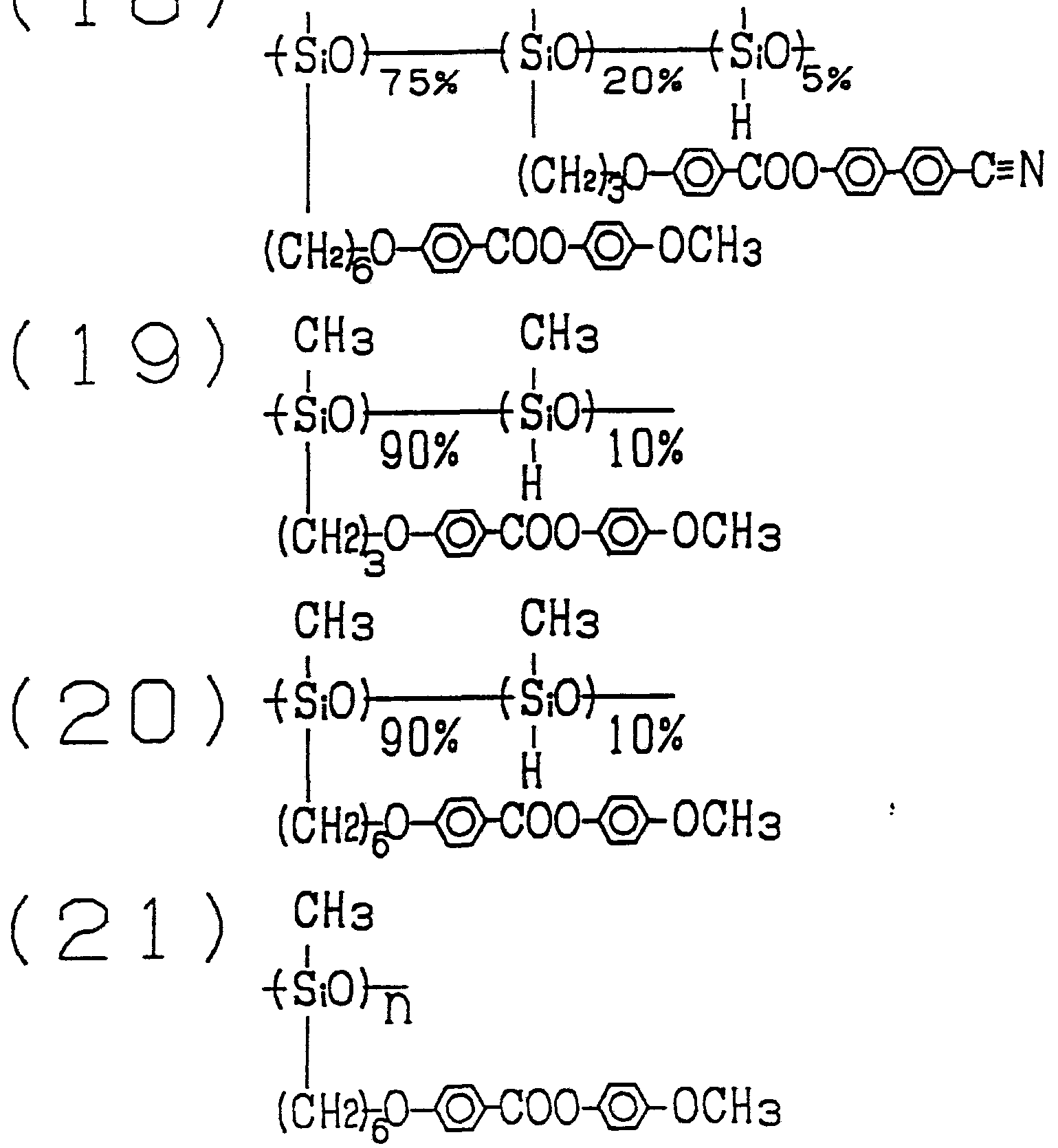
CH3
22

(CH2)#H§ :00- -F
CH3

CH3-C-C00 (CH2)60-O C00-g-0CH3
28 80%
、
CH3-C-C00 (CH2)6CHg C〇CH^C2H5 ίΗ220%
Z 06AV 081
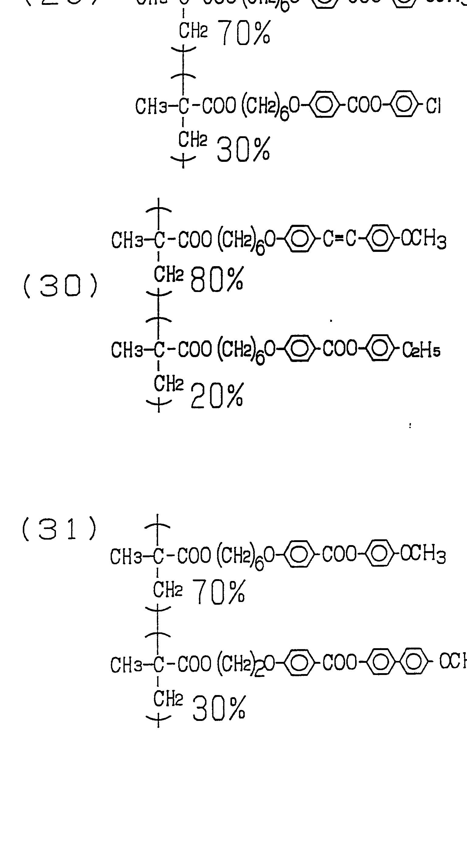
0 O
CM 00 00


siH90H02HOOO0<g-OO0©-eiH90 SHO (S)280I-S 8E
(S) 51-80 εΗ0 丄 ε) πΗ50<§)-000© 0Η0εΐΗ90
εΗΟ 9ε

(S) 02 -WO
08IW/Z6 OAV
- 02 -
CM21 (R)
43) CH3

cn
ΓΌ 00


55)

以上述べた 様 に、 本発明 の 液晶装置 は、 液晶高分子膜 を 光学異 方体 に 用 い る こ と を 特徴 と し て い る。 そ こ で、 本光学異方体 を 備え た 液晶装置の 着色補償 に つ いて 以下
に簡単 に説明す る。 本発明の液晶装置の O F F 状態 の光 学特性の説明図 を第 3 3 図 に 示 し た。 第 3 1 図 と 第 3 3 図 を比較す る と 第 3 3 図 は、 液晶高分子膜か ら な る 光 学 異 方体が構成要素 に含 ま れて い る 点が第 3 1 図 と 異 な つ て い る。 説明 を 簡単 に する た め、 光学異 方体 5 4 と 偏光 板 8 を 除 く 構成要素の 条件は第 3 1 図 に 示 さ れた従来の S T N液晶装置の例、 すな わち第 3 2 図 に そ の ス ぺ ク ト ルが示 さ れて い る S T N液晶装置 と 同一 で あ る と す る。 従っ て、 表示セ ル 5 5 を通過 し た後の各波長の 偏光状態 7 5、 7 6、 7 7 は、 第 3 3 図の場合 も 第 3 1 図の 6 5, 6 6、 6 7 と 全 く 同一 であ る。 異な っ て い る の は、 第 3 3 図の場合の各偏光 7 5、 7 6、 7 7 が次 に通過す る の が光学異方体 5 4 であ る と い う 点であ る。 本発明に お い て は、 こ の光学異方体 5 4 が、 偏光 7 5、 7 6、 7 7 が 表示セ ル 5 5 を 通過する事に よ っ て 生 じ た波長分散を キ ヤ ンセ ルする 作用を有 して い る の で あ る。 し た がっ て、 偏光 7 5、 7 6、 7 7 は光学異方体を 通過する 事に よ り、 各 々 7 8、 7 9、 8 0 の様な 直線僞光 に戻 り、 さ ら に偏 光板を通過す る 事に よ り、 各 々 8 1、 8 2、 8 3 の様な 直線偏光 と し て 出射す る。 そ して、 こ の 時の 出射光の ス ベ ク ト ル を第 7 図 に 示 し た。 こ の様 に 本発明の 液晶装置 で は 0 F F状態の着色現象を 解消す る 事が で き る。 ま た、 〇 N の 時 も 後述の実施例に よ る 多数の 実験結果 と コ ン ピ ュ 一 タ シ ユ ミ レ ー シ ョ ン に よ り、 レ、 ろ い ろ の 条 件 に 於 レ て 着色が無い事 を確認 し て い る。 こ の 時の 条件は、
( 1 ) 表示 セ ルの n d と 光学 異 方体の Δ η d の 値が ほ ぼ等 し い。
( 2 ) 表示セ ルの ッ イ ス ト 角 を 0 と す る と 光学異 方体 の捻れ角 は ほ ぼ一 0 で あ る,
( 3 ) 第 6 図 に お け る光学異方体の表示 セ ル と 対 向 す る 表面 の 光軸 方向 1 1 と 表示セ ル の 上側電極基板の ラ ビ ン グ方 向 1 0 の なす角度は約 9 0 度で あ る。
以上の 条件が少 な く と も 成 AL し た 場合 に は、 上記の よ う に 着色現象を解消す る事がで き る。 こ れ ら の光学特性の 改善に つ いて は、 特公平 3 8 1 4 6 に詳細 に開示 さ れた 2 層型ス 一パ一ッ イ ス 卜 ネ マ チ ッ ク 液晶セ ルの 光学 補僙効果 と 同様であ る の で詳細は省略す る が、 こ の 様 に し て得 ら れた 発 の液晶装置 に お いて は、 一対の 偏光 板の一力 通過 し て き た 直線傭光が表示セ ル と 色補償板 の少な く と ¾ 2 層を 通過 ""3 る た め、 S T N 表示セ ル の複 屈折性 と 旋光性 に よ る 着色が解消 さ れ約 4 0 0 n m か ら 7 0 0 n m の 範囲の波長域で は長軸方向 の ほ ぼ揃っ た楕 円僱光 と な る , し た がつ て う 一 方の偏光板 を通過 し た と き に は特定の波長域が遮断 さ れ る こ と は な く、 結果 的 に は偏光板 を 通過 し た後の 光は 白色に 近 い色 と な る。
すな わ ち、 本発明の光学異 方体 と 光学 ^方体の製造方 法 と、 光学異方体を 備 え た液晶装置 と 光学異方体を 備 え た液晶装置 の 製造方法 に お い て は、 従来の 2 層型ス ー パ ー ネ マ チ ッ ク 液晶装置 の コ ン ト ラ ス 卜 と 視野角等の 表示 特性 を 損 な う 事な く、 かつ、 小型薄型化 モ 実現す る 液曰曰
装置を 安価に提供す る事がで き る。 図面の簡単な説明
第 1 図 は本発明の 実施例 1 に於 け る 光学異方体の 一例 の 断面の略図、 第 2 図 は本発明の 実施例 2 に於 ける 光学 異方体の 一例の断面の略図、 第 3 図 は本発明の 実施例 3 に於け る 光学異方体の一例の 断面の略図、 第 4 図は 本発 明の実施例 4 に於ける 光学異 方体の一例の断面の略図、 第 5 図 は本発明の実施例 1 で得 ら れた光学異方体を 備え た液晶装置の一例の断面の 略図で あ る。 第 6 図 は液晶の 配 向方向及び、 傭光板の吸収軸の 方向、 液晶高分子の分 子長軸の 方向 を 示 し た 図であ る。 第 7 図 は本発明の 液晶 装置の コ ン ト ラ ス ト 曲線を 示 し た 図 であ る。 第 8 図 は本 発明の実施例 2 で得 ら れた光学異方体を備え た液晶装置 の一例の断面の略図、 第 9 図 は本発明の実施例 3 で得 ら れた光学異方体を備えた液晶装置の一例の 断面の略図、 第 1 0 図 は本発明の実施例 4 で得 ら れた光学異方体 を備 え た液晶装置の一例の断面の略図、 第 1 1 図は本発明の 実施例 9 の光学異方体を備え た液晶装置の 一例の断面の 略図で あ る。 第 1 2 図 は本発明の 実施例 1 0 の 光学異 方 体を備え た液晶装置の 一例の 断面の略図、 第 1 3 図 は本 発明の 実施例 1 1 の光学異方体を 備え た 液晶装置の 一例 の 断面の略図、 第 1 4 図 は本発明 の 実施例 1 2 の光学異 方体を 備え た液晶装置の一例の断面の略図 で あ る。 第 1 5 図は本発明の 実施例 1 の 光学異方体の 製造方法の 一例
を 示 し た 図、 第 1 6 図 は本発明の 実施例 2 の 光学異 方体 の 製造方法の 一例を 示 し た 図、 第 1 7 図 は本発明の 実施 例 3 の 光学異 方体の 製造方法の一例 を 示 し た 図 であ る。 第 1 8 図 は本発明 の 実施例 4 の光学異 方体の 製造方 法の 一例を 示 し 図、 第 1 9 図 は本発明 の 実施例 1 8 の 光学 異 方体の 製造方法の 一例を 示 し た 図、 第 2 0 図 は本発明 の 実施例 1 9 の 光学異 方体の 製造方法の 一例を 示 し た 図 第 2 1 図 は本発明の 実施例 2 5 の 光学異方体を 備え た液 晶装置 の 製造方法の 一例の略図で あ る。 第 2 2 図は 本発 明の 実施例 3 1 の光学異方体を 備 え た液晶装置 の製造方 法の一例の略図、 第 2 3 図 は本発明 の実施例 3 2 の 光学 異方体を 備え た液晶装置の製造方法の 一例 の略図、 第 2 4 図 は本発明の 実施例 3 3 の 光学異方体 を 備え た液晶装 置の製造方法の 一例の略図、 第 2 5 図 は 本発明の実施例 3 4 の 光学異方体を 備えた液晶装置の製造方法の一例の 略図で あ る。 第 2 6 図 は本発明の 実施例 3 5 の 光学異方 体を備 え た液晶装置の 製造方法の 一例の 略図、 第 2 7 図 は本発明の実施例 3 6 の光学異方体を備え た液晶装置の 製造方法の一例の略図、 第 2 8 図 は本発明 の 実施例 3 7 の 光学異方体 を 備 え た液晶装置の 製造方法 の 一例の 略図. 第 2 9 図 は本発明の 実施例 3 8 の 光学異 方体 を 備え た液 晶装置 の 製造 方法の 一例の 略図 で あ る。 第 3 0 図 は従来 の 白黒表示液晶装置 の 断面の 略図、 第 3 1 図 は従来 の S T N 液晶装置 の O F F 状態の 光学 的特性 の 説明図。 第 3 2 図 は従来の S T N 液晶装置 の ス ぺ ク ト ル を 表 し た 図 で
あ る。 第 3 3 図 は本発明の液晶装置の O F F 状態の 光学 的特性の 説明図。 第 3 4 図 は従来の 3 丁 液晶装置 の視 野角 と コ ン ト ラ ス ト を 示 し た 図、 第 3 5 図 は本発明 の液 晶装置の視野角 と コ ン ト ラ ス ト を 示 し た 図 であ る。 第 3 6 図 は本発明の 実施例 に お け る液晶表示 セ ル と 光学異方 体の望 ま し い範囲の 一例を 示 し た 図、 第 3 7 図 は本発明 の 実施例 にお け る液晶表示セ ル と 光学異方体の望ま し い 範囲の 一例を 示 し た 図、 第 3 8 図 は本発明の実施例 に お け る液晶表示セ ル と 光学異方体の望 ま し い範囲の一例を 示 し た図、 第 3タ 図 は本発明の実施例に お け る 液晶表示 セ ル と 光学異方体の望 ま し い範囲の一例 を 示 し た図、 第 4 0 図 は本発明の実施例に お け る 液晶表示セ ル と 光学異 方体の望 ま し い範囲の一例を 示 し た 図、 第 4 1 図は 本発 明の実施例に お ける液晶表示セ ル と 光学異方体の望 ま し い範囲の一例を 示 し た 図であ る。 発明を 実施す る た めの最良 の形態
以下添付図面を参照 して本発明の 実施例を説明す る
( 実施例 1 ) 本発明の 光学異方体の 一例の 断面 の略 図 を第 1 図 に示 し た。 透明 な 基板 1 上 に ポ リ イ ミ ド 薄膜 2 ( 東 レ 社製 S P 7 4 0 ) が形成 さ れて お り、 こ の基 板 1 上の ポ リ ィ ミ ド薄膜 2 は一軸方向 に ラ ビ ン グ処理が さ れて レヽ る。 こ の ポ リ イ ミ ド 薄膜 2 上 に は、 約 6 m の. 先 に示 し た シ ロ キ サ ン鎖を 骨格 に有す る ネ マ チ ッ ク 相 を
示す側鎖型液晶高分子 ( 3 ) と ( 2 ) の 9 5 % : 5 % 混 合物 に、 不整 中心 を 有す る 光学活性化合物 で あ る メ ル ク 社製 C B — 1 5 ( 3 7 ) を 5 % 添力 Π し た 液晶高分子膜 3 が形成 さ れて い る。 こ の液 晶高分子膜 3 は ね じ れ方 向右 回 り 2 3 0 度 に ツ イ ス ト 配 向 し て い る。 本発明 の光 学異 方体は、 S T N 液晶セ ル の、 そ の 液晶の 捻れ に よ る 旋光 性 と 複屈折性 を 原因 と す る 着色を 補償す る 効果があ り、 液晶装置 の高 コ ン ト ラ ス ト 化、 高視野化 を 実現す る 事が で き た。
( 実施例 2 ) 本発明の光 異 体の 一例の 断面 の 略 図 を 第 2 図 に 示 し た。 透明 な 基板 1 上 に は、 一軸方 向 に ラ ビ ン グ処理が さ れて い る。 こ の透明な 基板 1 上に、 約 6 m の. . 先 に示 し た シ ロ キ サ ン鎖を 骨格 に有する ネ マ チ ッ ク 相 を 示す側鎖型液晶髙分子 ( 3 ) と ( 2 ) の 9 5 % : 5 % 混合物 に、 不整中心 を有す る 光学活性化合物で あ る メ ル ク 社製 C B - 1 5 ( 3 7 ) を 5 % 添加 し た 混合 物 の液晶高分子膜 3 が形成 さ れて い る β こ の液晶高 分子 膜 3 は、 ね じ れ方向右 回 り 2 3 0 度 に ツ イ ス 卜 配向 し て い る。 本発明 の 光学異 方体 は. S T N 液晶 セ ル の、 モ の 液晶の 捻 れ に よ る旋光性 と 複屈折性 を 原 因 と す る 着色 を 補償す る 効果が あ り、 液晶装置の 高 コ ン ト ラ ス ト 化、 高 視野角化 を 実現す る 事がで き た。
( 実施例 3 ) 本発 明 の 光学異 方体の 一例の 断面 の 略
図 を第 3 図 に示 し た。 透明 な基板 1 上に ボ リ イ ミ ド 薄膜 2 ( 東 レ 社製 S P 7 4 0 ) が形成 さ れて お り、 こ の基 板 1 上の ボ リ ィ ミ ド薄膜 2 は一軸方向 に ラ ビ ン グ処理が さ れて い る。 こ の ポ リ イ ミ ド薄膜 2 上 に、 約 6 >u m の、 先 に示 し た シ ロ キ サ ン鎖を 骨格に有す る ネ マ チ ッ ク 相を 示す側鎖型液晶高分子 ( 3 ) と ( 2 ) の 9 5 % : 5 %混 合物に不整中心を有す る 光学活性化合物で あ る メ ル ク 社 製 C B — 1 5 ( 3 7 ) を 5 %添加 し た液晶高分子膜 3 が 形成さ れて い る。 さ ら に、 こ の液晶高分子膜 3 の上 に は 光学異方性の な い保護膜 4 が形成 さ れて い る。 本発明の 光学異方体は、 S T N液晶セ ルの、 そ の液晶の捻れ に よ る 旋光性 と 複屈折性を原因 と する 着色を補償す る効果が あ り、 液晶装置の高 コ ン ト ラ ス ト 化、 高視野化を実現す る事がで き た。
( 実施例 4 ) 本発明の光学異方体の一例の断面の略 図 を第 4 図 に示 した。 透明な基板 1 上に は、 一軸方向 に ラ ビ ング処理が さ れて い る。 こ の透明な基板 1 上に、 約 6 m の、 先 に示 し た シ ロ キ サ ン鎖を 骨格 に有する ネ マ チ ッ ク 相を示す側鎖型液晶高分子 ( 3 ) と ( 2 ) の 9 5 % : 5 % 混合物 に、 不整中心 を有す る 光学活性化合物で あ る メ ル ク社製 C B - 1 5 ( 3 7 ) を 5 %添加 し た 混合 物であ る 液晶高分子膜 3 が形成さ れて い る。 さ ら に こ の 液晶高分子膜 3 の上 に は、 透明な光学異方性の な い 保護 膜 4 が形成 さ れて い る。 一方 こ の液晶高分子膜 3 は、 ね
じ れ方向右回 り 2 3 0 度 に ツ イ ス ト 配 向 し て い る。 本発 明 の 光学異方体 は、 S T N 液晶セ ル の、 そ の液晶の 捻れ に よ る 旋光性 と 複屈折性を 原 因 と す る 着色 を補償す る 効 果が あ り、 液晶装置 の 高 コ ン ト ラ ス ト 化、 高視野角 化 を 実現す る 事がで き た。
( 実施例 5 ) 実施例 1 で得 ら れ た光学異方体を 備 え た 本発明の液晶装置の 一例の 断面の 略図 を 第 5 図 に 示 し た。 同 5 に於 い て、 透明電極 5 1 と 液晶配 向膜 5 2 を 有 す る液晶セ ル の透明基板 5 は ス べ ー サ ー 6 を 介 し て 張 り 合わせて あ り、 その間 に液晶 ( メ ル ク 社製 Ζ L I 4 5 0 6 ) 7 が真空注入 さ れて い る。 本光学異方体 と 液晶セ ル は、 2 枚の偏光板 8 の間 に設置 さ れて い る。 その 時の 液晶の配向方向及び、 偏光板の吸収軸の 方向、 液晶髙分 子の分子長軸の 方向 を 第 6 図 に示 し た。 第 6 図 に於 て、 9 は第 5 図 に お ける 液晶表示セ ル の 下側 % 板の ラ ビ ン グ方向 1 0 は第 5 図 に お け る 液晶表示セ ル の上側電 極基板の ラ ビ ン グ方向 . 1 1 は第 5 図 に お け る 液晶高分 子膜 3 の液晶表示セ ル に隣接す る 液晶分子の長軸方 向、 1 2 は第 5 図 に お け る 液晶高分子膜 3 の 上側偏光板 8 に 隣接す る 液晶分子の 長軸方 向、 1 3 は第 5 図 に お け る 下 側偏光板 8 の偏光軸 ( 吸収軸 ) の 方 向、 1 4 は . 第 5 図 に お け る 上側偏光板 8 の偏光軸 ( 吸収軸 ) の 方 向、 1 5 は第 5 図 に お け る 液 Β - Θ-曰表示 セ ル の ね じ れ角 の 大 ぎ さ、 1 6 は方向 1 1 と 方向 0 の な す角度、 1 7 は 1 4 と 方向
1 2 の な す角度、 1 8 は方向 9 と 方向 1 3 の な す角 度、 1 9 は方向 1 2 と 方向 1 1 の なす角度で あ る。 本実施例 では上記条件を 以下の様に設定 し て い る。 角度 1 6 を 9 0 度、 角度 1 7 は 4 5 度であ る。 ま た、 第 5 図 にお け る 液晶表示セ ル の ね じ れ角 1 5 を約 2 0 0 度の左ね じ れ、 第 5 図 にお け る液晶表示セ ル 内の液晶の Δ η X d が 0. 8 5 m と であ る。 そ の後液晶駆動用 ド ラ イ バー及び液 晶駆動用回路を上記液晶セ ル に接続 して、 照明用光源を 液晶セ ル の背後に設置 し液晶装置 を 組み立て た。 本液晶 装置 に、 O N, O F F電圧 に相当 す る 電圧を 印加 し た と こ ろ、 白黒表示が確認でき た。 そ の時の コ ン ト ラ ス ト 曲 線を第 7 図 に示 し た。 一方 コ ン ト ラ ス ト と 視野角の 関係 を第 3 4 図に示 した, 同図において、 ( D ) 、 ( E )、 ( F ) はそれぞれ、 従来の 2 層型ス ーパーツ イ ス ト ネ マ チ ッ ク 液晶装置、 一軸延伸フ ィ ル ム を一枚用い た液晶装 置、 一軸延伸フ ィ ルム を 2 枚用 い た液晶装置の コ ン ト ラ ス ト と 視野角 の 闋係を表 し て い る。 本実施例 に お い て作 成 した光学異方体を備えた液晶装置の、 コ ン ト ラ ス ト と 視野角 の 関係を第 3 5 図 に示 し た。 明 ら か に液晶装置の 視野角特性が向上 し た液晶装置が得 ら れた。
( 実施例 6 ) 第 8 図 に実施例 2 の光学異方体を 用 い た液晶装置の 一例の断面の略図を 示 し た。 同図 に於 いて、 透明電極 5 1 と 液晶配 向膜 5 2 を 有す る 液晶セ ルの 透明 基板 5 は ス ぺー サー 6 を介 し て張 り 合わせて あ り、 そ の
間 に液晶 ( メ ル ク 社製 Z L 1 4 5 0 6 ) 7 が真空注入 さ れて い る。 本光学異方体 と 液晶表示セ ル は、 2枚 の偏 光板 8 の 間 に設置 さ れて い る。 次 に 示 し た 以外の構成 は 実施例 5 と 同様であ る の で、 本実施例で は 上記条件 を 以 下 の様 に設定 し て い る。 角度 1 6 を 8 5 度、 角度 1 7 は 4 5 度で あ る。 ま た、 液晶表示セ ル の ね じ れ角 1 5 を 約 2 0 0 度の左ね じ れ、 液晶表示セ ル 内の液晶 7 の Δ η χ d が 0. 8 5 yu mで あ る。 そ の後液晶駆動用 ド ラ イ バー 及び液晶艇動用 回路 を 上記液晶セ ル に接続 し て、 照 明用 光源を 液晶セ ル の背後 に設置 し液晶装置 を 組み立て た。 本液晶装置に、 O N, O F F 電圧 に相当 す る 電圧を 印加 し た と こ ろ、 白黒表示が確認で き 実施例 5 と 同様の 表示 特性が得 ら れた。
( 実施例 7 ) 第 9 図 に 実施例 3 の光学異方体を 用 い た液晶装置の 一例の断面の 略図 を 示 し た。 図 9 に於 い て、 透明電極 5 1 と 液晶配向膜 5 2 を 有す る 液晶セ ルの 透明 基板 5 は ス ぺーサー 6 を介 し て張 り 合わせて あ り、 そ の 間 に液晶 ( メ ル ク 社製 Z L I 4 5 0 6 ) 7 が真空注入 さ れて い る。 本光学異 方体 と 液晶表示セ ル は、 2 枚 の偏 光板 8 の 間 に 設置 さ れて い る。 そ の 時の液晶の配向 方向 及び、 偏光板の 吸収軸 の方 向、 液晶高分子の分子長 軸の 方 向 は 実施例 5 と 同様 に し た。 角度 1 6 を 8 0 度、 角度 1 7 は 5 0 度で あ る。 ま た、 液晶表示セ ル の ね じ れ 角 1 5 を 約 2 3 0 度の左ね じ れ、 液晶表示セ ル 内の 液晶 7 の
△ n x d が 0. 8 5 y m で あ る。 そ の後液晶駆動用 ド ラ イ ノて一及び液晶駆動用 回路 を 上記液晶セ ル に接続 し て、 照明用光源を 液晶セ ル の背後 に設置 し液晶装置 を組 み立 て た。 本液晶装置 に、 0 N, O F F 電圧 に相当 する 電圧 を 印加 し た と こ ろ、 白黒表示が確認で き 実施例 5 と 同様 の表示特性が得 ら れた
( 実施例 8 ) 第 1 0 図 に 実施例 4 の 光学異方体 を用 い た液晶装置の一例の断面の 略図 を 示 し た。 第 1 0 図 に 於いて、 透明電極 5 1 と 液晶配向膜 5 2 を有す る液 晶セ ルの透明基板 5 はス ベーサ ー 6 を 介 して張 り 合わせ て あ り、 そ の 間に液晶 ( メ ル ク 社製 Z L I 4 5 0 6 ) 7 が 真空注入さ れて い る。 本光学異方体 と 液晶表示セ ル は、 2 枚の偏光板 8 の間 に設置 さ れて い る。 そ の時の液晶の 配向方向及び、 偏光板の吸収軸の 方向、 液晶高分子の分 子長軸の 方向 は実施例 5 と 同様に し た。 本実施例で は上 記条件を 以下の様に設定 し て い る。 角度 1 6 を 9 0 度、 角度 1 7 は 4 5 であ る。 ま た、 液晶表示セ ルの ね じ れ角 1 5 を約 2 4 0 度の左ね じ れ、 液晶表示セ ル内の液晶 7 の 厶 n X d が 0. 8 5 m で あ る。 そ の後液晶駆動用 ド ラ イ バー及び液晶駆動用 回路を上記液晶セ ル に接続 し て、 照明用光源を液晶セ ル の背後 に設置 し液晶装置 を組 み立 て た。 本液晶装置 に、 0 N, 0 F F 電圧 に相当 する 電圧 を 印加 し た と こ ろ、 白黒表示が確認で き 実施例 5 と 同様 の 表示特性が得 ら れた。
( 実施例 9 ) 本発明の液晶装置 の 一例 の 断面の 略図 を 第 1 1 図 に 示す。 同 図 に お いて、 透明電極 5 1 と 液晶 配 向膜 5 2 を 有す る 液晶セ ル の透明基板 5 は ス ぺー サ ー
6 を介 し て張 り 合わせて あ り- そ の 間 に 液 ΒΒ ( メ ル ク 社 製 Z L I 4 5 0 6 ) 7 が真空注入 さ れて い る。 こ の、 液晶表示セ ル の液晶 に 接 し な い液晶 セ ル の透明基板 5 上 に は、 ボ リ ィ ミ ド薄膜 2 ( 東 レ社製 S Ρ 7 4 0 ) が形 成 さ れて お り, こ の透明基板 5 上の ポ リ イ ミ ド 薄膜 2 は —軸方 向 に ラ ビ ン グ処理が さ れて い る。 こ の ポ リ ィ ミ ト' 薄膜 2 上 に、 約 6 / m の、 先 に示 し た シ 口 キ サ ン鎖 を 骨 格 に有す る ネ マ チ ッ ク 相を 示す側鎖型液晶高分子 ( 3 ) と ( 2 ) の 9 0 % : 1 0 % 混合物 に、 不整 中 /[ を有す る 光学活性化合物であ る メ ル ク 社製 C Β - 1 5 ( 3 7 ) を 5 %添加 し た液晶高分子膜 3 が形成 さ れて い る。 こ の液 晶 fe分子膜 3 はね じ れ方向右 回 り 2 3 0 度 に ッ ィ ス ト 配 向 し て い る。 光学異方体を 備え た液晶表示セ ルは、 2 枚の傭光板 8 の 間 に設置 さ れて い る。 モ の時の液晶 の配 向 方向及び、 偏光板 の 吸収軸 の 方向、 液晶高分子の 分子 長軸の 方 向 は 実施例 5 と 同様 に し た 本実施例では 上記 条件を 以下の係 に sx し て い る。 角度 1 5 を 8 9 度、 角 度 1 7 は 4 5 度であ る , ま た 液晶表示 セ ル の ね じ れ角 1 5 を 約 2 0 0 度の 左 ね じ れ. 液 白
曰 θ曰表示 セ ル 内 の液 晶 7 の Δ n X d が 0 . 8 5 y m で る。 そ の後液晶駆動用 ド ラ ィ バ一及び液晶駆動用 回路 を 上記液晶 セ ル に 接航 し て
照明用光源を液晶セ ル の背後 に設置 し液晶装置 を組 み立 て た。 本液晶装置 に、 O N, O F F 電圧 に相当 す る 電圧 を 印加 し た と こ ろ、 白 黒表示が確認で き 実施例 5 と 同様 の 表示特性が得 ら れた。
( 実施例 1 0 ) 本発明の液晶装置の一例の 断面の略 図 を第 1 2 図 に示す。 同図 に お い て、 透明電極 5 1 と 液 晶配向膜 5 2 を有する 液晶表示セ ル の透明基板 5 は ス べ ー サー 6 を介 し て張 り 合わせて あ り、 そ の 間に液晶 ( メ ル ク 社製 Z L I 4 5 0 6 ) 7 が真空注入 さ れて い る。 こ の液晶表示セ ルの液晶に接 し な い透明基板 5 上に は、 一軸方向 に ラ ビ ン グ処理が さ れて い る。 透明基板 5 上 に、 約 6 mの、 先 に示 し た シ ロ キ サ ン鎖を 骨格 に有す る ネ マ チ ッ ク 相を示す側鎖型液晶高分子 ( 3 ) と ( 2 ) の 9 0 % ·· 1 0 %混合物 に、 不整中心 を有す る 光学活性化合 物であ る メ ル ク 社製 C B — 1 5 ( 3 7 ) を 5 %添加 し た 液晶高分子膜 3 が形成 さ れて い る。 こ の液晶高分子膜 3 はね じ れ方向右回 り 2 3 0度に ツ イ ス ト 配向 して い る。 本光学異方体を 備え た液晶表示セ ル は、 2 枚の偏光板 8 の 間 に設置 さ れて い る。 そ の 時の液晶 の配 向方向及び、 偏光板の 吸収軸の 方向、 液晶高分子の分子長軸の方 向 は、 実施例 5 と 同様 に し た。 本実施例で は上記条件を以下の 様 に設定 して い る。 角度 1 6 は 8 5 度、 角度 1 7 は 4 5 度であ る。 ま た、 液晶表示セ ル の ね じ れ角 1 5 を約 2 3 0 度の 左ね じ れ、 液晶表示セ ル 内の 液晶 7 の Δ n X d 力 ί
0. 8 5 m で あ る。 そ の 後液晶駆動用 ド ラ イ バー 及び 液晶駆動用 回路 を 上記液晶 セ ル に 接続 し て、 照 明用 光源 を 液晶 セ ル の 背後 に 設置 し 液晶装置 を 組み 立て た。 本液 晶装置 に、 O N, 0 F F 電圧 に相 当 す る 電圧 を 印加 し た と こ ろ、 白黒表示が確認で き 実施例 5 と 同様の 表示特性 が得 ら れ た。
( 実施例 1 1 ) 本発明の 液晶装 置の 一例の 断面 の 略 図 を第 1 3 図 に 示す。 同図 に お い て、 透 明電極 5 1 と 液 晶配向膜 5 2 を 有す る 液晶セ ル の 透 明基板 5 は ス ぺ ー サ — 6 を 介 し て 張 り 合 わせて あ り、 そ の 間 に 液晶 ( メ ル ク 社製 Z L I 4 5 0 6 ) 7 が真空注入 さ れて い る。 こ の、 液晶表示セ ル の 液晶 7 に接 し な い液晶表示 セ ル の透 明基 板 5 上 に は、 ポ リ イ ミ ド薄膜 2 ( 東 レ 社製 S P 7 4 0 ) が形成 さ れて お り、 こ の透明基板 5 上の ポ リ ィ ミ ド 薄膜 2 は一軸方向 に ラ ビ ン グ処理が さ れて い る。 こ の ポ リ ィ ミ ド薄膜 2 上 に、 約 6 m の、 先 に 示 し た シ ロ キ サ ン鎖 を 骨格 に 有す る ネ マ チ ッ ク 相 を 示 す 側鎖型液晶 高分子
( 3 ) と ( 2 ) の 9 0 % : 1 0 % 混合物 に、 不整中 心 を 有す る 光学活性化合物 で あ る メ ル ク 社製 C B — 1 5 ( 3 7 ) を 5 % 添加 し た 液晶高分子膜 3 が形成 さ れ て い る。 さ ら に、 こ の 液晶高分子膜 3 の 上 に は光学異 方性を 持 た な い保護膜 4 が形成 さ れて い る。 一 方 こ の 液晶高分子膜 3 は ね じ れ方 向右 回 り 2 3 0 度 に ツ イ ス ト 配 向 し て レ、 る。 本光学異 方体 を 備え た 液晶表示セ ル は、 2 枚の 偏光板 S
の 間 に設置さ れて い る。 そ の 時の液晶の配 向方向及び、 偏光板の 吸収軸の 方向、 液晶高分子の分子長軸の方 向 は 実施例 o に従っ た , 本実施例では上 S己条件を 以下の 様 に 設定 し て い る。 角度 1 6 は 1 0 0 度、 角度 1 7 は 4 5 度 で あ る , ま た、 液 B BH表示セ ル の ね じ れ角 1 5 を約 2 0 0 度の左ね じ れ、 液日日 セ ル 内の液晶 7 の Δ η X d が 0 , 8 5 m であ る。 そ の後液晶駆動用 ド ラ ィ バ一及び液晶 駆動用回路を 上記液晶セ ル に接続 し て、 照明用光源 を 液 晶セ ルの 背後 に設置 し液晶装置を組み立て た。 本液晶装 置 に、 O N , O F F 電圧に相 当す る 電圧を 印加 した と こ ろ、 白黒表示が確認で き実施例 5 と 同様の 表示特性が得 ら れた <
( 実施例 1 2 ) 本発明の液晶装置の一例の断面の略 図 を第 1 4 図 に示す。 同図 にお いて、 透明電極 5 1 と 液 晶配向膜 5 2 を有す る液晶セ ルの透明基板 5 は ス ベ ーサ 一 6 を介 して張 り 合わせて あ り、 そ の間 に液晶 ( メ ル ク 社製 Z L I 4 5 0 6 ) 7 が真空注入 さ れて い る。 こ の、 液晶表示セ ルの液晶 7 に接 し な い液晶表示セ ルの透 明基 板 5 上 に は、 一軸方向 に ラ ビ ン グ処理が さ れて い る。 さ ら に、 こ の液晶表示セ ルの透明基板 5 上 に は約 6 m の, 先 に示 し た シ ロ キ サ ン鎖を 骨格 に有す る ネ マ チ ッ ク 相を 示す側鎖型液晶高分子 ( 3 ) と ( 2 ) の 9 0 % : 1 0 % 混合物 に、 不整 中心 を 光学活性化合物で あ "O メ ル ク 社製 C B - 1 5 ( 3 7 ) を 5 %添加 し た液晶高分子膜
3 が形成 さ れて い る。 さ ら に、 こ の 液晶高分子膜 3 の 上 に は光学異方性の な い保護膜 4 が形成 さ れて い る。 一 方 こ の液晶高分子膜 3 は ね じ れ方向右 回 り 2 3 0 度に ツ イ ス ト 配 向 し て い る。 本光学異 方体 を 備え た 液晶表示 セ ル は、 2 枚の偏光板 8 の 間 に設置 さ れて い る。 そ の時 の液 晶の配 向 方向及び、 偏光板の 吸収軸 の 方 向、 液晶高分子 の分子長軸の 方向 も 実施例 5 と 同様 と し た。 本実施例で は上記条件を 以下の様 に設定 し て い る。 角度 1 6 は 9 0 度、 角度 1 7 は 4 5 度であ る。 ま た、 液晶表示セ ル の ね じ れ角 1 5 を 約 2 0 0 度の 左 ね じ れ、 液晶表示 セ ル 内 の 液晶 7 の 厶 n x d が 0. 8 5 > m で あ る。 そ の後液晶駆 動用 ド ラ イ バー 及び液晶駆動用 回路 を 上記液晶セ ル に接 続 して、 照明用光源を 液晶セ ルの背後 に 設置 し液晶装置 を 組み立て た。 本液晶装置 に、 O N, O F F電圧に 相当 す る 電圧を 印加 し た と こ ろ、 白黒表示が確認で き 実施例 5 と 同様の表示特性が得 ら れた。
( 実施例 1 3 ) 実施例 5 か ら 1 2 に お いて、 偏光板 8 が液晶高分子膜 3 の 表面 あ る い は、 液晶高分子膜 3 上 の保護膜 4 と 有機材料か ら な る 粘着剤 を 介 し て 光学密着 し て い る 液晶装置 に お いて も、 同様の 光学特性が得 ら れ た。
( 実施例 1 4 ) 本発明 の 実施例 1 の 光学異 方体 の製 造方法の一例 を 第 1 5 図 に 示 し た。 透明基板 1 上に ポ リ
ィ 5 F ( 東 レ社製 S P 7 4 0 ) を 塗布 し、 基板を 加熱 し て硬化 さ せ、 ボ リ ィ ミ ド薄膜 2 を 形成 し た。 こ の 基板 上の ポ リ イ S 卜-薄膜 2 を ナ イ ロ ン ブ ラ シ 2 0 を 用い て一 方向 に 回転ラ ビ ングを 行い、 先に示 し た シ ロ キ サ ン鎖を 骨格に有する ネ マ チ ヅ ク相を 示す側鎖型液晶高分子 ( 3 ) と ( 2 ) の 9 0 % : 1 0 % 混合物 に.. 不整 中心 を有す る 光学活性化合物であ る メ ル ク 社製 C B - 1 5 ( 3 7 ) を 5 %添加 し た液 BB 同分子溶液 ( 固形分浪度 1 8 % ) を、 バー コ一タ ー 2 1 を用 いて塗布 し加熱 し て 溶媒を蒸発さ せ、 約 6 m の液晶高分子膜 3 を 得た。 そ の後、 8 0 °C で 3 時間加然配向 を 行い、 急冷 し て ね じ れ方向右回 0 2 3 0 度に ッ イ ス ト 配向 した光学異方体を得た。 液晶高分 子は広い範囲 に わた つ て均一 な配 向 を し て いた。 本光学 異方体を、 左 ま わ り 2 4 0 度ヅ イ ス ト 液晶セ ル の上 に各 軸方向を 実施例 5 と 同様に し て設置 し て重ね、 液晶 セ ル に電圧を 印加 し た と こ ろ、 白黒に近い表示が得 ら れ. S T N液晶表示体の 白黒表示が可能で め る と が確認で き た。
( 実施例 1 5 ) 本発明の 実施例 2 の 光学異方体 の 製 造方法の 一例を第 1 6 図 に示 し た。 透明基板 1 上を ナ イ ロ ン ブ ラ シ 2 0 を用 いて一方向 に 回転ラ ビ ン グを行 い、 先 に示 し た シ ロ キ サ ン鎖を骨格に有す る ネ マ チ ッ ク 相 を 示す側鎖型液晶高分子 ( 3 ) と ( 2 ) の 9 0 % : 1 0 % 混合物 に、 不整中心 を有す る 光学活性化合物で あ る メ ル
ク 社製 C B — 1 5 ( 3 7 ) を 5 % 添加 し た 液晶高分子溶 液 ( 固形分 ¾度 1 8 % ) を、 バー コ 一 タ ー 2 1 を用 い て 塗布 し加熱 し て 溶媒 を 蒸発 さ せ、 約 /" m の 液晶高分子膜 3 を得 た。 そ の後、 8 0 eCで 3 時間加熱配 向 を 行い、 急 ^ し て ね じ れ方向右 回 り 2 3 0 度 に ツ イ ス ト 配 向 し た 光 学異方体を得 た。 液晶高分子 は広 い範囲 に わ た っ て 均一 な 配向 を し て い た。 本光学異方体を、 左 ま わ り 2 4 0 度 ッ イ ス ト 液晶セ ルの上 に各軸 方向 を 実施例 5 と 同様 に し て 設置 し て重ね、 液晶セ ル に 電圧 を 印加 し た と こ ろ、 白 黒 に近い表示が得 ら れ、 S T N 液晶表示体の 白 黒表示が 可能であ る こ と が確認で き た。
( 実施例 1 6 ) 本発明の 実施例 3 の 光学異方体 の製 造方法の—例を第 1 7 図 に示 し た。 透明基板 1 上に ポ リ イ ミ K ( 東 レ 社製 S P 7 4 0 ) を 塗布 し、 基板を 加熱 し て硬化 さ せ、 ポ リ ィ ミ ド薄膜 2 を 形成 し た。 こ の 基板 上の ボ リ イ ミ ド薄膜 2 を ナ イ ロ ン ブ ラ シ 2 0 を 用 い て 一 方向 に 回転ラ ビ ン グを 行い、 先 に示 し た シ ロ キ サ ン鎖を 骨格 に有す る ネ マ チ ッ ク 相 を 示す側鎖型液晶高分子 ( 3 ) と ( 2 ) の 9 0 % : 1 0 % 混合物 に、 不整 中心 を 有 す る 光学活性化合物で あ る メ ル ク 社製 C B — 1 5 ( 3 7 ) を 5 %添加 し た 液晶高分子溶液 ( 固形分浪度 1 8 % ) を、 バー コ 一 夕 一 2 1 を 用 いて 塗布 し加熱 し て 溶媒 を蒸 発 さ せ、 約 6 m の液晶高分子膜 3 を 得 た。 そ の後 . 8 0 °C で 3 時間加熱配 向 を 行 い、 急 ^ し て ね じ れ方向右 回 り 2
3 0 度 に ツ イ ス ト 配 向 し た光学異方体を 得 た。 さ ら に、 水溶性ア ク リ ル樹脂を 塗布 し保護膜 4 を形成 し た。 液晶 高分子は広 い範囲 に わ た っ て 均一 な配向 を し て いた。 本 光学異方体を、 左 ま わ り 2 4 0 度 ツ イ ス ト 液晶セ ル の上 に各軸方向を 実施例 5 と 同様 に し て設置 し て重ね、 液晶 セ ル に電圧を 印加 し た と こ ろ、 白 黒 に近 い表示が得 ら れ, S T N液晶表示体の 白黒表示が可能 であ る こ と が確認で き た。
( 実施例 1 7 ) 本発明の実施例 4 の 光学異方体の製 造方法の一例を第 1 8 図 に示 し た。 透明基板 1 上に ナ イ ロ ンブラ シ 2 0 を用 い て一方向 に 回転ラ ビ ン グを行 い、 先 に示 し た シ ロ キ サ ン鎖を 骨格に有する ネ マ チ ッ ク 相を 示す側鎖型液 ΘΘ ¾分子 ( 3 ) と ( 2 ) の 9 0 % : 1 0 % 混合物 に、 不整中心を有す る 光学活性化合物であ る メ ル ク 社製 C B - 1 5 ( 3 7 ) を 5 % 添加 し た液晶高分子溶 液 ( 固形分潢度 1 8 % ) を、 バー コ 一 夕 - 2 1 を用 いて 塗布 し加熱 し て溶媒を 蒸発さ せ、 約 6 > m の液 fe同分子 膜 3 を得た。 そ の後, 8 0 。Cで 3 時間加熱配向 を行 い、 急冷 し て ね じ れ方向右回 り 2 3 0 度 に ッ イ ス 卜 配向 し た 光学異方体を 得た。 さ ら に、 水溶性 ァ ク リ ル樹脂を 塗存 し保護膜 4 を形成 し た。 液晶高分子は広 い範囲 に わ た つ て均一 な配向 を し て い た。 本光学異 方体 を、 左 ま わ り 2 4 0 度ッ イ ス ト 液晶 セ ルの 上 に各軸方向 を 実施例 5 と 同 様 に し て設置 し て重ね、 液晶セ ル に 電圧 を 印加 し た と こ
ろ、 白 黒 に近 い表示が得 ら れ、 S T N液晶表示体の 白 黒 表示が 可能で あ る こ と が確認で き た。
( 実施例 1 8 ) 本発明 の 光学異 方体の 製造方法 の 一 例 を 第 1 9 図 に示 し た。 本実施例 の 透明基板 は、 延伸処 理 さ れ た プラ ス チ ッ ク 基板 を 用 い た。 透 明基板 1 上 に、 先 に示 し た シ ロ キ サ ン鎖を 骨格 に 有す る ネ マ チ ッ ク 相 を 示す側鎖型液晶高分子 ( 3 ) と ( 2 ) の 9 0 % : 1 0 % 混合物 に、 不整 中心 を 有す る 光学活性化合物であ る メ ル ク 社製 C B — 1 5 ( 3 7 ) を 5 %添加 し た液晶高分子溶 液 ( 固形分 ¾度 1 8 % ) を、 ノ ー コ ー タ ー 2 1 を用 い て 塗布 し加熱 し て溶媒を 蒸発 さ せ、 約 6 m の液晶高分子 膜 3 を 得た。 そ の後、 8 0 eCで 3 時間加熱配向 を行 い、 急泠 し て ね じ れ方向右 回 り 2 3 0 度 に ツ イ ス ト 配向 し た 光学異 方体を 得た。 液晶高分子は広 い範囲 に わ た っ て均 一 な配 向 を し て いた。 本光学異方体 を、 左 ま わ り 2 4 0 度 ツ イ ス ト 液晶セ ルの上に各軸方向 を 実施例 5 と 同 様 に し て設置 し て重ね、 液晶セ ル に電圧 を 印加 し た と こ ろ、 白黒 に近 い表示が得 ら れ、 S T N液晶表示体の 白黒表示 が可能 で あ る こ と が確認で き た。
( 実施例 1 9 ) 本発明 の 光学異 方体の 製造方法 の 一 例 を 第 2 0 図 に 示 し た。 本実施例 の 透明基板 は、 延伸処 理 さ れ た プラ ス チ ッ ク 基板 を 用 い た。 透 明基板 1 上 に、 先 に 示 し た シ ロ キ サ ン鎖を 骨格 に 有す る ネ マ チ ッ ク 相 を
示す側鎖型液晶高分子 ( 3 ) と ( 2 )' の 9 0 % : 1 0 % 混合物 に、 不整中心 を有す る 光学活性化合物で あ る メ ル ク 社製 C B — 1 5 ( 3 7 ) を 5 % 添加 し た 液晶高分子溶 液 ( 固形分瀵度 1 8 % ) を、 バー コ 一 夕 一 2 1 を用 い て 塗布 し加熱 し て 溶媒を 蒸発 さ せ、 約 6 m の液晶高分子 膜 3 を 得た。 そ の後、 8 0 °Cで 3 時間加熱配向 を行 い、 急泠 し て ね じ れ方向右 回 り 2 3 0 度 に ツ イ ス ト 配向 し た 光学異方体を得た。 さ ら に、 水溶性ア ク リ ル樹脂を 塗布 し保護膜 4 を形成 し た。 液晶高分子は広 い範囲 に わ た つ て 均一 な配向 を して い た。 本光学異方体を、 左 ま わ り 2 4 0 度ッ イ ス ト 液晶セ ル の 上 に各軸方向 を 実施例 5 と 同 様に し て設置 し て重ね、 液晶セ ル に電圧 を 印加 し た と こ ろ、 白黒 に近い表示が得 ら れ、 S T N液晶表示体の 白黒 表示が可能であ る こ と が確認でき た。
( 実施例 2 0 ) 実施例 1 8、 1 9 に お いて、 延伸 し た プラ ス チ ッ ク 基板 に、 光学異方性の負の材料 と 光学異 方性の性の材料の混合物を延伸 し た も の を用 い て も 同様 の効果が得 ら れた。
( 実施例 2 1 ) 実施例 1 8、 1 9 に お いて、 延伸 し た プラ ス チ ッ ク 基板 に、 光学異方性の 負 の材料 と 光学異 方性の正 の材料 を重ね た フ ィ ルム を 用 い て も 同様の 効果 が得 ら れた。
( 実施例 2 2 ) 実施例 1 8、 1 9 に お い て、 延伸 し た ブラ ス チ ッ ク 基板 に、 光学異 方性 を 持つ延伸 フ イ ル ム を そ の延伸軸が 直交す る よ う に重ね た フ ィ ル ム を用 い て も 同様の 効果が得 ら れ た。
( 実施例 2 3 ) 実施例 1 4、 1 5、 1 6、 1 7 に お い て、 透明基板 に無機ガ ラ ス を 用 い て も 同様の 効果 が得 ら れた。
( 実施例 2 4 ) 実施例 1 4、 1 5、 1 6、 1 7、 に お いて、 透明基板 に キ ャ ス ト 方で得 ら れた ブ ラ ス チ ッ ク 基板を 用 いて も 同様の効果が得 ら れた。
( 実施例 2 5 ) 本発明の 光学異方体を 備え た液晶装 置の製造方法の一例の概略を 第 2 1 図 に 示 し た。 液晶表 示セ ル の透明基板 5 上 に I T O か ら な る 透 明電極 5 1 を 1 0 0 0 A形成 し、 フ ォ ト 工程 に よ っ て 所望の パ タ ー 二 ン グを 行っ た の ち、 液晶配向膜 5 2 を形成 し透明電極 5 1 と 液晶配 向膜 5 2 を 有す る 液晶表示セ ル の透明基板 5 を 用意 し た。 ス ぺー サ ー 6 及び液晶 ( メ ル ク 社製 Z L エ ー 4 5 0 6 ) 7 を 介 し て 対 向す る 液晶表示セ ル の 透明 基板 5 上 も 同様 に透 明電極 5 1 を 形成 し た 後、 パ タ ー 二 ン グ し液晶配 向膜 5 2 を 形成 し、 電極が互 い に ほぼ 直角 と な る よ う に 組み立て た。 実施例 1 4 で製造 し た光 学異 方体を、 液晶表示セ ル 上 に設置 し、 2 枚の 偏光板 8 の 間
に挾持 し て、 液晶装置 を作製 し た。 そ の 時の液晶の 配 向 方向及び、 偏光板の 吸収軸の 方向、 液晶高分子の分子長 軸の方向 は、 実施例 5 と 同様に し た。 液晶 セ ル に電圧を 印加 し た と こ ろ、 白黒 に近 い表示が得 ら れ、 S T N 液晶 表示体の 白黒表示が可能であ る こ と が確認で き た。
( 実施例 2 6 ) 実施例 1 5 で製造 し た 光学異方体を、 実施例 2 5 と 同様に液晶表示セ ル と 組み合わせ る事 に よ つ て も 実施例 2 5 と 同様な表示特性が得 ら れた。
( 実施例 2 7 ) 実施例 1 6 で製造 し た光学異方体を、 実施例 2 5 と 同様に液晶表示セ ル と 組み合わせる事 に よ つ て も 実施例 2 5 と 同様な表示特性が得 ら れた。
( 実施例 2 8 ) 実施例 1 7 で製造 し た光学異方体を、 実施例 2 5 と 同様に液晶表示セ ル と 組み合わせ る事 に よ つ て も 実施例 2 5 と 同様な表示特性が得 ら れた。
( 実施例 2 9 ) 実施例 1 8 で製造 し た光学異方体を、 実施例 2 5 と 同様に液晶表示セ ル と 組み合わせ る事 に よ つ て も 実施例 2 5 と 同様な 表示特性が得 ら れた。
( 実施例 3 0 ) 実施例 1 9 で製造 し た 光学異方体を、 実施例 2 5 と 同様 に液晶表示セ ル と 組み合わせ る事 に よ つ て も 実施例 2 5 と 同様な 表示特性が得 ら れた。
( 実施例 3 1 ) 本発明 の 光学異 方体 を 備え た液 晶装 置 の製造方法の 一例の 略図 を 第 2 2 図 に 示 し た。 液 晶表 示セ ル の 透明基板 5 上 に I T 〇 か ら な る 透 明電極 5 1 を 1 0 0 0 A形成 し、 フ ォ ト 工程 に よ っ て 所望の パ タ ー 二 ン グを 行 っ た の ち、 液晶配 向膜 5 2 を形成 し透明電極 5 1 と 液晶配向膜 5 2 を 有す る 液晶表示セ ル の透明基板 5 を 用意 し た。 ス ベー サ ー 6 及び液晶 ( メ ル ク 社製 Z L 1 - 4 5 0 6 ) 7 を 介 し て 対 向す る液晶表示セ ルの 透明 基板 5 上 も 同様 に透明電極 5 1 を 形成 し た後、 パ タ ー 二 ン グ し液晶配 向膜 5 2 を形成 し、 電極が互 い に ほぼ 直角 と な る よ う に組み立て た。 こ の、 液晶表示セ ル の液 晶 7 に接 し な い液晶表示セ ルの透 明基板 5 の上 に、 ボ リ イ ミ ド ( 東 レ社製 S P 7 4 0 ) を塗布 し、 基板を 加熱 し て 硬化 さ せ、 ポ リ イ ミ ド薄膜 2 を形成 し た。 こ の 基板 上の ボ リ イ ミ ド薄膜 2 を ナ イ ロ ン ブラ シ 2 ひ を 用 い て一 方向 に 回転 ラ ビ ン グを 行 い、 先 に 示 し た シ ロ キ サ ン鎖を 骨格 に 有す る ネ マ チ ッ ク 相 を示す側鎖型液晶高分子 ( 3 ) と ( 2 ) の 9 0 % : 1 0 % 混合物 に、 不整 中心を 有す る 光 学活性化合物で あ る メ ル ク 社製 C B — 1 5 ( 3 7 ) を 5 % 添加 し た液晶高分子溶液 ( 固形分潢度 1 8 % ) を、 バ ー コ 一 夕 一 2 1 を用 い て 塗布 し加熱 し て 溶媒を 蒸発 さ せ. 約 6 μ m の液晶高分子膜 3 を 得た。 そ の 後、 8 0 °C で 3 時間加熱配向 を 行い、 急冷 し て ね じ れ方 向右 回 り 2 3 0 度 に ツ イ ス ト 配 向 し た 光学異 方体 を 備え た 液晶装置 を 得
た。 実施例 9 と 同様に各軸を 配置 し た。 そ の後、 液晶駆 動用 ド ラ イ バー及び液晶駆動用回路を上記液晶装置 に接 続 して、 照明用光源を 液晶装置の 背後に設置 し液晶装置 を組み立て た。 本液晶装置 に、 0 N、 O F F電圧に 相当 す る電圧 を 印加 し た と こ ろ 白 黒表示が確認で き 実施例 5 と 同様の表示特性が得 ら れた。
( 実施例 3 2 ) 本発明の 光学異方体を 備え た液晶装 置の製造方法の一例の略図 を第 2 3 図 に示 し た。 液晶表 示セ ルの透明基板 5 上に I T Oか ら な る 透明電極 5 1 を 1 0 0 0 A形成 し、 フ ォ ト 工程に よ っ て所望のパ タ ー二 ン グを 行っ た の ち、 液晶配向膜 5 2 を形成 し透明電極 5 1 と 液晶配向膜 5 2 を有する 液晶表示セ ルの透明基板 5 を用意 し た, ス ぺーサー 6 及び液晶 ( メ ル ク 社製 Z L I - 4 5 0 6 ) 7 を介 して対向する液晶表示セ ルの 透明 基板 5 上も 同様に透明電極 5 1 を形成 し た後、 パタ ー二 ン グ し液晶配 向膜 5 2 を形成 し、 鼋極が互い に ほぼ 直角 と な る よ う に組み立て た。 こ の液晶表示セ ルの液晶 7 に 接 し な い透明基板 5 上を ナ イ ロ ンブラ シ 2 0 を用い て一 方向 に 回転ラ ビ ン グを 行い、 先 に示 し た シ ロ キ サ ン鎖を 骨格に有する ネ マ チ ッ ク 相 を 示す側鎖型液晶高分子 ( 3 ) と ( 2 ) の 9 0 % : 1 0 %混合物 に、 不整 中心を有す る 光学活性化合物 であ る メ ル ク 社製 C B — 1 5 ( 3 7 ) を 5 %添加 し た液晶高分子溶液 ( 固形分潘度 1 8 % ) を、 バー コ 一タ ー 2 1 を 用 いて 塗布 し加熱 し て 溶媒を蒸発 さ
せ、 約 6 / m の 液晶高分子膜 3 を 得 た。 そ の後、 8 0 °C で 3 時間加熱配 向 を 行 レ、、 急泠 し て ね じ れ方向右回 り 2 3 0 度 に ツ イ ス ト 配 向 し た 光学異 方体を 備 え た 液晶 装置 を 得た。 液晶高分子 は 広 い範囲 に わ た っ て 均一 な配 向 を し て い た。 実施例 1 0 と 同様 に各軸 を 配 置 し た。 そ の後、 液晶駆動用 ド ラ ィ バー 及び液晶駆動用 回路 を 上記液 晶装 置 に接続 して、 照明用 光源 を 液晶装置の 背後 に設置 し 液 晶装置 を 組み立て た。 本液晶装置 に、 0 N、 O F F 電圧 に相当 す る 電圧 を 印加 し た と こ ろ 白 黒表示 が確認で き た, そ の時の コ ン ト ラ ス ト 曲線 を 第 7 図 に 示 し た。 本実施例 に お いて も、 コ ン ト ラ ス ト と 視野角 の 関係 は第 3 5 図 に 示 し た コ ン ト ラ ス ト と 視野角 の 関係 と 同様の液晶装置が 得 ら れた。
( 実施例 3 3 ) 本発明の 光学異 方体を備え た液晶装 置の製造方法の 一例の 略図 を 第 2 4 図 に 示 し た。 液晶表 示セ ル の透明基板 5 上 に I T O か ら な る 透 明電極 5 1 を 1 0 0 0 A形成 し、 フ ォ ト 工程に よ っ て 所望の バ タ 一二 ン グを 行っ た の ち、 液晶配 向膜 5 2 を 形成 し透明電極 5 1 と 液晶配 向膜 5 2 を 有す る 液晶表示セ ル の 透 明基板 5 を 用意 し た。 ス ベー サ 一 6 及び液晶 ( メ ル ク 社製 Z L 1 - 4 5 0 6 ) 7 を 介 し て 対向す る 液晶表示セ ルの 透明 基板 5 上 も 同様 に透 明電極 5 1 を 形成 し た後、 パ タ ー 二 ン グ し 液晶配 向膜 5 2 を形成 し、 電極が 互 い に ほぼ 直角 と な る よ う に 組み立て た。 こ の、 液晶表示 セ ル の液 晶 7
に接 し な い液晶表示セ ル の透明基板 5 の 上 に、 ボ リ イ ミ ド ( 東 レ社製 S P 7 4 0 ) を 塗布 し、 基板を加熱 し て 硬化 さ せ、 ポ リ イ ミ ド薄膜 2 を形成 し た。 こ の 基板上の ボ リ イ ミ ド薄膜 2 を ナ イ ロ ン ブラ シ 2 0 を 用 い て一 方向 に 回転 ラ ビン グ を行い、 先 に 示 し た シ ロ キ サ ン鎖を 骨格 に有す る ネ マ チ ッ ク 相を示す側鎖型液晶高分子 ( 3 ) と ( 2 ) の 9 0 % : 1 0 %混合物 に、 不整 中心を有す る 光 学活性化合物で あ る メ ル ク 社製 C B — 1 5 ( 3 7 ) を 5 % 添加 し た液晶高分子溶液 ( 固形分瀠度 1 8 % ) を、 バ ー コ 一 夕一 2 1 を用 いて塗布 し加熱 して 溶媒を 蒸発 さ せ、 約 6 # mの液晶高分子膜 3 を 得た。 そ の後、 8 0 eCで 3 時間加熱配向 を 行い、 急冷 し て ね じ れ方向右回 り 2 3 0 度に ツ イ ス ト 配向 し た光学異方体を 備え た液晶装置 を得 た。 さ ら に、 水溶性ア ク リ ル樹脂を 塗布 し保護膜 4 を形 成 した。 実施例 1 1 と 同様に各軸 を 配置 し た。 その 後、 液晶駆動用 ド ラ イ バー及び液晶駆動用回路を 上記液晶装 置 に接続 して、 照明用光源を 液晶装置の 背後に設置 し液 晶装置を組み立て た。 本液晶装置 に、 0 N、 O F F 電圧 に相当す る 電圧 を 印カロ し た と こ ろ 白黒表示が確認で き た。 本実施例にお い て も、 コ ン ト ラ ス ト と 視野角 の関係 は第 3 5 図 に示 し た コ ン ト ラ ス ト と 視野角 の ! ¾係 と 同様 の液 晶装置が得 ら れ た。
( 実施例 3 4 ) 本発明の 光学異 方体を 備え た液 晶装 置の製造方法の 一例の 略図 を 第 2 5 図 に示 し た。 液晶表
示 セ ル の 透明基板 5 上 に I T 0 か ら な る 透 明電極 5 1 を 1 0 0 0 A形成 し、 フ ォ ト 工程 に よ っ て 所望の パ タ ー 二 ン グを 行 っ た の ち、 液晶配 向膜 5 2 を 形成 し透 明電極 5 1 と 液晶配 向膜 5 2 を 有す る 液晶表示セ ル の透 明基 板 5 を 用意 し た。 ス ベ ー サ ー 6 及び液晶 ( メ ル ク 社製 Z L 1 - 4 5 0 6 ) 7 を 介 し て 対 向す る 液晶表示セ ル の 透 明 基板 5 上 も 同様 に透明電極 5 1 を 形成 し た後、 パ タ ー 二 ン グ し液晶配 向膜 5 2 を形成 し、 電極が互 い に ほぼ 直角 と な る よ う に組み立て た。 こ の、 液晶表示 セ ル の液晶 7 に接 し な い液晶表示セ ルの透明基板 5 の 上 に、 ナ イ ロ ン ブ ラ シ 2 0 を 用 いて 一 方向 に 回転 ラ ビ ン グを 行い、 先 に 示 し た シ ロ キ サ ン鎖を 骨格 に 有す る ネ マ チ ッ ク 相を 示す 側鎖型液晶高分子 ( 3 ) と ( 2 ) の 9 0 % : 1 0 % 混合 物 に、 不整中心 を有す る 光学活性化合物で あ る メ ル ク 社 製 C B — 1 5 ( 3 7 ) を 5 % 添力 Π し た 液 晶 高分子溶液 ( 固形分潢度 1 8 % ) を、 バー コ 一 夕一 2 1 を 用 い て 塗 布 し加熱 し て 溶媒を 蒸発 さ せ、 約 6 m の液晶高分子膜 3 を得た。 そ の後、 8 0 でで 3 時間加熱配 向 を 行い、 急 冷 し て ね じ れ方向右 回 り 2 3 0 度 に ツ イ ス ト 配 向 し た 光 学異 方体 を 備 え た液晶装置 を 得た。 さ ら に、 水溶性 ァ ク リ ル樹脂 を 塗布 し保護膜 4 を 形成 し た。 液晶高分子 は広 い範囲 に わ た っ て 均一 な配 向 を し て い た。 実施例 1 2 と 同様 に各軸 を 配 置 し た。 そ の 後、 液晶駆動用 ド ラ イ バ ー 及び液晶駆動用 回路 を 上記液晶装置 に接続 し て、 照 明用 光源 を 液晶装置 の背後 に設置 し 液晶装置 を 組み立て た。
本液晶装置 に、 0 N、 0 F F 電圧 に相 当 す る 電圧を 印力 Π し た と こ ろ 白 黒表示が確認で き た。 本実施例 に お い て も、 コ ン ト ラ ス ト と 視野角 の関係は第 3 5 図 に 示 し た コ ン 卜 ラ ス ト と 視野角 の 関係 と 同様の液晶装置 が得 ら れた。
( 実施例 3 5 ) 本発明の光学異方体を備え た液晶装置 の製造方法の 一例の略図を 第 2 6 図 に示 し た。 液晶表示 セ ルの透明基板 5 上に Ι Τ Ο か ら な る 透明電極 5 1 を 1 Ο Ο Ο Α形成 し、 フ ォ ト 工程 に よ っ て所望の パ タ ー ニ ン グを行っ たの ち、 液晶配向膜 5 2 を 形成 し透明電極 5 1 と 液晶配向膜 5 2 を有す る 液晶表示セ ル の透明基板 5 を 用意 し た。 ス ぺーサ ー 6 及び液晶 ( メ ル ク 社製 Z L ェ 一 4 5 0 6 ) 7 を介 し て対向する 液晶表示 セ ルの透 明基 板 5 上も 同様 に透明電極 5 1 を形成 し た後、 バ タ ー ニ ン グ し液晶配向膜 5 2 を形成 し、 電極が互い に ほぼ直角 と な る よ う に組み立て た。 こ の、 液晶表示セ ルの液晶 7 に 接 し な い液晶表示セ ル の透明基板 5 の上 に、 ポ リ イ ミ ド ( 東 レ社製 S P 7 4 0 ) を 塗布 し、 基板 を加熱 し て硬 化 さ せ、 ポ リ イ ミ ド薄膜 2 を形成 し た。 こ の 基板上の ポ リ ィ ミ ド薄膜 2 を ナ イ ロ ンブ ラ シ 2 0 を 用 い て 一方 向 に 回転ラ ビ ン グを 行い、 先 に示 し た シ ロ キ サ ン鎖を骨格 に 有す る ネ マ チ ッ ク 相 を 示す側鎖型液 晶 高 分 子 ( 3 ) と ( 2 ) の 9 0 % : 1 0 %混合物 に、 不整 中心 を 有す る 学活性化合物で あ る メ ル ク 社製 C B — 1 5 ( 3 7 ) を 5 % 添加 し た液晶高分子溶液 ( 固形分潢度 1 8 % ) を、 )く
— コ 一 夕 一 2 1 を 用 い て 塗布 し加然 し て 溶媒 を 蒸発 さ せ、 約 6 m の液晶高分子膜 3 を 得た。 一 方、 透明 な厚 み 1 2 の プ ラ ス チ ッ ク 基板上を ナ イ ロ ン ブ ラ シ に て ラ ビ ン グ を 行い、 ラ ビ ン グ面 を 液晶高分子膜 3 に 接す る よ う に重ね た。 そ の後、 8 0 eCで 3 時間加熱配 向 を 行い、 急冷 し て ね じ れ方向右 回 り 2 3 0 度 に ツ イ ス ト 配向 し た 光学異 方体を 備 え た液晶装置 を得 た。 実施例 9 と 同 様 に 各軸 を 配置 し た。 そ の後、 液晶駆動用 ド ラ イ バー及び液 晶駆動用 回路 を 上記液晶装置 に接続 し て、 照明用光源を 液晶装置の背後 に設置 し液晶装置 を 組み立て た。 本液晶 装置 に、 O N、 O F F 電圧 に相当 す る 電圧 を 印加 し た と こ ろ 白 黒表示が確認で き た。 本実施例 に お い て も、 コ ン ト ラ ス ト と 視野角の 関係は第 3 5 図 に示 し た コ ン ト ラ ス ト と 視野角の 関係 と 同様の液晶装置が得 ら れた。
( 実施例 3 6 ) 本発明の 光学異方体 を 備 え た液 晶装 置 の製造方法の一例の略図 を 第 2 7 図 に 示 し た。 液晶表 示セ ル の透明基板 5 上 に I T O か ら な る 透明電極 5 1 を 1 0 0 0 A形成 し、 フ ォ ト 工程 に よ っ て 所望の パ タ ー 二 ン グを 行 っ た の ち、 液晶配 向膜 5 2 を 形成 し透 明電極 5 1 と 液晶配 向膜 5 2 を 有す る 液晶表示セ ル の透 明基板 5 を 用意 し た。 ス ベ ー サ 一 6 及び液晶 ( メ ル ク 社製 Z L 1 - 4 5 0 6 ) 7 を 介 し て 対 向す る 液晶表示セ ルの 透明 基板 5 上 も 同 様 に透 明電極 5 1 を 形成 し た 後、 パ 夕 一 二 ン グ し 液晶配 向膜 5 2 を形成 し、 電極が互 い に ほぼ 直角
と な る よ う に組み立て た。 こ の、 液晶表示セ ルの液晶 7 に接 し な い液晶表示セ ルの透明基板 5 の 上を ナ イ ロ ンブ ラ シ 2 0 を用 いて一 方向 に 回転ラ ビ ン グを 行い、 先 に示 し た シ ロ キ サ ン鎖を 骨格に有する ネ マ チ ッ ク 相 を示 す側 鎖型液晶高分子 ( 3 ) と ( 2 ) の 9 0 % : 1 0 %混合物 に、 不整中心 を有す る 光学活性化合物で あ る メ ル ク 社製 C B — 1 5 ( 3 7 ) を 5 %添加 し た液晶高分子溶液 ( 固 形分瀠度 1 8 % ) を、 バー コ一タ ー 2 1 を用い て塗布 し 加熱 し て溶媒を 蒸発さ せ、 約 6 yu m の液晶高分子膜 3 を 得た。 一方、 透明な厚み 1 2 0 m の ブ ラ ス チ ッ ク 基板 上を ナ イ ロ ンブラ シ に て ラ ビ ングを 行い、 ラ ビ ング面を 液晶高分子膜 3 に接する よ う に重ねた。 そ の後、 8 0 eC で 3 時間加熱配向を 行い、 急冷 し て ね じ れ方向右回 り 2 3 0度に ツ イ ス ト 配向 し た光学異方体を備えた液晶装置 を得た。 実施例 9 と 同様に各軸を配置 し た。 そ の後、 液 晶駆動用 ド ラ イ バー及び液晶駆動用 回路を上記液晶装置 に接続 し て、 照明用光源を液晶装置の背後 に設置 し 液晶 装置を組み立て た。 本液晶装置に、 0 N、 O F F電圧に 相当す る 電圧 を 印加 し た と こ ろ 白 黒表示が確認でき た。 本実施例 に お いて も、 コ ン ト ラ ス ト と 視野角 の 関係 は第 3 5 図 に示 し た コ ン ト ラ ス 卜 と 視野角 の 関係 と 同様の液 晶装置が得 ら れた。
( 実施例 3 7 ) 本発明 の 光学異方体を 備え た液 晶装 置 の製造方法の一例の 略図 を 第 2 8 図 に 示 し た。 液晶表
示 セ ル の 透明基板 5 上 に I T O か ら な る 透 明電極 5 1 を 1 0 0 0 A形成 し、 フ ォ ト 工程 に よ っ て 所望の パ タ ー 二 ン グを 行 っ た の ち、
こ の液晶表示セ ル の透 明基板 5 の透 明電極 5 1 を形成 し て い な い表面 に、 ボ リ イ ミ ド 薄膜 2 を 形成 し ナ イ ロ ン ブ ラ シ に て、 ラ ビ ン グを 行っ た。 そ の後先 に 示 し た シ ロ キ サ ン鎖 を 骨格 に有す る ネ マ チ ッ ク 相 を 示す側鎖型液 晶高 分子 ( 3 ) と ( 2 ) の 9 0 % : 1 0 %混合物 に、 不整中 心 を有す る 光学活性化合物で あ る メ ル ク 社製 C B — 1 5 ( 3 7 ) を 5 %添加 し た液晶高分子溶液 ( 固形分穠度 1 8 % ) を、 ノマー コ ー タ ー 2 1 を用 い て 塗布 し加熱 し て溶 媒を 蒸発 さ せ、 約 6 mの液晶高分子膜 3 を得た。 そ の 後、 8 0 eCに て 3 時間加熱配 向 し、 急冷 し て ね じれ方向 右 回 り 2 3 0 度 に ツ イ ス ト 配 向 し た光学異方体を備 え た 液晶表示セ ル の透明基板 5 を得た。 更 に、 厚さ 1 2 0 m の ブ ラ ス チ ッ ク 基板を保護膜 4 と し て 形成 し た。 次 に、 こ の光学異方体を備え た液晶表示セ ルの透明基板 5 の、 光学異方体の形成 し て いな い表面 に液晶配 向膜 5 2 を 形 成 し た。 ス ベ ー サー 6 及び液晶 ( メ ル ク 社製 Z L エ ー
4 5 0 6 ) 7 を 介 し て 対向 す る液晶表示 セ ルの透明 基板 5 上も 同様に透明電極 5 1 を パ タ ー ニ ン グ し液晶配 向膜
5 2 を 形成 し、 電極が互い に ほぼ 直角 と な る よ う に 組み 立て た。 実施例 9 と 同様に各軸 を 配置 し た。 そ の後、 液 晶駆動用 ド ラ ィ バー 及び液晶駆動用 回路 を 上記液晶 装置 に 接続 し て、 照明用光源を 液晶装置 の 背後 に設置 し 液晶
装置を組み立て た。 本液晶装置 に、 0 N、 O F F電圧 に 相当す る 電圧 を 印加 し た と こ ろ 白黒表示が確認でき た。 本実施例 にお いて も、 コ ン ト ラ ス ト と 視野角 の 関係 は第 3 5 図 に示 し た コ ン ト ラ ス ト と 視野角 の 関係 と 同様 の液 晶装置が得 ら れた。
( 実施例 3 8 ) 本発明の光学異方体を 備え た液晶装 置の製造方法の 一例の 略図 を第 2 9 図 に 示 し た。 液晶表 示セ ルの透明基板 5 上 に I T O か ら な る 透明電極 5 1 を 1 0 0 0 A形成 し、 フ ォ ト 工程に よ っ て 所望の パ タ ー二 ン グを 行っ た の ち、
こ の液晶表示セ ルの透明基板 5 の透明電極 5 1 を形成 し て いな い表面に、 ポ リ イ ミ ド薄膜 2 を形成 し ナ イ ロ ンブ ラ シ に て、 ラ ビ ングを行っ た, モ の後先 に示 し た シ ロ キ サ ン鎖を骨格に有する ネマ チ ッ ク 相を示す側鎖型液晶高 分子 ( 3 ) と ( 2 ) の 9 0 % : 1 0 %混合物 に、 不整中 心を有する 光学活性化合物であ る メ ル ク 社製 C B — 1 5 ( 3 7 ) を 5 %添加 し た液晶高分子溶液 ( 固形分濩度 1 8 % ) を、 ノ、'ー コ ー タ ー 2 1 を用 いて 塗布 し加熱 し て溶 媒を蒸発 さ せ、 約 6 mの液晶高分子膜 3 を得た。 そ の 後、 8 0 °Cに て 3 時間加熱配 向 し、 急冷 し て ね じれ方向 右 回 り 2 3 0 度 に ツ イ ス ト 配 向 し た 光学異方体を備 え た 液晶表示セ ル の透明基板 5 を 得た。 さ ら に、 水溶性 ァ ク リ ル樹脂を塗布 し保護膜 4 を 形成 し た。 次 に、 こ の 光学 異 方体を 備え た液晶表示セ ル の透明基板 5 の、 光学異方
体の形成 し て い な い表面 に 液晶配 向膜 5 2 を 形成 し た。 ス ぺ一サ ー 6 及び液晶 ( メ ル ク 社製 Z L I - 4 5 0 6 ) 7 を 介 し て 対向 す る 液晶表示 セ ル の 透明基板 5 上も 同様 に 透明電極 5 1 を パ 夕 一 二 ン グ し 液晶配 向膜 5 2 を 形成 レ、 極が互 い に ほ ぽ直角 と な る よ う に 組み立て た。 実 施例 9 と 同様 に各軸 を 配置 し た。 そ の後. 液晶駆動用 ド ラ ィ バ一及び液晶駆動用 回路 を 上記液晶装置 に接続 し て、 照明用光源を 液晶装置 の背後 に設置 し液晶装置 を組 み立 て た。 本液晶装置 に 、 0 N . ' 0 F F 電圧 に相当 する 電圧 を 印加 し た と こ ろ 白黒表示が確認で き た, , 本実施例 に お い て も、 Π ン 卜 ラ ス ト と 視野角の 関係は第 3 5 図 に 示 し た コ ン 卜 ラ ス ト と 視野角の 関係 と 同様の液晶装置が得 ら れた。
( 実施例 3 9 ) 実施例 1 4 か ら 3 8 に お いて、 液 ίκ 曰日 -日- 高分子の 塗布方法に ス ピ ン コ ー ト 法 を 用 い て も 同様 の効 果の あ る 液晶装置が得 ら れた。
( 実施例 4 0 ) 実施例 1 4 か ら 3 8 に お い て、 液晶 高分子の 塗布方法 に 印刷法を 用 い て も 同様の効果の あ る 液晶装置が得 ら れた。
( 実施例 4 1 ) 実施例 1 4 か ら 3 8 に お い て、 液晶 高分子の 塗布方法 に ロ ー ル コ 一 夕 を 用 い て も 同様の 効果 の あ る 液晶装置 が得 ら れた。
( 実施例 4 2 ) 本発明の 実施例 にお い て、 保護膜 に 粘性を有する 高分子材料を 用 いて も 同様の効果が得 ら れ た。
( 実施例 4 3 ) 本発明の 実施例 にお い て、 保護膜 に 粘性を有する 接着剤を用い、 さ ら に 高分子フ ィ ル ム を張 り 付けて も 同様の効果が得 ら れた。
( 実施例 4 4 ) 本発明の 実施例 に お い て、 第 5 図 に お ける 液晶表示セ ルの捻れ角 1 5 左 2 0 0 度厶 n d を 0. 9 i m、 角度 1 6 を約 9 0 度、 角度 1 7 と 1 8 を 3 0 か ら 6 0 の範囲 と する と 光学異方体の捻れ角 1 9 と A n d は、 第 3 6 図 に示 し た斜線の部分 と す る と 実施例 5 と 同 様の光学特性の液晶装置が得 ら れる。
( 実施例 4 5 ) 本発明の 実施例に お いて、 第 5 図 に お ける液晶表示セ ルの捻れ角 1 5 左 2 5 0 度 A n d を 0.
9 m、 角度 1 6 を約 9 0 度、 角度 1 7 と 1 8 を 3 0 か ら 6 0 の 範囲 と す る と 光学異方体の捻れ角 1 9 と A n d は、 第 3 7 図 に示 し た斜線の部分 と す る と 実施例 5 と 同 様の光学特性の液晶装置が得 ら れ る。
( 実施例 4 6 ) 本発明の 実施例 に お い て、 第 5 図 に お け る 液晶表示セ ルの捻れ角 1 5 左 1 2 0 度 A n d を 0
9 / m、 角度 1 6 を 約 9 0 度、 角度 1 7 と 1 8 を 3 0 か ら 6 0 の範囲 と す る と 光学異 方体の捻れ角 1 9 と 厶 n d は、 第 3 8 図 に 示 し た 斜線 の 部分 と す る と 実施例 5 と 同 様の光学特性の 液晶装置が得 ら れ る。
( 実施例 4 7 ) 本発明の 実施例 に お い て、 第 5 図 に お け る 液晶表示セ ル の捻れ角 1 5 左 2 0 0 度 A n d を 0. 6 >u m、 角度 1 6 を 約 9 0 度、 角度 1 7 と 1 8 を 3 0 か ら 6 0 の 範囲 と す る と 光学異 方体の捻れ角 1 9 と 厶 n d は、 第 3 9 図 に 示 し た斜線の 部分 と す る と 実施例 5 と 同 様の光学特性の液晶装置が得 ら れ る。
( 実施例 4 8 ) 本発明の 実施例 に お い て、 第 5 図 に お け る液晶表示セ ルの捻れ角 1 5 左 2 0 0 度厶 n d を 1, 5 m、 角度 1 6 を約 9 0 度、 角度 1 7 と 1 8 を 3 0 か ら 6 0 の範囲 と する と 光学異 方体の捻れ角 1 9 と A n d は、 第 4 0 図 に示 し た斜線の 部分 と す る と 実施例 5 と 同 様の光学特性の液晶装置が得 ら れ る。
( 実施例 4 9 ) 本発明 の 実施例 に お い て、 第 5 図 に お け る 液晶表示セ ル の捻れ角 1 5 左 3 5 0 度 A n d を 0 9 /U m、 角度 1 6 を 約 9 0 度、 角度 1 7 と 1 8 を 3 0 か ら 6 0 の 範囲 と す る と 光学異 方体の 捻れ角 1 9 と A n d は、 第 4 1 図 に 示 し た斜線の 部分 と す る と 実施例 5 と 同 様の 光学特性の液晶装置が得 ら れ る。
- - 産業上の 利用可能性
本発明 に よ れば、 表示性能の優 れた液晶装置 を 安価に 作 れ る の み で な く、 小型軽量化 も 同時 に 満 た す液晶デ ィ ス プ レ イ、 光変調素子、 液晶 テ レ ビ、 液晶 シ ャ ッ タ ー を 洪給で き る。
Claims
1 . 少 な く と あ 透 明 な 基 板 と 少 な く と も 一 層 の 液 晶 高 分 子層 か ら な る 光 学 異 方体 に お い て、 前記 液晶 高 分 子層 は、 シ ロ キ サ ン鎖 を 骨格 に 有 す る 液 晶 高 分子 を 含 む 事 を 特徴 と す る 光 学異 方体。
2 . 少 な く と あ 透 明 な 基板 と 少 な く と も 一 層 の 液 晶高 分子層 か ら な る 光 学異 方体 に お い て、 前記液晶 高 分子層 は、 ァ ク リ ル鎖 を 骨格 に 有 す る 液 晶 高 分子 を 含 む 事 を 特 徴 と す る 光 学 異 方体。
3 . 少 な く と ち 透 明 な 基板 と 少 な く と も 一層 の 液 晶 高 分 子層 か ら な る 光 学 異 方体 に お い て、 前記液晶 高 分子層 は、 メ タ ク リ ル鎖 を 骨格 に 有す る 液晶高分子 を 含 む事 を 特徴 と す る 光学異 方体。
4. Ιϋ言己液晶高 分子 が ネ マ チ ッ ク 相 を 示 し、 一 軸配 向 し て い る 事 を 特徴 と す る 請 求項 1、 請求項 2、 請 求項 3 記載 の 光学 異 方体 <
5 . ϋ言己液 晶高 分子層 は、 低分子光学活性化合 物 を 含 み、 基板法線 方向 に 螺旋軸 を 有す る 捻 れ配 向 し て い る 事 を 特徴 と す る 請求項 1、 請求項 2、 , 請求項 3 記載 の 光学 異 方体。
6 . 言己 液 晶 高 分子層 は、 光 学 活性部 位 を 有 す る 重合 体 を 含 み、 基板法線 方 向 に 螺旋軸 を 有 す る 捻 れ配 向 し て い る 事 を 特徴 と す る 請求項 1、 請 求項 2、 請求項 3 記載 の 光 学異 方 体。
7 . fti言己 液 晶 高 分子層 は、 ガ ラ ス 転移 温度 を 有 す る 液
晶高分子を 含 む事 を 特徴 と す る 請求項 1、 請求項 2、 請 求項 3、 請求項 4、 請求項 5、 請求項 6 記載の 光学異方 体。
8. 前記液晶高分子層上 に保護膜を有す る事を 特徴 と す る 請求項 1、 請求項 2、 請求項 3、 請求項 4、 請求項 5、 請求項 6、 請求項 7 記載の 光学異方体。
9 . 少な く と も 1 対の偏光板 と、 液晶表示セ ル と 透明 な 基板 と 少 な く と も 一層の 液晶高分子層 か ら な る 光学異 方体を備え た液晶装置 にお い て、 そ れ ら が偏光板の 間に 挟持さ れて い る事を特徴 と す る 請求項 1、 請求項 2、 請 求項 3、 請求項 4、 請求項 5、 請求項 6、 請求項 7、 請 求項 8 記載の光学異方体を 備え た液晶装置。
1 0. 少 な く と も 1 対の 偏光板 と、 液晶表示セ ル と 少 な く と も 一層の液晶高分子層か ら な る 光学異方体 を備え た液晶装置 にお い て、 前記液晶高分子層が シ ロ キ サ ン鎖 を 骨格に有す る液晶高分子 を含み、 前記液晶高分子層が 液晶表示セ ル に配 向膜を介 し て接 して い る 事を 特徴 と す る 光学異方体を備え た液晶装置。
1 1 . 少 な く と も 1 対の僞光板 と、 液晶表示セ ル と 少 な く と も 一層の液晶高分子層か ら な る 光学異方体を 備え た 液晶装置 に お い て、 前記液晶高分子層が ア ク リ ル鎖を 骨格 に有す る 液晶高分子を 含 み、 前記液晶 高分子層が液 晶表示セ ル に配向膜 を介 し て 接 し て い る 事 を 特徴 と す る 光学異方体を備え た液晶装置。
1 2 . 少な く と も 1 対の偏光板 と、 液晶 表示 セ ル と 少
な く と も 一 層 の液 晶高分子層か ら な る 光学 異 方体 を 備 え た 液晶装置 に お い て、 前記液晶高 分子層 が メ 夕 ク リ ル鎖 を 骨格 に 有す る 液 晶高分子 を 含 み、 前記液 晶高 分子層が 液晶表示セ ル に 配 向膜 を 介 し て 接 し て い る 事を 特徴 と す る 光学異方体を備 え た 液晶装置。
1 3 . 少 な く と も 1 対の偏光板 と、 液晶 表示 セ ル と 少 な く と も 一 層の液晶高分子層か ら な る 光学 異方体 を 備え た 液晶装置 に お い て、 前記液晶高 分子層 が シ ロ キ サ ン鎖 を 骨格に有す る液晶高分子 を 含 み、 前記液晶高分子層が 液晶表示セ ル に接 し て い る 事を 特徴 と す る 光学異 方体を 備 え た液晶装置。
1 4. 少 な く と も 1 対の偏光板 と、 液晶 表示 セ ル と 少 な く と も 一層の液晶高分子層か ら な る 光学異方体 を 備え た 液晶装置 に お い て、 前記液晶高分子層が ァ ク リ ル鎖を 骨格 に有す る 液晶高分子を 含 み、 前記液晶 高分子層が液 晶表示セ ル に接 し て い る事 を 特徴 と す る 光学異 方体 を備 え た液晶装置。
1 5 . 少 な く と も 1 対の 偏光板 と、 液晶表示セ ル と 少 な く と も 一層の液晶高分子層か ら な る 光学異方体 を備え た 液晶装置 に お い て、 前記液晶高分子層 が メ 夕 ク リ ル鎖 を 骨格 に有す る 液 晶高分子 を 含 み、 前記液 晶高 分子層が 液 晶表示セ ル に接 し て い る 事を 特徴 と す る 光学 異 方体を 備 え た液晶 装置。
1 6 . 前記液晶 高分子が ネ マ チ ッ ク 相 を 示 し、 一 軸配 向 し て い る 事 を 特徴 と す る 請求項 1 0、 請求項 1 1、 請
求項 1 2、 請求項 1 3、 請求項 1 4、 請求項 1 5 記載の 光学異方体 を備え た液晶装置。
1 7. 前記液晶高分子層 は、 低分子光学活性化合物を 含 み、 基板法線方向 に螺旋軸 を 有す る 捻れ配 向 し て い る 事を 特徴 と す る請求項 1 0、 請求項 1 1、 請求項 1 2、 請求項 1 3、 請求項 1 4、 請求項 1 5 記載 の光学異方体 を 備えた液晶装置。
1 8. 前記液晶 高分子層 は、 光学活性部位を 有す る 重 合体を含み、 基板法線方向 に螺旋軸を 有す る捻れ配 向 し て い る事を 特徴 と す る 請求項 1 0、 請求項 1 1、 請求項 1 2、 請求項 1 3、 請求項 1 4、 請求項 1 5 記載の 光学 異 方体を備え た液晶装置。
1 9. 前記液晶高分子層 は、 ガ ラ ス 転移温度を 有する 液晶高分子 を含む事を 特徴 と す る 請求項 1 0、 請求項 1 1、 請求項 1 2、 請求項 1 3、 請求項 1 4、 請求項 1 5、 請求項 1 6、 請求項 1 7、 請求項 1 8、 記載の 光学異方 体 を備え た液晶装置。
2 0. 前記液晶高分子層上に保護膜を 有す る事を 特徴 と する請求項 1 0、 請求項 1 1、 請求項 1 2、 請求項 1 3、 請求項 1 4、 請求項 1 5、 請求項 1 6、 請求項 1 7、 請求項 1 8、 請求項 1 9、 記載 の 光学異方体を 備 え た 液
2 1. 少 な く と も 透明な 基板 と 少 な く と も 一層 の液晶 高分子層か ら な る 光学異方体の 製造方法 に お い て、 前記 液晶高分子 を含 む層 を 形成す る 工程 と、 前記液晶高分子
を 含 む層 を 加 熱 し て 配 向 す る 工程 と、 急 す る 工 程 と を 含 む事 を 特徴 と す る 請 求項 求項 2、 請求 項 3、 請 求 項 4、 請 求項 5、 請 求項 6、 a 求項 7、 so 項 8、 m 求 項 9 記載 の 光学 異 方体の 製造 方 法。
2 2 . 少 な く と も 1 対の 偏 光板 と、 液 晶 表示 セ ル と 少 な く と も 一 層 の 液 晶高 分子層 か ら な る 光 学 異 方体 を 備 え た 液 晶装 置 の 製造 方法 に お い て、 前記液 晶 表示 セ ル の 液 晶 に 接 し な い 表面 に、 少 な く と あ 前言己液 晶 高分子 を 含 む 層 を 形成 す る 工程 と、 前記液 晶 高 分子 を 含 む層 を 加 熱 し て 配 向 す る 工程 と、 急 冷す る 工程 と を 含 む 事 を 特徴 と す る 請求項 1 0、 請 求項 1 1、 請求 項 1 2、 請求項 1 3、 請 求項 1 4、 請求 項 1 5、 請求項 1 6 , 口 s 求項 1 7、 請 求 項 1 8 , . 請求項 1 9、 請求項 2 0 記載 の 光学 異 方体 を 備 え た 液晶 装置の 製造 方法。
2 3 . 前記偏光板 の 偏光軸 方 向 と、 そ れ に 近接 す る 前 記液 晶高分子 の 分子長軸 の 方 向 と の 成す 角 度が 3 0 度 か ら 6 0 度 で あ る 事 を 特徴 と す る 請 求項 9、 SB 求項 0、 請求項 1 1、 請求 項 1 2、 請求項 1 3、 請 求項 1 4、 請 求 項 1 5 .. 請求項 1 6、 請求項 1 7、 請求 項 1 8、 請求 項 1 9、 請求項 2 0、 請求 項 2 1、 請求項 2 2 記載 の 光 学 異 方体 を 備 え た 液 晶 装置 と 光 学 異 方体 を 備 え た 液 晶 装 置 の 製造 方 法。
2 4 . m IB液晶 表示 セ ル の ネ マ チ ッ ク 層 の Δ η の 値 力; 0 . 5 カゝ ら 1 . 8 y m で あ る 事 を 特徴 と す る 請 求項 9、 請求 項 1 0、 請 求 項 1 1、 請 求項 1 2、 請 求 項 1 3、
請求項 1 4.. 請求項 1 5、 請求項 1 6、 請求項 1 7、 請 求項 1 8、 請求項 1 9、 請求項 2 0、 請求項 2 1、 請求 項 2 2 記載の光学異方体を 備え た 液晶装置 と 光学異方体 を 備え た液晶装置 の 製造方法。
2 5 . 前記光学異方体に 含 ま れ る液晶高分子層 の捻れ 角 が 一 5 5 0 度か ら 3 0 0 度であ る事を 特徴 と す る 請求 項 9、 請求項 1 0、 請求項 求項 2、 請求項 1 3、 請求項 1 4、 請求項 1 5、 請求項 6. , 請求項 1 7、 請求項 1 8、 請求項 1 9、 請求項 2 0、 請求項 2 1、 請 求項 2 2 記載の光学異方体を備え た液晶装置 と 光学異方 体 を備え た液晶装置の 製造方法。
2 6 . 前記光学異方体に含 ま れ る液晶高分子層の 厶 n X d が 0. 2 5 か ら 1 . 8 m でめ る 事 特徴 と する請 求項 9、 請求項 1 0、 Sh ^項 1 1、 請求項 1 2、 請求項 1 3、 請求項 1 4、 請求項 1 5、 請求項 1 6、 請求項 1 7、 請求項 1 8、 請求項 1 9、 請求項 2 0、 求項 2 1 請求項 2 2 記載の 光学異方体を備 えた液晶装置 と 光学異 方体を備え た液晶装置の製造方法,
2 7. 前記液晶表示セ ルの ネ マ チ ッ ク 液晶 と 前記光学 異 方体に含 ま れる 液晶 ! ¾分子層 と が対向す る面の 液晶分 子の配向方向 がほ ぽ 9 0 度で あ 事を 特徴 と す る 請求項 9、 請求項 1 0、 請求項 1 1、 請求項 1 2、 請求項 1 3、 請求項 1 4、 請求項 1 5、 請求項 1 6 , 求項 1 7、 請 求項 1 8、 SB ^ * 1 9、 請求項 2 0、 請求項 2 1、 請求 項 2 2 記載の 光学異 方体を 備え た 液晶装置 と 光学異 方体
を 備 え た 液晶装置 の 製造方法。
2 8 . 前記液晶表示セ ル の液晶層が配 向 さ れ た ネ マ チ ヅ ク 相 あ る い は コ レ ス テ リ ッ ク 相 で あ る 事 を 特徴 と す る 請求項 9、 請求項 1 0、 請求項 1 1、 請求項 1 2、 請求 項 1 3、 請求項 1 4、 請求項 1 5、 B目 求項 1 6、 請求項 1 7、 請求項 1 8、 請求項 1 9、 請求項 2 0、 請求項 2 1、 請求項 2 2 記載の光学異方体 を 備 え た 液晶装 置 と 光 学 異方体 を 備 え た 液晶装置 の 製造方法。
2 9 · 前記光学 異方体に 含 ま れ る 液晶高分子相 の 捻れ 方向 と 液晶表示セ ル の ネ マ チ ッ ク 液晶 の 捻 れ方 向 が逆で あ る 事を 特徴 と す る請求項 2 8 記載の 光学異方体 を 備え た 液晶装置 と 光学異カ体を 備え た 液晶装置 の製造方法。
3 0. 前記光学異方体に含 ま れ る液晶高分子眉 と 液晶 表示セ ル の ネ マ チ ッ ク 液晶 の捻れ角及び厶 n X d が ほぼ 等 し い事を 特徴 と す る請求項 2 8 記載の光学異方体を備 え た液晶装置 と 光学異方体 を 備 え た液晶装 置の 製造方法。
Priority Applications (1)
| Application Number | Priority Date | Filing Date | Title |
|---|---|---|---|
| KR1019920702316A KR100250693B1 (en) | 1991-02-04 | 1992-09-24 | Optical anisotropic material and its fabrication method ,liquid crystal device provided therewith and its manufacturing |
Applications Claiming Priority (18)
| Application Number | Priority Date | Filing Date | Title |
|---|---|---|---|
| JP3/13269 | 1991-02-04 | ||
| JP1327091 | 1991-02-04 | ||
| JP1326991 | 1991-02-04 | ||
| JP3/13270 | 1991-02-04 | ||
| JP3/27250 | 1991-02-21 | ||
| JP2725091 | 1991-02-21 | ||
| JP3/88380 | 1991-04-19 | ||
| JP8838091 | 1991-04-19 | ||
| JP16797091 | 1991-07-09 | ||
| JP16797191 | 1991-07-09 | ||
| JP3/167971 | 1991-07-09 | ||
| JP3/167970 | 1991-07-09 | ||
| JP3/341341 | 1991-12-24 | ||
| JP34134191 | 1991-12-24 | ||
| JP594392 | 1992-01-16 | ||
| JP4/5943 | 1992-01-16 | ||
| JP4/9536 | 1992-01-22 | ||
| JP953692 | 1992-01-22 |
Publications (1)
| Publication Number | Publication Date |
|---|---|
| WO1992014180A1 true WO1992014180A1 (fr) | 1992-08-20 |
Family
ID=27576516
Family Applications (1)
| Application Number | Title | Priority Date | Filing Date |
|---|---|---|---|
| PCT/JP1992/000097 Ceased WO1992014180A1 (fr) | 1991-02-04 | 1992-01-31 | Matiere optique anisotrope, sa fabrication, dispositif a cristaux liquides dote de ladite matiere et sa production |
Country Status (3)
| Country | Link |
|---|---|
| EP (1) | EP0527231A4 (ja) |
| KR (1) | KR100250693B1 (ja) |
| WO (1) | WO1992014180A1 (ja) |
Cited By (2)
| Publication number | Priority date | Publication date | Assignee | Title |
|---|---|---|---|---|
| US5730899A (en) * | 1994-09-26 | 1998-03-24 | Sumitomo Chemical Company, Limited | Optically anisotropic film |
| CN102879848A (zh) * | 2011-07-12 | 2013-01-16 | 住友化学株式会社 | 起偏器及其制造方法 |
Families Citing this family (8)
| Publication number | Priority date | Publication date | Assignee | Title |
|---|---|---|---|---|
| GB2272779B (en) * | 1992-11-18 | 1996-12-18 | Fuji Photo Film Co Ltd | Optically anisotropic element and method for manufacturing the same |
| EP0617111B1 (en) * | 1993-03-25 | 1997-09-17 | Sumitomo Chemical Company Limited | Optically anisotropic material, process for producing it, and retardation plate and liquid crystal display device using same |
| EP0659865B1 (en) * | 1993-12-24 | 1999-06-16 | Dainippon Ink And Chemicals, Inc. | Polymerizable liquid crystal composition and optically anisotropic film comprising the same |
| TW289769B (ja) * | 1994-04-22 | 1996-11-01 | Sumitomo Chemical Co | |
| TW327208B (en) * | 1994-11-10 | 1998-02-21 | Sumitomo Chemical Co | Optically anisotropic film and process for producing the same and liquid crystal display device |
| GB2305925B (en) * | 1995-10-06 | 1999-10-13 | Merck Patent Gmbh | Anistropic polymer |
| WO2000011516A1 (fr) | 1998-08-25 | 2000-03-02 | Citizen Watch Co., Ltd. | Afficheur a cristaux liquide et son procede de fabrication |
| US6294231B1 (en) | 1998-09-17 | 2001-09-25 | Sumitomo Chemical Company, Limited | Optically anisotropic film, method of manufacturing the same, and liquid crystal display apparatus |
Citations (5)
| Publication number | Priority date | Publication date | Assignee | Title |
|---|---|---|---|---|
| JPS64519A (en) * | 1986-05-19 | 1989-01-05 | Seiko Epson Corp | Liquid crystal display device |
| JPS6456709A (en) * | 1987-08-28 | 1989-03-03 | Hiroyoshi Shirai | Polymeric liquid crystal material |
| JPH01222220A (ja) * | 1988-03-01 | 1989-09-05 | Matsushita Electric Ind Co Ltd | 光学補償用有機フィルムとその製造方法 |
| JPH01234414A (ja) * | 1988-03-14 | 1989-09-19 | Idemitsu Kosan Co Ltd | 液晶性架橋ポリマー |
| JPH0267393A (ja) * | 1988-08-31 | 1990-03-07 | Ricoh Co Ltd | 液晶素子 |
Family Cites Families (1)
| Publication number | Priority date | Publication date | Assignee | Title |
|---|---|---|---|---|
| DE3925382A1 (de) * | 1989-06-14 | 1991-01-03 | Merck Patent Gmbh | Elektrooptisches system mit kompensationsfilm |
-
1992
- 1992-01-31 WO PCT/JP1992/000097 patent/WO1992014180A1/ja not_active Ceased
- 1992-01-31 EP EP19920904229 patent/EP0527231A4/en not_active Withdrawn
- 1992-09-24 KR KR1019920702316A patent/KR100250693B1/ko not_active Expired - Fee Related
Patent Citations (5)
| Publication number | Priority date | Publication date | Assignee | Title |
|---|---|---|---|---|
| JPS64519A (en) * | 1986-05-19 | 1989-01-05 | Seiko Epson Corp | Liquid crystal display device |
| JPS6456709A (en) * | 1987-08-28 | 1989-03-03 | Hiroyoshi Shirai | Polymeric liquid crystal material |
| JPH01222220A (ja) * | 1988-03-01 | 1989-09-05 | Matsushita Electric Ind Co Ltd | 光学補償用有機フィルムとその製造方法 |
| JPH01234414A (ja) * | 1988-03-14 | 1989-09-19 | Idemitsu Kosan Co Ltd | 液晶性架橋ポリマー |
| JPH0267393A (ja) * | 1988-08-31 | 1990-03-07 | Ricoh Co Ltd | 液晶素子 |
Non-Patent Citations (1)
| Title |
|---|
| See also references of EP0527231A4 * |
Cited By (8)
| Publication number | Priority date | Publication date | Assignee | Title |
|---|---|---|---|---|
| US5730899A (en) * | 1994-09-26 | 1998-03-24 | Sumitomo Chemical Company, Limited | Optically anisotropic film |
| CN102879848A (zh) * | 2011-07-12 | 2013-01-16 | 住友化学株式会社 | 起偏器及其制造方法 |
| KR20130008466A (ko) * | 2011-07-12 | 2013-01-22 | 스미또모 가가꾸 가부시키가이샤 | 편광자 및 그의 제조 방법 |
| JP2013037353A (ja) * | 2011-07-12 | 2013-02-21 | Sumitomo Chemical Co Ltd | 偏光子及びその製造方法 |
| CN102879848B (zh) * | 2011-07-12 | 2018-07-13 | 住友化学株式会社 | 起偏器及其制造方法 |
| KR20180120131A (ko) * | 2011-07-12 | 2018-11-05 | 스미또모 가가꾸 가부시키가이샤 | 편광자 및 그의 제조 방법 |
| CN108873137A (zh) * | 2011-07-12 | 2018-11-23 | 住友化学株式会社 | 起偏器及其制造方法 |
| KR102028894B1 (ko) * | 2011-07-12 | 2019-10-07 | 스미또모 가가꾸 가부시키가이샤 | 편광자 및 그의 제조 방법 |
Also Published As
| Publication number | Publication date |
|---|---|
| KR100250693B1 (en) | 2000-05-01 |
| EP0527231A1 (en) | 1993-02-17 |
| EP0527231A4 (en) | 1993-04-28 |
Similar Documents
| Publication | Publication Date | Title |
|---|---|---|
| US5305126A (en) | Polymer-dispersed liquid crystal material with in-situ polymerized liquid crystal polymer grains dispersed in a layer of liquid crystal material sealed between substrates and field electrodes | |
| US7123319B2 (en) | Liquid crystal display laminate and method of manufacturing such comprising a stratified-phase-separated composite | |
| US9840668B2 (en) | Liquid crystal device | |
| CN1041967C (zh) | 液晶显示元件及其使用的层叠相位差片 | |
| KR20120031270A (ko) | 광-전자 스위칭 디바이스 | |
| WO2006058267A2 (en) | Color display device and method | |
| WO2021210359A1 (ja) | 光学積層体、画像表示装置及びガラス複合体 | |
| JP2000258772A (ja) | 液晶表示装置 | |
| KR102365610B1 (ko) | 반사방지막 필를 | |
| WO1992014180A1 (fr) | Matiere optique anisotrope, sa fabrication, dispositif a cristaux liquides dote de ladite matiere et sa production | |
| US7090901B2 (en) | Method of making optical compensation film using polymer stablization technique | |
| JP4307181B2 (ja) | 光学異方性層、それを用いた位相差板、楕円偏光板及び液晶表示装置 | |
| Yang | Review of operating principle and performance of polarizer‐free reflective liquid‐crystal displays | |
| JP4853476B2 (ja) | 光学素子、偏光板、位相差板、照明装置、および液晶表示装置 | |
| US20060114370A1 (en) | Color display device and method | |
| KR102354935B1 (ko) | 광변조 소자 | |
| JP2004309598A (ja) | 位相差板、楕円偏光板および液晶表示装置 | |
| JP2000162581A (ja) | 反射型液晶表示装置とその製造方法 | |
| CN100485481C (zh) | 光学膜及其制造方法 | |
| WO2001018593A1 (en) | Liquid crystal shutter | |
| WO1999049359A1 (en) | Liquid crystal display | |
| JP2001209035A (ja) | 液晶光シャッター | |
| KR100389089B1 (ko) | 고반사율 액정 표시 셀 | |
| Chen et al. | Ultra-low switching reverse mode liquid crystal gels | |
| JPH10161132A (ja) | 液晶配向膜およびその製造方法 |
Legal Events
| Date | Code | Title | Description |
|---|---|---|---|
| AK | Designated states |
Kind code of ref document: A1 Designated state(s): JP KR US |
|
| AL | Designated countries for regional patents |
Kind code of ref document: A1 Designated state(s): AT BE CH DE DK ES FR GB GR IT LU MC NL SE |
|
| WWE | Wipo information: entry into national phase |
Ref document number: 1992904229 Country of ref document: EP |
|
| WWP | Wipo information: published in national office |
Ref document number: 1992904229 Country of ref document: EP |
|
| WWW | Wipo information: withdrawn in national office |
Ref document number: 1992904229 Country of ref document: EP |