WO1993013239A1 - Exothermic reflexible glass, exothermic transparent glass and process of manufacturing them - Google Patents
Exothermic reflexible glass, exothermic transparent glass and process of manufacturing them Download PDFInfo
- Publication number
- WO1993013239A1 WO1993013239A1 PCT/KR1992/000081 KR9200081W WO9313239A1 WO 1993013239 A1 WO1993013239 A1 WO 1993013239A1 KR 9200081 W KR9200081 W KR 9200081W WO 9313239 A1 WO9313239 A1 WO 9313239A1
- Authority
- WO
- WIPO (PCT)
- Prior art keywords
- glass
- exothermic
- manufacturing
- reflexible
- sputtering
- Prior art date
- Legal status (The legal status is an assumption and is not a legal conclusion. Google has not performed a legal analysis and makes no representation as to the accuracy of the status listed.)
- Ceased
Links
Classifications
-
- C—CHEMISTRY; METALLURGY
- C23—COATING METALLIC MATERIAL; COATING MATERIAL WITH METALLIC MATERIAL; CHEMICAL SURFACE TREATMENT; DIFFUSION TREATMENT OF METALLIC MATERIAL; COATING BY VACUUM EVAPORATION, BY SPUTTERING, BY ION IMPLANTATION OR BY CHEMICAL VAPOUR DEPOSITION, IN GENERAL; INHIBITING CORROSION OF METALLIC MATERIAL OR INCRUSTATION IN GENERAL
- C23C—COATING METALLIC MATERIAL; COATING MATERIAL WITH METALLIC MATERIAL; SURFACE TREATMENT OF METALLIC MATERIAL BY DIFFUSION INTO THE SURFACE, BY CHEMICAL CONVERSION OR SUBSTITUTION; COATING BY VACUUM EVAPORATION, BY SPUTTERING, BY ION IMPLANTATION OR BY CHEMICAL VAPOUR DEPOSITION, IN GENERAL
- C23C14/00—Coating by vacuum evaporation, by sputtering or by ion implantation of the coating forming material
- C23C14/06—Coating by vacuum evaporation, by sputtering or by ion implantation of the coating forming material characterised by the coating material
- C23C14/08—Oxides
- C23C14/086—Oxides of zinc, germanium, cadmium, indium, tin, thallium or bismuth
-
- C—CHEMISTRY; METALLURGY
- C03—GLASS; MINERAL OR SLAG WOOL
- C03C—CHEMICAL COMPOSITION OF GLASSES, GLAZES OR VITREOUS ENAMELS; SURFACE TREATMENT OF GLASS; SURFACE TREATMENT OF FIBRES OR FILAMENTS MADE FROM GLASS, MINERALS OR SLAGS; JOINING GLASS TO GLASS OR OTHER MATERIALS
- C03C17/00—Surface treatment of glass, not in the form of fibres or filaments, by coating
- C03C17/06—Surface treatment of glass, not in the form of fibres or filaments, by coating with metals
- C03C17/09—Surface treatment of glass, not in the form of fibres or filaments, by coating with metals by deposition from the vapour phase
-
- C—CHEMISTRY; METALLURGY
- C03—GLASS; MINERAL OR SLAG WOOL
- C03C—CHEMICAL COMPOSITION OF GLASSES, GLAZES OR VITREOUS ENAMELS; SURFACE TREATMENT OF GLASS; SURFACE TREATMENT OF FIBRES OR FILAMENTS MADE FROM GLASS, MINERALS OR SLAGS; JOINING GLASS TO GLASS OR OTHER MATERIALS
- C03C17/00—Surface treatment of glass, not in the form of fibres or filaments, by coating
- C03C17/22—Surface treatment of glass, not in the form of fibres or filaments, by coating with other inorganic material
- C03C17/23—Oxides
- C03C17/245—Oxides by deposition from the vapour phase
- C03C17/2453—Coating containing SnO2
-
- C—CHEMISTRY; METALLURGY
- C23—COATING METALLIC MATERIAL; COATING MATERIAL WITH METALLIC MATERIAL; CHEMICAL SURFACE TREATMENT; DIFFUSION TREATMENT OF METALLIC MATERIAL; COATING BY VACUUM EVAPORATION, BY SPUTTERING, BY ION IMPLANTATION OR BY CHEMICAL VAPOUR DEPOSITION, IN GENERAL; INHIBITING CORROSION OF METALLIC MATERIAL OR INCRUSTATION IN GENERAL
- C23C—COATING METALLIC MATERIAL; COATING MATERIAL WITH METALLIC MATERIAL; SURFACE TREATMENT OF METALLIC MATERIAL BY DIFFUSION INTO THE SURFACE, BY CHEMICAL CONVERSION OR SUBSTITUTION; COATING BY VACUUM EVAPORATION, BY SPUTTERING, BY ION IMPLANTATION OR BY CHEMICAL VAPOUR DEPOSITION, IN GENERAL
- C23C14/00—Coating by vacuum evaporation, by sputtering or by ion implantation of the coating forming material
- C23C14/06—Coating by vacuum evaporation, by sputtering or by ion implantation of the coating forming material characterised by the coating material
- C23C14/14—Metallic material, boron or silicon
- C23C14/18—Metallic material, boron or silicon on other inorganic substrates
- C23C14/185—Metallic material, boron or silicon on other inorganic substrates by cathodic sputtering
-
- C—CHEMISTRY; METALLURGY
- C03—GLASS; MINERAL OR SLAG WOOL
- C03C—CHEMICAL COMPOSITION OF GLASSES, GLAZES OR VITREOUS ENAMELS; SURFACE TREATMENT OF GLASS; SURFACE TREATMENT OF FIBRES OR FILAMENTS MADE FROM GLASS, MINERALS OR SLAGS; JOINING GLASS TO GLASS OR OTHER MATERIALS
- C03C2217/00—Coatings on glass
- C03C2217/20—Materials for coating a single layer on glass
- C03C2217/21—Oxides
- C03C2217/23—Mixtures
- C03C2217/231—In2O3/SnO2
-
- C—CHEMISTRY; METALLURGY
- C03—GLASS; MINERAL OR SLAG WOOL
- C03C—CHEMICAL COMPOSITION OF GLASSES, GLAZES OR VITREOUS ENAMELS; SURFACE TREATMENT OF GLASS; SURFACE TREATMENT OF FIBRES OR FILAMENTS MADE FROM GLASS, MINERALS OR SLAGS; JOINING GLASS TO GLASS OR OTHER MATERIALS
- C03C2217/00—Coatings on glass
- C03C2217/20—Materials for coating a single layer on glass
- C03C2217/25—Metals
- C03C2217/251—Al, Cu, Mg or noble metals
-
- C—CHEMISTRY; METALLURGY
- C03—GLASS; MINERAL OR SLAG WOOL
- C03C—CHEMICAL COMPOSITION OF GLASSES, GLAZES OR VITREOUS ENAMELS; SURFACE TREATMENT OF GLASS; SURFACE TREATMENT OF FIBRES OR FILAMENTS MADE FROM GLASS, MINERALS OR SLAGS; JOINING GLASS TO GLASS OR OTHER MATERIALS
- C03C2217/00—Coatings on glass
- C03C2217/20—Materials for coating a single layer on glass
- C03C2217/25—Metals
- C03C2217/257—Refractory metals
- C03C2217/26—Cr, Mo, W
-
- C—CHEMISTRY; METALLURGY
- C03—GLASS; MINERAL OR SLAG WOOL
- C03C—CHEMICAL COMPOSITION OF GLASSES, GLAZES OR VITREOUS ENAMELS; SURFACE TREATMENT OF GLASS; SURFACE TREATMENT OF FIBRES OR FILAMENTS MADE FROM GLASS, MINERALS OR SLAGS; JOINING GLASS TO GLASS OR OTHER MATERIALS
- C03C2217/00—Coatings on glass
- C03C2217/20—Materials for coating a single layer on glass
- C03C2217/25—Metals
- C03C2217/261—Iron-group metals, i.e. Fe, Co or Ni
-
- C—CHEMISTRY; METALLURGY
- C03—GLASS; MINERAL OR SLAG WOOL
- C03C—CHEMICAL COMPOSITION OF GLASSES, GLAZES OR VITREOUS ENAMELS; SURFACE TREATMENT OF GLASS; SURFACE TREATMENT OF FIBRES OR FILAMENTS MADE FROM GLASS, MINERALS OR SLAGS; JOINING GLASS TO GLASS OR OTHER MATERIALS
- C03C2218/00—Methods for coating glass
- C03C2218/10—Deposition methods
- C03C2218/15—Deposition methods from the vapour phase
- C03C2218/154—Deposition methods from the vapour phase by sputtering
Definitions
- This invention relates to the exothermic reflexible glass and exothermic transparent glass as well as to a process for the manufacture of them, whose surface temperature can be adjusted at will by means of coating non-conductive glass either with reflexibility-conductive material or transparency-conductive material by use of the sputtering technique generally used for plasma.
- the technique of vacuum evaporation by sputtering is performed by a direct evaporation of the material to be evaporated in vacuum through colliding ionized inert gas into the surface of the target, that is, ionization of the inert gas takes place in the area of abnormal glow discharge and the thus ionized gas, under the influence of the electric field, is made to beat the surface of a cathode.
- the target is
- the cathode and the vacuum container or the matrix, as the anode are used as the cathode and the vacuum container or the matrix, as the anode.
- FIG. 1 A simplest diode planar sputtering technique is shown in Fig. 1, wherein a low
- the electric pressure applicable to the cathode can be varied from hundreds of volts to thousands of volts, while the distance between the cathode and the matrixCvacuum container), the anode, is so near as about 5cm.
- the velocity of vacuum evaporation being about lOOA/min, it is decided according to the energy and quantity of the ion being shot out. That is, the velocity of vacuum evaporation can be increased by raising the electric pressure and restricted by the decrease of the ionized cross section.
- the velocity of vacuum evaporation can rather be decreased in an effect of dispersion of the gas.
- the optimum condition as to the velocity of the vacuum evaporation will have to be determined only through
- plasma(4) is given rise to around the target and the positive ions existing in the area of the electric discharge come to beat the surface of the target by virtue of electric forces.
- the kinetic energy of the positive ions is transferred to the atoms which exist on the surface of target, and if this energy is stronger than the bonding energy of the atom which are beaten, the atoms of the target are emitted.
- the triode system has been invented, which, has a third electrode for control of both the source of thermion emission, and the flow of the emitted thermion is added to the diode system, where a tungsten filament is used as the source of emission for the thermions.
- vhen a triode system is adopted the velocity of vacuum evaporation can be increased, because it is possible to increase the concentration of plasma by the emission of thermions.
- the concentration of the electrons in plasma is increased by emission of thermions, the probability of ionization is heightened by brisk action of electrons, the number of ions that beat the target is increased, and thus the velocity of vacuum evaporation is accelerated.
- Fig. 2(A)(B) show the structure of the target, wherein the highest probability of ionization is to be seen at the point at which a line of magnetic force intersects another perpendicularly, showing a regional sputtering taking place forming a belt of high plasma concentration.
- the present invention is intended to provide both the process of manufacturing exothermic reflexible glass by coating any such metals as Cr, Ni, Au, Ag, Al, Cu over the surface of glass by the technique of magnetic sputtering as given above, and the process of manufacturing exothermic transparent glass by creating a layer of oxidized coating with InOOZ)-Sn(lOX) alloy in a vacuum container.
- DESCRIPTION OF THE DRAWINGS Fig. 1 is a sketch of the diode planar sputtering apparatus of the present invention.
- Fig. 2CA) and (B) are sketches to show the structure of a target for the sputtering.
- Fig. 3 is a graph showing the different transparencies of the respective 110 and Au thin coating test pieces on glass of different times spent on vacuum evaporation.
- Fig. 4 is a graph showing the different resistivilities of the respective ITO and Au thin coating test pieces of different times spent on vacuum evaporation.
- Figs. 5CA) and (B) are graphs showing the surface temperatures of ITO and Au thin coatings of 6,000A and 400A thicknesses, respectively.
- Fig.6 shows results of the XRD analysis of ITO test piece whose FU2/FAr value is 0.43.
- magnetron was attached to the back of the target to raise the velocity of vacuum evaporation up to l,000 ⁇ /min.
- the glass used as the matrix was 2mm thick, of 130mm respectively in length and breadth. It was placed under a process of cleansing with alcohol, distilled
- Exothermic transparent glass is, unlike exothermic reflexible glass, made by coating glass with transparent oxide instead of using any single metal, and in the present invention a target of In(90%)-Sn(10%) was used for production of exothermic transparent glass, and indium-tin oxideCITO) was synthesized under the mixture of Ar and O2 for formation of the oxide.
- the specific feature of this material is that even when its thickness is 1,000A it can allow penetration of light by more than 80% so that it can be made wide use of in production of the liquid crystal for TV or other liquid crystal display systems. Hence the extensive study of this material has been made recently.
- indium-tin oxide(110) in the present invention is made through the reactional process of DC magnetron, and what is important at this time is the
- the ratio of Ar and O2 gas in the mixture If the ratio of O2 is lower than the preferable ratio, the desired oxide is not produced, while if it ' is higher than that, the transparency decreases and the transparent conductive coating is not
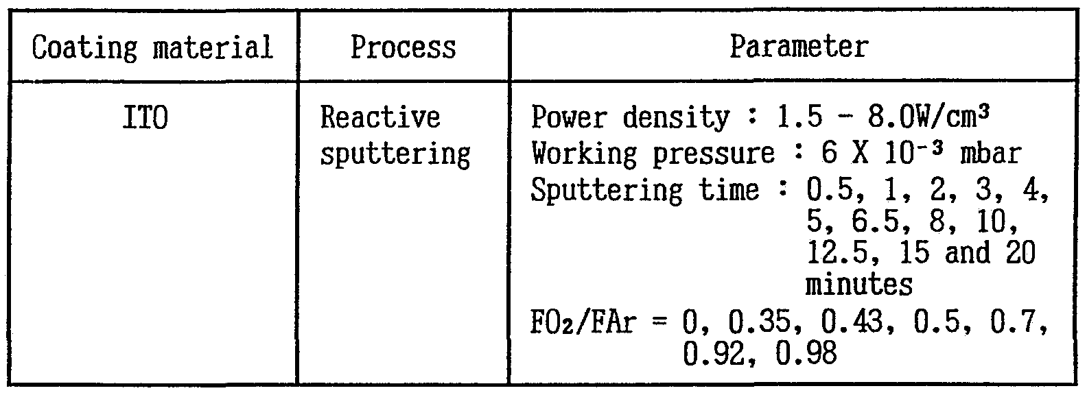
- the density of the electric power can be 1.5 - 8.0W/cm 3 and if it is higher, it takes short time for the vacuum evaporation and if it is lower, it takes long time for it. It is more desirable to set the density of the power at 2.26W/cm 3 and the time at 6.5 minutes.
- the experimental conditions for said indium-tin oxide(ITO) are given in Table 1 below:
- coating layers is Au with the best conductivity, and in the present invention Au
- Fig. 3 is a graph to show the different transparencies of the ITO and Au thin coating layers obtained by varied times of vacuum evaporation.
- the penetration of light was about 80% when the thin coating layer's thickness was 0.8 /im.vacuum evaporation by sputtering for 6.5 minutes), and the transparency gradually decreased as the layer's thickness
- the resistive features were measured by calculating the current, as 10V electric pressure was applied, after placing a Cu electrode each on both ends of
- Fig. 4(A) carries a graph showing the resistive features of an ITO experimental piece, different as the time for vacuum evaporation by the
- the value of resistance was 400 ⁇ when the time for vacuum evaporation by the sputtering was two minutes, but it declined rapidly as the time was protracted to fall, for instance, as low as about 20 ⁇ when the time was
- Fig. 4(B) carries a graph of the resistive features in the case of an Au coating layer, and in this, too, as in the case of the ITO coating layer, the resistance rapidly declined with rapidity as the time for vacuum ' evaporation by the sputtering increased.
- the object of the present invention is to develop a material as well as the software for the manufacture of conductive and transparent glass for use in automobiles, and since the change of temperatures of the experimental piece makes, as well as its transparency, a most important part of the present invention, the temperatures should be measured acculately.
- a K-type thermo-electric band was attached by means of silver paste and it was connected to a X-Y recorder in order to measure continuously the temperatures of the surface of the experimental piece varying at the change of the electric pressure and the electric current.
- Fig. 5(A) is a graph showing the measured surface temperatures of the ITO thin
- the 110 thin coating of 6,000A having, as shown in Fig. 3, a transparency of 80%, it can be adopted as a very important material in production of the conductive glass for automobiles.
- Fig. 5(B) shows the curve indicating the surface temperatures of the Au thin
- coating layers of 400A in thickness the electric current being 0.114A when it was supplied at 13.8V, the surface temperature showing about 45 * C 600 seconds later.
- Fig. 6 shows the results of XRD analysis of the ITO experimental piece with its FO ⁇ /EAr value at 0.43, wherein in the case of an experimental piece of good transparency and conductivity its In ⁇ SnOs coating exceedingly well develops at 2 ⁇ - 45.36, and it was found that the above ITO coating contributed to
- Such exothermic reflexible glass coated over the surface of the glass in automobiles, can be used very preferably to remove the moisture inside, and is extensively made use of for liquid crystal display systems also.
Landscapes
- Chemical & Material Sciences (AREA)
- Organic Chemistry (AREA)
- Engineering & Computer Science (AREA)
- Materials Engineering (AREA)
- Chemical Kinetics & Catalysis (AREA)
- Mechanical Engineering (AREA)
- Metallurgy (AREA)
- Life Sciences & Earth Sciences (AREA)
- General Chemical & Material Sciences (AREA)
- Geochemistry & Mineralogy (AREA)
- Inorganic Chemistry (AREA)
- Physical Vapour Deposition (AREA)
- Surface Treatment Of Glass (AREA)
Abstract
Description

Claims
Priority Applications (3)
| Application Number | Priority Date | Filing Date | Title |
|---|---|---|---|
| JP5511286A JPH07509534A (en) | 1991-12-28 | 1992-12-28 | Heat-generating reflective glass, heat-generating transparent glass, and manufacturing methods thereof |
| RU9294033355A RU2075537C1 (en) | 1992-12-05 | 1992-12-28 | Exothermic glass and methods of its production |
| EP93901531A EP0618984A1 (en) | 1991-12-28 | 1992-12-28 | Exothermic reflexible glass, exothermic transparent glass and process of manufacturing them |
Applications Claiming Priority (4)
| Application Number | Priority Date | Filing Date | Title |
|---|---|---|---|
| KR1991-24856 | 1991-12-28 | ||
| KR910024856 | 1991-12-28 | ||
| KR920023423 | 1992-12-05 | ||
| KR1992-23423 | 1992-12-05 |
Publications (1)
| Publication Number | Publication Date |
|---|---|
| WO1993013239A1 true WO1993013239A1 (en) | 1993-07-08 |
Family
ID=26628884
Family Applications (1)
| Application Number | Title | Priority Date | Filing Date |
|---|---|---|---|
| PCT/KR1992/000081 Ceased WO1993013239A1 (en) | 1991-12-28 | 1992-12-28 | Exothermic reflexible glass, exothermic transparent glass and process of manufacturing them |
Country Status (4)
| Country | Link |
|---|---|
| EP (1) | EP0618984A1 (en) |
| JP (1) | JPH07509534A (en) |
| CA (1) | CA2126674A1 (en) |
| WO (1) | WO1993013239A1 (en) |
Citations (3)
| Publication number | Priority date | Publication date | Assignee | Title |
|---|---|---|---|---|
| EP0293645A1 (en) * | 1987-06-04 | 1988-12-07 | Siemens Aktiengesellschaft | Process for the fabrication of transparent, conductive indium-tinoxide layers, especially for image sensor lines based on amorphous silicon |
| DE3933713A1 (en) * | 1988-10-08 | 1990-04-12 | Matsushita Electric Works Ltd | METHOD FOR FORMING A CONDUCTIVE METAL LAYER ON AN INORGANIC SUBSTRATE |
| EP0447850A2 (en) * | 1990-02-27 | 1991-09-25 | Nihon Shinku Gijutsu Kabushiki Kaisha | Method and apparatus for producing transparent conductive film |
-
1992
- 1992-12-28 EP EP93901531A patent/EP0618984A1/en not_active Withdrawn
- 1992-12-28 CA CA 2126674 patent/CA2126674A1/en not_active Abandoned
- 1992-12-28 JP JP5511286A patent/JPH07509534A/en active Pending
- 1992-12-28 WO PCT/KR1992/000081 patent/WO1993013239A1/en not_active Ceased
Patent Citations (3)
| Publication number | Priority date | Publication date | Assignee | Title |
|---|---|---|---|---|
| EP0293645A1 (en) * | 1987-06-04 | 1988-12-07 | Siemens Aktiengesellschaft | Process for the fabrication of transparent, conductive indium-tinoxide layers, especially for image sensor lines based on amorphous silicon |
| DE3933713A1 (en) * | 1988-10-08 | 1990-04-12 | Matsushita Electric Works Ltd | METHOD FOR FORMING A CONDUCTIVE METAL LAYER ON AN INORGANIC SUBSTRATE |
| EP0447850A2 (en) * | 1990-02-27 | 1991-09-25 | Nihon Shinku Gijutsu Kabushiki Kaisha | Method and apparatus for producing transparent conductive film |
Also Published As
| Publication number | Publication date |
|---|---|
| CA2126674A1 (en) | 1993-07-08 |
| JPH07509534A (en) | 1995-10-19 |
| EP0618984A1 (en) | 1994-10-12 |
Similar Documents
| Publication | Publication Date | Title |
|---|---|---|
| US3625848A (en) | Arc deposition process and apparatus | |
| US5009922A (en) | Method of forming a transparent conductive film | |
| US4006073A (en) | Thin film deposition by electric and magnetic crossed-field diode sputtering | |
| US4389299A (en) | Sputtering device | |
| US3756193A (en) | Coating apparatus | |
| Howson et al. | The formation and control of direct current magnetron discharges for the high‐rate reactive processing of thin films | |
| CN1101082A (en) | Anode structure for magnetron sputtering systems | |
| NL8200838A (en) | METHOD FOR APPLYING A LAYER BY CATHODE SPRAY AND APPARATUS FOR CARRYING OUT THIS METHOD | |
| US4209552A (en) | Thin film deposition by electric and magnetic crossed-field diode sputtering | |
| RU2075537C1 (en) | Exothermic glass and methods of its production | |
| US5427668A (en) | Thin film deposition system | |
| CN1174114C (en) | Bicathode-high frequency glow ion diffusion coating equipment and its process | |
| Williams | Vacuum coating with a hollow cathode source | |
| JPH02101160A (en) | Ion plating method | |
| WO1993013239A1 (en) | Exothermic reflexible glass, exothermic transparent glass and process of manufacturing them | |
| Karim et al. | Deposition of tin-doped indium oxide films by a modified reactive magnetron sputtering process | |
| US5597064A (en) | Electric contact materials, production methods thereof and electric contacts used these | |
| US3481854A (en) | Preparation of thin cermet films by radio frequency sputtering | |
| JPH11335815A (en) | Substrate with transparent conductive film and deposition apparatus | |
| KR20010005515A (en) | Magnesium oxide sputtering apparatus | |
| JPH03101033A (en) | Manufacture of thin film | |
| JP2002280171A (en) | Organic electroluminescence device and method of manufacturing the same | |
| KR900005841B1 (en) | High-hardness plating articles and method by a continous plating method using vaccum evaporation and aqueous solution | |
| JPH03232959A (en) | Production of thin film | |
| JP2633340B2 (en) | Method for forming transparent conductive film |
Legal Events
| Date | Code | Title | Description |
|---|---|---|---|
| AK | Designated states |
Kind code of ref document: A1 Designated state(s): CA FI HU JP RO RU US |
|
| AL | Designated countries for regional patents |
Kind code of ref document: A1 Designated state(s): AT BE CH DE DK ES FR GB GR IE IT LU MC NL PT SE |
|
| DFPE | Request for preliminary examination filed prior to expiration of 19th month from priority date (pct application filed before 20040101) | ||
| CFP | Corrected version of a pamphlet front page | ||
| CR1 | Correction of entry in section i |
Free format text: PAT.BUL.16/93, UNDER INID(51)"IPC",REPLACE"C23C 17/23"BY"C03C 17/23" |
|
| WWE | Wipo information: entry into national phase |
Ref document number: 2126674 Country of ref document: CA |
|
| WWE | Wipo information: entry into national phase |
Ref document number: 1993901531 Country of ref document: EP |
|
| WWP | Wipo information: published in national office |
Ref document number: 1993901531 Country of ref document: EP |
|
| WWW | Wipo information: withdrawn in national office |
Ref document number: 1993901531 Country of ref document: EP |
|
| EX32 | Extension under rule 32 effected after completion of technical preparation for international publication |
Free format text: AM+,KG+,MD+,TJ+,TM+ |