WO2000040402A1 - Layered product - Google Patents
Layered product Download PDFInfo
- Publication number
- WO2000040402A1 WO2000040402A1 PCT/JP1999/007344 JP9907344W WO0040402A1 WO 2000040402 A1 WO2000040402 A1 WO 2000040402A1 JP 9907344 W JP9907344 W JP 9907344W WO 0040402 A1 WO0040402 A1 WO 0040402A1
- Authority
- WO
- WIPO (PCT)
- Prior art keywords
- layer
- laminate
- visible light
- thickness
- titanium oxide
- Prior art date
- Legal status (The legal status is an assumption and is not a legal conclusion. Google has not performed a legal analysis and makes no representation as to the accuracy of the status listed.)
- Ceased
Links
Classifications
-
- C—CHEMISTRY; METALLURGY
- C03—GLASS; MINERAL OR SLAG WOOL
- C03C—CHEMICAL COMPOSITION OF GLASSES, GLAZES OR VITREOUS ENAMELS; SURFACE TREATMENT OF GLASS; SURFACE TREATMENT OF FIBRES OR FILAMENTS MADE FROM GLASS, MINERALS OR SLAGS; JOINING GLASS TO GLASS OR OTHER MATERIALS
- C03C17/00—Surface treatment of glass, not in the form of fibres or filaments, by coating
- C03C17/34—Surface treatment of glass, not in the form of fibres or filaments, by coating with at least two coatings having different compositions
- C03C17/36—Surface treatment of glass, not in the form of fibres or filaments, by coating with at least two coatings having different compositions at least one coating being a metal
- C03C17/3602—Surface treatment of glass, not in the form of fibres or filaments, by coating with at least two coatings having different compositions at least one coating being a metal the metal being present as a layer
- C03C17/3618—Coatings of type glass/inorganic compound/other inorganic layers, at least one layer being metallic
-
- B—PERFORMING OPERATIONS; TRANSPORTING
- B32—LAYERED PRODUCTS
- B32B—LAYERED PRODUCTS, i.e. PRODUCTS BUILT-UP OF STRATA OF FLAT OR NON-FLAT, e.g. CELLULAR OR HONEYCOMB, FORM
- B32B9/00—Layered products comprising a layer of a particular substance not covered by groups B32B11/00 - B32B29/00
- B32B9/04—Layered products comprising a layer of a particular substance not covered by groups B32B11/00 - B32B29/00 comprising such particular substance as the main or only constituent of a layer, which is next to another layer of the same or of a different material
-
- C—CHEMISTRY; METALLURGY
- C03—GLASS; MINERAL OR SLAG WOOL
- C03C—CHEMICAL COMPOSITION OF GLASSES, GLAZES OR VITREOUS ENAMELS; SURFACE TREATMENT OF GLASS; SURFACE TREATMENT OF FIBRES OR FILAMENTS MADE FROM GLASS, MINERALS OR SLAGS; JOINING GLASS TO GLASS OR OTHER MATERIALS
- C03C17/00—Surface treatment of glass, not in the form of fibres or filaments, by coating
- C03C17/34—Surface treatment of glass, not in the form of fibres or filaments, by coating with at least two coatings having different compositions
- C03C17/36—Surface treatment of glass, not in the form of fibres or filaments, by coating with at least two coatings having different compositions at least one coating being a metal
-
- C—CHEMISTRY; METALLURGY
- C03—GLASS; MINERAL OR SLAG WOOL
- C03C—CHEMICAL COMPOSITION OF GLASSES, GLAZES OR VITREOUS ENAMELS; SURFACE TREATMENT OF GLASS; SURFACE TREATMENT OF FIBRES OR FILAMENTS MADE FROM GLASS, MINERALS OR SLAGS; JOINING GLASS TO GLASS OR OTHER MATERIALS
- C03C17/00—Surface treatment of glass, not in the form of fibres or filaments, by coating
- C03C17/34—Surface treatment of glass, not in the form of fibres or filaments, by coating with at least two coatings having different compositions
- C03C17/36—Surface treatment of glass, not in the form of fibres or filaments, by coating with at least two coatings having different compositions at least one coating being a metal
- C03C17/3602—Surface treatment of glass, not in the form of fibres or filaments, by coating with at least two coatings having different compositions at least one coating being a metal the metal being present as a layer
- C03C17/3626—Surface treatment of glass, not in the form of fibres or filaments, by coating with at least two coatings having different compositions at least one coating being a metal the metal being present as a layer one layer at least containing a nitride, oxynitride, boronitride or carbonitride
-
- C—CHEMISTRY; METALLURGY
- C03—GLASS; MINERAL OR SLAG WOOL
- C03C—CHEMICAL COMPOSITION OF GLASSES, GLAZES OR VITREOUS ENAMELS; SURFACE TREATMENT OF GLASS; SURFACE TREATMENT OF FIBRES OR FILAMENTS MADE FROM GLASS, MINERALS OR SLAGS; JOINING GLASS TO GLASS OR OTHER MATERIALS
- C03C17/00—Surface treatment of glass, not in the form of fibres or filaments, by coating
- C03C17/34—Surface treatment of glass, not in the form of fibres or filaments, by coating with at least two coatings having different compositions
- C03C17/36—Surface treatment of glass, not in the form of fibres or filaments, by coating with at least two coatings having different compositions at least one coating being a metal
- C03C17/3602—Surface treatment of glass, not in the form of fibres or filaments, by coating with at least two coatings having different compositions at least one coating being a metal the metal being present as a layer
- C03C17/3634—Surface treatment of glass, not in the form of fibres or filaments, by coating with at least two coatings having different compositions at least one coating being a metal the metal being present as a layer one layer at least containing carbon, a carbide or oxycarbide
-
- C—CHEMISTRY; METALLURGY
- C03—GLASS; MINERAL OR SLAG WOOL
- C03C—CHEMICAL COMPOSITION OF GLASSES, GLAZES OR VITREOUS ENAMELS; SURFACE TREATMENT OF GLASS; SURFACE TREATMENT OF FIBRES OR FILAMENTS MADE FROM GLASS, MINERALS OR SLAGS; JOINING GLASS TO GLASS OR OTHER MATERIALS
- C03C17/00—Surface treatment of glass, not in the form of fibres or filaments, by coating
- C03C17/34—Surface treatment of glass, not in the form of fibres or filaments, by coating with at least two coatings having different compositions
- C03C17/36—Surface treatment of glass, not in the form of fibres or filaments, by coating with at least two coatings having different compositions at least one coating being a metal
- C03C17/3602—Surface treatment of glass, not in the form of fibres or filaments, by coating with at least two coatings having different compositions at least one coating being a metal the metal being present as a layer
- C03C17/3639—Multilayers containing at least two functional metal layers
-
- C—CHEMISTRY; METALLURGY
- C03—GLASS; MINERAL OR SLAG WOOL
- C03C—CHEMICAL COMPOSITION OF GLASSES, GLAZES OR VITREOUS ENAMELS; SURFACE TREATMENT OF GLASS; SURFACE TREATMENT OF FIBRES OR FILAMENTS MADE FROM GLASS, MINERALS OR SLAGS; JOINING GLASS TO GLASS OR OTHER MATERIALS
- C03C17/00—Surface treatment of glass, not in the form of fibres or filaments, by coating
- C03C17/34—Surface treatment of glass, not in the form of fibres or filaments, by coating with at least two coatings having different compositions
- C03C17/36—Surface treatment of glass, not in the form of fibres or filaments, by coating with at least two coatings having different compositions at least one coating being a metal
- C03C17/3602—Surface treatment of glass, not in the form of fibres or filaments, by coating with at least two coatings having different compositions at least one coating being a metal the metal being present as a layer
- C03C17/3642—Surface treatment of glass, not in the form of fibres or filaments, by coating with at least two coatings having different compositions at least one coating being a metal the metal being present as a layer the multilayer coating containing a metal layer
-
- C—CHEMISTRY; METALLURGY
- C03—GLASS; MINERAL OR SLAG WOOL
- C03C—CHEMICAL COMPOSITION OF GLASSES, GLAZES OR VITREOUS ENAMELS; SURFACE TREATMENT OF GLASS; SURFACE TREATMENT OF FIBRES OR FILAMENTS MADE FROM GLASS, MINERALS OR SLAGS; JOINING GLASS TO GLASS OR OTHER MATERIALS
- C03C17/00—Surface treatment of glass, not in the form of fibres or filaments, by coating
- C03C17/34—Surface treatment of glass, not in the form of fibres or filaments, by coating with at least two coatings having different compositions
- C03C17/36—Surface treatment of glass, not in the form of fibres or filaments, by coating with at least two coatings having different compositions at least one coating being a metal
- C03C17/3602—Surface treatment of glass, not in the form of fibres or filaments, by coating with at least two coatings having different compositions at least one coating being a metal the metal being present as a layer
- C03C17/3644—Surface treatment of glass, not in the form of fibres or filaments, by coating with at least two coatings having different compositions at least one coating being a metal the metal being present as a layer the metal being silver
-
- C—CHEMISTRY; METALLURGY
- C03—GLASS; MINERAL OR SLAG WOOL
- C03C—CHEMICAL COMPOSITION OF GLASSES, GLAZES OR VITREOUS ENAMELS; SURFACE TREATMENT OF GLASS; SURFACE TREATMENT OF FIBRES OR FILAMENTS MADE FROM GLASS, MINERALS OR SLAGS; JOINING GLASS TO GLASS OR OTHER MATERIALS
- C03C17/00—Surface treatment of glass, not in the form of fibres or filaments, by coating
- C03C17/34—Surface treatment of glass, not in the form of fibres or filaments, by coating with at least two coatings having different compositions
- C03C17/36—Surface treatment of glass, not in the form of fibres or filaments, by coating with at least two coatings having different compositions at least one coating being a metal
- C03C17/3602—Surface treatment of glass, not in the form of fibres or filaments, by coating with at least two coatings having different compositions at least one coating being a metal the metal being present as a layer
- C03C17/3657—Surface treatment of glass, not in the form of fibres or filaments, by coating with at least two coatings having different compositions at least one coating being a metal the metal being present as a layer the multilayer coating having optical properties
- C03C17/366—Low-emissivity or solar control coatings
-
- C—CHEMISTRY; METALLURGY
- C03—GLASS; MINERAL OR SLAG WOOL
- C03C—CHEMICAL COMPOSITION OF GLASSES, GLAZES OR VITREOUS ENAMELS; SURFACE TREATMENT OF GLASS; SURFACE TREATMENT OF FIBRES OR FILAMENTS MADE FROM GLASS, MINERALS OR SLAGS; JOINING GLASS TO GLASS OR OTHER MATERIALS
- C03C17/00—Surface treatment of glass, not in the form of fibres or filaments, by coating
- C03C17/34—Surface treatment of glass, not in the form of fibres or filaments, by coating with at least two coatings having different compositions
- C03C17/36—Surface treatment of glass, not in the form of fibres or filaments, by coating with at least two coatings having different compositions at least one coating being a metal
- C03C17/3602—Surface treatment of glass, not in the form of fibres or filaments, by coating with at least two coatings having different compositions at least one coating being a metal the metal being present as a layer
- C03C17/3668—Surface treatment of glass, not in the form of fibres or filaments, by coating with at least two coatings having different compositions at least one coating being a metal the metal being present as a layer the multilayer coating having electrical properties
- C03C17/3676—Surface treatment of glass, not in the form of fibres or filaments, by coating with at least two coatings having different compositions at least one coating being a metal the metal being present as a layer the multilayer coating having electrical properties specially adapted for use as electromagnetic shield
-
- C—CHEMISTRY; METALLURGY
- C23—COATING METALLIC MATERIAL; COATING MATERIAL WITH METALLIC MATERIAL; CHEMICAL SURFACE TREATMENT; DIFFUSION TREATMENT OF METALLIC MATERIAL; COATING BY VACUUM EVAPORATION, BY SPUTTERING, BY ION IMPLANTATION OR BY CHEMICAL VAPOUR DEPOSITION, IN GENERAL; INHIBITING CORROSION OF METALLIC MATERIAL OR INCRUSTATION IN GENERAL
- C23C—COATING METALLIC MATERIAL; COATING MATERIAL WITH METALLIC MATERIAL; SURFACE TREATMENT OF METALLIC MATERIAL BY DIFFUSION INTO THE SURFACE, BY CHEMICAL CONVERSION OR SUBSTITUTION; COATING BY VACUUM EVAPORATION, BY SPUTTERING, BY ION IMPLANTATION OR BY CHEMICAL VAPOUR DEPOSITION, IN GENERAL
- C23C14/00—Coating by vacuum evaporation, by sputtering or by ion implantation of the coating forming material
- C23C14/06—Coating by vacuum evaporation, by sputtering or by ion implantation of the coating forming material characterised by the coating material
-
- C—CHEMISTRY; METALLURGY
- C23—COATING METALLIC MATERIAL; COATING MATERIAL WITH METALLIC MATERIAL; CHEMICAL SURFACE TREATMENT; DIFFUSION TREATMENT OF METALLIC MATERIAL; COATING BY VACUUM EVAPORATION, BY SPUTTERING, BY ION IMPLANTATION OR BY CHEMICAL VAPOUR DEPOSITION, IN GENERAL; INHIBITING CORROSION OF METALLIC MATERIAL OR INCRUSTATION IN GENERAL
- C23C—COATING METALLIC MATERIAL; COATING MATERIAL WITH METALLIC MATERIAL; SURFACE TREATMENT OF METALLIC MATERIAL BY DIFFUSION INTO THE SURFACE, BY CHEMICAL CONVERSION OR SUBSTITUTION; COATING BY VACUUM EVAPORATION, BY SPUTTERING, BY ION IMPLANTATION OR BY CHEMICAL VAPOUR DEPOSITION, IN GENERAL
- C23C14/00—Coating by vacuum evaporation, by sputtering or by ion implantation of the coating forming material
- C23C14/06—Coating by vacuum evaporation, by sputtering or by ion implantation of the coating forming material characterised by the coating material
- C23C14/08—Oxides
- C23C14/083—Oxides of refractory metals or yttrium
-
- C—CHEMISTRY; METALLURGY
- C23—COATING METALLIC MATERIAL; COATING MATERIAL WITH METALLIC MATERIAL; CHEMICAL SURFACE TREATMENT; DIFFUSION TREATMENT OF METALLIC MATERIAL; COATING BY VACUUM EVAPORATION, BY SPUTTERING, BY ION IMPLANTATION OR BY CHEMICAL VAPOUR DEPOSITION, IN GENERAL; INHIBITING CORROSION OF METALLIC MATERIAL OR INCRUSTATION IN GENERAL
- C23C—COATING METALLIC MATERIAL; COATING MATERIAL WITH METALLIC MATERIAL; SURFACE TREATMENT OF METALLIC MATERIAL BY DIFFUSION INTO THE SURFACE, BY CHEMICAL CONVERSION OR SUBSTITUTION; COATING BY VACUUM EVAPORATION, BY SPUTTERING, BY ION IMPLANTATION OR BY CHEMICAL VAPOUR DEPOSITION, IN GENERAL
- C23C14/00—Coating by vacuum evaporation, by sputtering or by ion implantation of the coating forming material
- C23C14/06—Coating by vacuum evaporation, by sputtering or by ion implantation of the coating forming material characterised by the coating material
- C23C14/14—Metallic material, boron or silicon
- C23C14/18—Metallic material, boron or silicon on other inorganic substrates
- C23C14/185—Metallic material, boron or silicon on other inorganic substrates by cathodic sputtering
-
- C—CHEMISTRY; METALLURGY
- C23—COATING METALLIC MATERIAL; COATING MATERIAL WITH METALLIC MATERIAL; CHEMICAL SURFACE TREATMENT; DIFFUSION TREATMENT OF METALLIC MATERIAL; COATING BY VACUUM EVAPORATION, BY SPUTTERING, BY ION IMPLANTATION OR BY CHEMICAL VAPOUR DEPOSITION, IN GENERAL; INHIBITING CORROSION OF METALLIC MATERIAL OR INCRUSTATION IN GENERAL
- C23C—COATING METALLIC MATERIAL; COATING MATERIAL WITH METALLIC MATERIAL; SURFACE TREATMENT OF METALLIC MATERIAL BY DIFFUSION INTO THE SURFACE, BY CHEMICAL CONVERSION OR SUBSTITUTION; COATING BY VACUUM EVAPORATION, BY SPUTTERING, BY ION IMPLANTATION OR BY CHEMICAL VAPOUR DEPOSITION, IN GENERAL
- C23C28/00—Coating for obtaining at least two superposed coatings either by methods not provided for in a single one of groups C23C2/00 - C23C26/00 or by combinations of methods provided for in subclasses C23C and C25C or C25D
-
- C—CHEMISTRY; METALLURGY
- C23—COATING METALLIC MATERIAL; COATING MATERIAL WITH METALLIC MATERIAL; CHEMICAL SURFACE TREATMENT; DIFFUSION TREATMENT OF METALLIC MATERIAL; COATING BY VACUUM EVAPORATION, BY SPUTTERING, BY ION IMPLANTATION OR BY CHEMICAL VAPOUR DEPOSITION, IN GENERAL; INHIBITING CORROSION OF METALLIC MATERIAL OR INCRUSTATION IN GENERAL
- C23C—COATING METALLIC MATERIAL; COATING MATERIAL WITH METALLIC MATERIAL; SURFACE TREATMENT OF METALLIC MATERIAL BY DIFFUSION INTO THE SURFACE, BY CHEMICAL CONVERSION OR SUBSTITUTION; COATING BY VACUUM EVAPORATION, BY SPUTTERING, BY ION IMPLANTATION OR BY CHEMICAL VAPOUR DEPOSITION, IN GENERAL
- C23C28/00—Coating for obtaining at least two superposed coatings either by methods not provided for in a single one of groups C23C2/00 - C23C26/00 or by combinations of methods provided for in subclasses C23C and C25C or C25D
- C23C28/30—Coatings combining at least one metallic layer and at least one inorganic non-metallic layer
- C23C28/32—Coatings combining at least one metallic layer and at least one inorganic non-metallic layer including at least one pure metallic layer
- C23C28/321—Coatings combining at least one metallic layer and at least one inorganic non-metallic layer including at least one pure metallic layer with at least one metal alloy layer
-
- C—CHEMISTRY; METALLURGY
- C23—COATING METALLIC MATERIAL; COATING MATERIAL WITH METALLIC MATERIAL; CHEMICAL SURFACE TREATMENT; DIFFUSION TREATMENT OF METALLIC MATERIAL; COATING BY VACUUM EVAPORATION, BY SPUTTERING, BY ION IMPLANTATION OR BY CHEMICAL VAPOUR DEPOSITION, IN GENERAL; INHIBITING CORROSION OF METALLIC MATERIAL OR INCRUSTATION IN GENERAL
- C23C—COATING METALLIC MATERIAL; COATING MATERIAL WITH METALLIC MATERIAL; SURFACE TREATMENT OF METALLIC MATERIAL BY DIFFUSION INTO THE SURFACE, BY CHEMICAL CONVERSION OR SUBSTITUTION; COATING BY VACUUM EVAPORATION, BY SPUTTERING, BY ION IMPLANTATION OR BY CHEMICAL VAPOUR DEPOSITION, IN GENERAL
- C23C28/00—Coating for obtaining at least two superposed coatings either by methods not provided for in a single one of groups C23C2/00 - C23C26/00 or by combinations of methods provided for in subclasses C23C and C25C or C25D
- C23C28/30—Coatings combining at least one metallic layer and at least one inorganic non-metallic layer
- C23C28/32—Coatings combining at least one metallic layer and at least one inorganic non-metallic layer including at least one pure metallic layer
- C23C28/322—Coatings combining at least one metallic layer and at least one inorganic non-metallic layer including at least one pure metallic layer only coatings of metal elements only
-
- C—CHEMISTRY; METALLURGY
- C23—COATING METALLIC MATERIAL; COATING MATERIAL WITH METALLIC MATERIAL; CHEMICAL SURFACE TREATMENT; DIFFUSION TREATMENT OF METALLIC MATERIAL; COATING BY VACUUM EVAPORATION, BY SPUTTERING, BY ION IMPLANTATION OR BY CHEMICAL VAPOUR DEPOSITION, IN GENERAL; INHIBITING CORROSION OF METALLIC MATERIAL OR INCRUSTATION IN GENERAL
- C23C—COATING METALLIC MATERIAL; COATING MATERIAL WITH METALLIC MATERIAL; SURFACE TREATMENT OF METALLIC MATERIAL BY DIFFUSION INTO THE SURFACE, BY CHEMICAL CONVERSION OR SUBSTITUTION; COATING BY VACUUM EVAPORATION, BY SPUTTERING, BY ION IMPLANTATION OR BY CHEMICAL VAPOUR DEPOSITION, IN GENERAL
- C23C28/00—Coating for obtaining at least two superposed coatings either by methods not provided for in a single one of groups C23C2/00 - C23C26/00 or by combinations of methods provided for in subclasses C23C and C25C or C25D
- C23C28/30—Coatings combining at least one metallic layer and at least one inorganic non-metallic layer
- C23C28/34—Coatings combining at least one metallic layer and at least one inorganic non-metallic layer including at least one inorganic non-metallic material layer, e.g. metal carbide, nitride, boride, silicide layer and their mixtures, enamels, phosphates and sulphates
-
- C—CHEMISTRY; METALLURGY
- C23—COATING METALLIC MATERIAL; COATING MATERIAL WITH METALLIC MATERIAL; CHEMICAL SURFACE TREATMENT; DIFFUSION TREATMENT OF METALLIC MATERIAL; COATING BY VACUUM EVAPORATION, BY SPUTTERING, BY ION IMPLANTATION OR BY CHEMICAL VAPOUR DEPOSITION, IN GENERAL; INHIBITING CORROSION OF METALLIC MATERIAL OR INCRUSTATION IN GENERAL
- C23C—COATING METALLIC MATERIAL; COATING MATERIAL WITH METALLIC MATERIAL; SURFACE TREATMENT OF METALLIC MATERIAL BY DIFFUSION INTO THE SURFACE, BY CHEMICAL CONVERSION OR SUBSTITUTION; COATING BY VACUUM EVAPORATION, BY SPUTTERING, BY ION IMPLANTATION OR BY CHEMICAL VAPOUR DEPOSITION, IN GENERAL
- C23C28/00—Coating for obtaining at least two superposed coatings either by methods not provided for in a single one of groups C23C2/00 - C23C26/00 or by combinations of methods provided for in subclasses C23C and C25C or C25D
- C23C28/30—Coatings combining at least one metallic layer and at least one inorganic non-metallic layer
- C23C28/34—Coatings combining at least one metallic layer and at least one inorganic non-metallic layer including at least one inorganic non-metallic material layer, e.g. metal carbide, nitride, boride, silicide layer and their mixtures, enamels, phosphates and sulphates
- C23C28/341—Coatings combining at least one metallic layer and at least one inorganic non-metallic layer including at least one inorganic non-metallic material layer, e.g. metal carbide, nitride, boride, silicide layer and their mixtures, enamels, phosphates and sulphates with at least one carbide layer
-
- C—CHEMISTRY; METALLURGY
- C23—COATING METALLIC MATERIAL; COATING MATERIAL WITH METALLIC MATERIAL; CHEMICAL SURFACE TREATMENT; DIFFUSION TREATMENT OF METALLIC MATERIAL; COATING BY VACUUM EVAPORATION, BY SPUTTERING, BY ION IMPLANTATION OR BY CHEMICAL VAPOUR DEPOSITION, IN GENERAL; INHIBITING CORROSION OF METALLIC MATERIAL OR INCRUSTATION IN GENERAL
- C23C—COATING METALLIC MATERIAL; COATING MATERIAL WITH METALLIC MATERIAL; SURFACE TREATMENT OF METALLIC MATERIAL BY DIFFUSION INTO THE SURFACE, BY CHEMICAL CONVERSION OR SUBSTITUTION; COATING BY VACUUM EVAPORATION, BY SPUTTERING, BY ION IMPLANTATION OR BY CHEMICAL VAPOUR DEPOSITION, IN GENERAL
- C23C28/00—Coating for obtaining at least two superposed coatings either by methods not provided for in a single one of groups C23C2/00 - C23C26/00 or by combinations of methods provided for in subclasses C23C and C25C or C25D
- C23C28/30—Coatings combining at least one metallic layer and at least one inorganic non-metallic layer
- C23C28/34—Coatings combining at least one metallic layer and at least one inorganic non-metallic layer including at least one inorganic non-metallic material layer, e.g. metal carbide, nitride, boride, silicide layer and their mixtures, enamels, phosphates and sulphates
- C23C28/345—Coatings combining at least one metallic layer and at least one inorganic non-metallic layer including at least one inorganic non-metallic material layer, e.g. metal carbide, nitride, boride, silicide layer and their mixtures, enamels, phosphates and sulphates with at least one oxide layer
- C23C28/3455—Coatings combining at least one metallic layer and at least one inorganic non-metallic layer including at least one inorganic non-metallic material layer, e.g. metal carbide, nitride, boride, silicide layer and their mixtures, enamels, phosphates and sulphates with at least one oxide layer with a refractory ceramic layer, e.g. refractory metal oxide, ZrO2, rare earth oxides or a thermal barrier system comprising at least one refractory oxide layer
-
- C—CHEMISTRY; METALLURGY
- C23—COATING METALLIC MATERIAL; COATING MATERIAL WITH METALLIC MATERIAL; CHEMICAL SURFACE TREATMENT; DIFFUSION TREATMENT OF METALLIC MATERIAL; COATING BY VACUUM EVAPORATION, BY SPUTTERING, BY ION IMPLANTATION OR BY CHEMICAL VAPOUR DEPOSITION, IN GENERAL; INHIBITING CORROSION OF METALLIC MATERIAL OR INCRUSTATION IN GENERAL
- C23C—COATING METALLIC MATERIAL; COATING MATERIAL WITH METALLIC MATERIAL; SURFACE TREATMENT OF METALLIC MATERIAL BY DIFFUSION INTO THE SURFACE, BY CHEMICAL CONVERSION OR SUBSTITUTION; COATING BY VACUUM EVAPORATION, BY SPUTTERING, BY ION IMPLANTATION OR BY CHEMICAL VAPOUR DEPOSITION, IN GENERAL
- C23C28/00—Coating for obtaining at least two superposed coatings either by methods not provided for in a single one of groups C23C2/00 - C23C26/00 or by combinations of methods provided for in subclasses C23C and C25C or C25D
- C23C28/40—Coatings including alternating layers following a pattern, a periodic or defined repetition
- C23C28/42—Coatings including alternating layers following a pattern, a periodic or defined repetition characterized by the composition of the alternating layers
-
- G—PHYSICS
- G02—OPTICS
- G02B—OPTICAL ELEMENTS, SYSTEMS OR APPARATUS
- G02B5/00—Optical elements other than lenses
- G02B5/20—Filters
- G02B5/28—Interference filters
- G02B5/281—Interference filters designed for the infrared light
- G02B5/282—Interference filters designed for the infrared light reflecting for infrared and transparent for visible light, e.g. heat reflectors, laser protection
-
- C—CHEMISTRY; METALLURGY
- C03—GLASS; MINERAL OR SLAG WOOL
- C03C—CHEMICAL COMPOSITION OF GLASSES, GLAZES OR VITREOUS ENAMELS; SURFACE TREATMENT OF GLASS; SURFACE TREATMENT OF FIBRES OR FILAMENTS MADE FROM GLASS, MINERALS OR SLAGS; JOINING GLASS TO GLASS OR OTHER MATERIALS
- C03C2217/00—Coatings on glass
- C03C2217/70—Properties of coatings
- C03C2217/78—Coatings specially designed to be durable, e.g. scratch-resistant
-
- C—CHEMISTRY; METALLURGY
- C03—GLASS; MINERAL OR SLAG WOOL
- C03C—CHEMICAL COMPOSITION OF GLASSES, GLAZES OR VITREOUS ENAMELS; SURFACE TREATMENT OF GLASS; SURFACE TREATMENT OF FIBRES OR FILAMENTS MADE FROM GLASS, MINERALS OR SLAGS; JOINING GLASS TO GLASS OR OTHER MATERIALS
- C03C2217/00—Coatings on glass
- C03C2217/90—Other aspects of coatings
- C03C2217/94—Transparent conductive oxide layers [TCO] being part of a multilayer coating
- C03C2217/948—Layers comprising indium tin oxide [ITO]
-
- Y—GENERAL TAGGING OF NEW TECHNOLOGICAL DEVELOPMENTS; GENERAL TAGGING OF CROSS-SECTIONAL TECHNOLOGIES SPANNING OVER SEVERAL SECTIONS OF THE IPC; TECHNICAL SUBJECTS COVERED BY FORMER USPC CROSS-REFERENCE ART COLLECTIONS [XRACs] AND DIGESTS
- Y10—TECHNICAL SUBJECTS COVERED BY FORMER USPC
- Y10T—TECHNICAL SUBJECTS COVERED BY FORMER US CLASSIFICATION
- Y10T428/00—Stock material or miscellaneous articles
- Y10T428/12—All metal or with adjacent metals
- Y10T428/12493—Composite; i.e., plural, adjacent, spatially distinct metal components [e.g., layers, joint, etc.]
- Y10T428/12771—Transition metal-base component
- Y10T428/12861—Group VIII or IB metal-base component
- Y10T428/12889—Au-base component
-
- Y—GENERAL TAGGING OF NEW TECHNOLOGICAL DEVELOPMENTS; GENERAL TAGGING OF CROSS-SECTIONAL TECHNOLOGIES SPANNING OVER SEVERAL SECTIONS OF THE IPC; TECHNICAL SUBJECTS COVERED BY FORMER USPC CROSS-REFERENCE ART COLLECTIONS [XRACs] AND DIGESTS
- Y10—TECHNICAL SUBJECTS COVERED BY FORMER USPC
- Y10T—TECHNICAL SUBJECTS COVERED BY FORMER US CLASSIFICATION
- Y10T428/00—Stock material or miscellaneous articles
- Y10T428/12—All metal or with adjacent metals
- Y10T428/12493—Composite; i.e., plural, adjacent, spatially distinct metal components [e.g., layers, joint, etc.]
- Y10T428/12771—Transition metal-base component
- Y10T428/12861—Group VIII or IB metal-base component
- Y10T428/12896—Ag-base component
-
- Y—GENERAL TAGGING OF NEW TECHNOLOGICAL DEVELOPMENTS; GENERAL TAGGING OF CROSS-SECTIONAL TECHNOLOGIES SPANNING OVER SEVERAL SECTIONS OF THE IPC; TECHNICAL SUBJECTS COVERED BY FORMER USPC CROSS-REFERENCE ART COLLECTIONS [XRACs] AND DIGESTS
- Y10—TECHNICAL SUBJECTS COVERED BY FORMER USPC
- Y10T—TECHNICAL SUBJECTS COVERED BY FORMER US CLASSIFICATION
- Y10T428/00—Stock material or miscellaneous articles
- Y10T428/12—All metal or with adjacent metals
- Y10T428/12493—Composite; i.e., plural, adjacent, spatially distinct metal components [e.g., layers, joint, etc.]
- Y10T428/12771—Transition metal-base component
- Y10T428/12861—Group VIII or IB metal-base component
- Y10T428/12903—Cu-base component
-
- Y—GENERAL TAGGING OF NEW TECHNOLOGICAL DEVELOPMENTS; GENERAL TAGGING OF CROSS-SECTIONAL TECHNOLOGIES SPANNING OVER SEVERAL SECTIONS OF THE IPC; TECHNICAL SUBJECTS COVERED BY FORMER USPC CROSS-REFERENCE ART COLLECTIONS [XRACs] AND DIGESTS
- Y10—TECHNICAL SUBJECTS COVERED BY FORMER USPC
- Y10T—TECHNICAL SUBJECTS COVERED BY FORMER US CLASSIFICATION
- Y10T428/00—Stock material or miscellaneous articles
- Y10T428/26—Web or sheet containing structurally defined element or component, the element or component having a specified physical dimension
- Y10T428/263—Coating layer not in excess of 5 mils thick or equivalent
- Y10T428/264—Up to 3 mils
- Y10T428/265—1 mil or less
Definitions
- the present invention relates to a laminate having a titanium oxide layer and a method for producing the same.
- a laminate in which a metal layer is laminated on a transparent substrate such as glass (hereinafter, referred to as a “metal-containing laminate”) is used for the purpose of suppressing radiation of heat rays and reducing the load of cooling and heating. Widely used for windowpanes of automobiles and automobiles.
- the metal-containing laminate is also used as a shielding material for suppressing leakage of electromagnetic waves radiated from various devices such as plasma displays.
- the metal-containing laminate When the metal-containing laminate is applied to window glass or the like, it is required to reduce the emission of heat rays and to have a high visible light transmittance, and at the same time, to have a low visible light reflectance and a favorable reflection color tone.
- the metal-containing laminate when used as an electromagnetic wave shielding material, it is required to have not only high conductivity, but also high visible light transmittance and low visible light reflectance as much as possible, and more preferable reflection color tone.
- c low in order to obtain a high visible light transmittance, c low is known that laminate film formed by laminating alternately a dielectric layer and a metal layer are preferred hot wire Only emissivity (ie high conductivity) can be obtained by thickening the metal layer. This causes a decrease in visible light transmittance and an increase in visible light reflectance. In addition, since the wavelength band in which a low reflectance is obtained in the visible light region is narrowed, a preferable reflection color tone is impaired.
- the wavelength width at which a low reflectance is obtained in the visible light region is broadened compared to the case where a material having a lower refractive index than titanium oxide is used. And a more favorable reflection color tone can be obtained.
- the visible light transmittance was reduced due to this force, and the reduction rate of the visible light transmittance was increased as the number of layers increased.
- An object of the present invention is to improve the transmittance in the visible region of a laminate using titanium oxide.
- Another object of the present invention is to improve the scratch resistance of a laminate using titanium oxide. Disclosure of the invention
- the present invention provides a laminate in which a titanium oxide layer, a metal layer, a titanium oxide layer, and a force are alternately laminated in this order on a substrate, and 2 n + l (n is a positive integer) layers, Provided is a laminate in which an intermediate layer having a refractive index of less than 2.4 at a wavelength of 550 nm is interposed in at least one of the layers between the oxide layer and the metal layer.
- the present invention provides a method for producing a laminate in which a titanium oxide layer, a metal layer, and a titanium oxide layer are alternately laminated on a base in an order of 2 n + 1 (n is a positive integer).
- a method for producing a laminate having a step of interposing an intermediate layer having a refractive index of less than 2.4 at a wavelength of 550 nm in at least one layer between a titanium oxide layer and a metal layer.
- FIG. 1 is a schematic cross-sectional view showing the layer structure of the laminate manufactured in Examples 1 to 5, 18 to 19, 63 to 68, and 81 to 89.
- FIG. 2 is a schematic cross-sectional view illustrating a layer configuration of the laminate manufactured in Comparative Example 1.
- FIG. 3 shows Examples 6 to 12, 20 to 21, 69 to 72, 90 to 100, 122 to 1
- FIG. 26 is a schematic cross-sectional view showing a layer configuration of a laminate manufactured in 26, and 127 to 1331.
- FIG. 4 is a schematic cross-sectional view showing the layer structure of the laminate manufactured in Examples 13 to 17 and 73 to 80.
- FIG. 5 is a schematic cross-sectional view showing the layer configuration of the laminates manufactured in Comparative Examples 2 and 3.
- FIG. 6 is a schematic cross-sectional view showing the layer configuration of the laminates manufactured in Comparative Examples 4 and 5.
- FIG. 7 is a diagram showing the relationship between the thickness of the intermediate layer and the visible light transmittance of the laminates manufactured in Examples 1 to 17.
- FIG. 8 is a diagram showing the visible spectral characteristics of the laminates manufactured in Examples 1 and 2 and Comparative Example 1.
- FIG. 9 is a diagram showing visible spectral characteristics of the laminates manufactured in Examples 6 and 8 and Comparative Example 1.
- FIG. 10 is a diagram showing the visible spectral characteristics of the laminates manufactured in Examples 13 to 15 and Comparative Example 1.
- FIG. 11 is a schematic cross-sectional view showing the layer structure of the laminate manufactured in Examples 22 to 23 and 101 to 102 of the present invention.
- FIG. 12 is a schematic cross-sectional view showing the layer configuration of the laminate manufactured in Comparative Example 6.
- FIG. 13 is a schematic cross-sectional view showing the layer structure of the laminate manufactured in Examples 24 to 25 and 103 to 104.
- FIG. 14 is a schematic cross-sectional view showing the layer structure of the laminate manufactured in Examples 26 to 27 and 105 to 106.
- FIG. 15 is a schematic cross-sectional view showing the layer configuration of the laminate manufactured in Examples 28 to 29 and 107 to 108.
- FIG. 16 is a schematic cross-sectional view showing the layer structure of the laminate manufactured in Examples 30 to 31 and 109 to 110.
- FIG. 17 is a schematic cross-sectional view showing a layer configuration of the laminate manufactured in Examples 32 to 33 and 11 to 11.
- FIG. 18 is a schematic cross-sectional view showing the layer configuration of the laminate manufactured in Examples 34 to 35 and 113 to 114.
- FIG. 19 shows the layer structure of the laminate manufactured in Examples 36 to 37 and 115 to 116.
- FIG. 20 is a schematic cross-sectional view showing the layer configuration of the laminate manufactured in Examples 3840 and 117-121.
- FIG. 21 is a diagram showing the visible spectral characteristics of the laminates manufactured in Example 380 and Comparative Example 6.
- FIG. 22 is a schematic cross-sectional view illustrating a layer configuration of the laminated body manufactured in Example 41
- FIG. 23 is a schematic cross-sectional view illustrating a layer configuration of the laminated body manufactured in Example 43. is there.
- FIG. 24 is a schematic cross-sectional view illustrating the layer configuration of the laminate manufactured in Comparative Example 7.
- FIG. 25 is a schematic cross-sectional view illustrating the layer configuration of the laminate manufactured in Example 44.
- FIG. 26 is a schematic cross-sectional view showing the layer configuration of the laminate manufactured in Example 45.
- FIG. 27 is a schematic cross-sectional view illustrating a layer configuration of the laminate manufactured in Examples 46 to 47.
- FIG. 28 illustrates a layer configuration of the laminate manufactured in Examples 48 to 54.
- FIG. 29 is a schematic cross-sectional view ( FIG. 29 is a schematic cross-sectional view illustrating a layer configuration of a laminate manufactured in Comparative Example 9).
- FIG. 30 is a diagram showing the relationship between the visible light transmittance and the sheet resistance of the laminates manufactured in Examples 48 to 50 and Comparative Examples 9 to 11.
- FIG. 31 is a diagram showing the relationship between the visible light reflectance and the sheet resistance of the laminates manufactured in Examples 48 to 50 and Comparative Examples 9 to 11.
- FIG. 32 is a schematic cross-sectional view showing a layer structure of the laminate manufactured in Examples 55 to 57
- FIG. 33 is a cross-sectional view of the laminate manufactured in Examples 55 to 57 and Comparative Examples 12 to 14
- FIG. 7 is a view showing a relationship between a visible light transmittance and a sheet resistance value in a laminated body.
- FIG. 34 is a diagram showing the relationship between the visible light reflectance and the sheet resistance of the laminates manufactured in Examples 55 to 57 and Comparative Examples 12 to 14. BEST MODE FOR CARRYING OUT THE INVENTION
- the metal layer and the titanium oxide layer are alternately laminated in a pair on the first titanium oxide layer on the substrate side. Only one pair of the metal layer and the titanium oxide layer may be stacked, or a plurality of pairs may be stacked.
- the laminate of the present invention may have a layer configuration in which a metal layer and a titanium oxide layer are each laminated only one layer on the first layer, or on the first layer, It may have a layer configuration in which a plurality of layers are alternately stacked in the order of a metal layer and a titanium oxide layer.
- the substrate is not particularly limited.
- window glass made of soda lime glass, netted glass, frosted glass, etc.
- window glass for vehicles such as automobiles, 3) PET, etc.
- Plastic films made of acrylic resin, etc., 5) glass, plastic films and plastic plates used for displays.
- a transparent substrate is preferable.
- Each titanium oxide layer in the laminate of the present invention is preferably a layer having a refractive index at a wavelength of 550 nm of 2.4 or more, and may be composed of only a titanium oxide (titania), A small amount of other elemental components other than titanium may be included. Examples of the other element components include Nb, Cr, Zr, and the like.
- the thickness of the first layer on the substrate side and the thickness of the titanium oxide layer farthest from the substrate are preferably from 20 to 60 nm, particularly from 25 to 4 nm. 5 nm is preferred.
- the thickness of the titanium oxide layer other than the first layer and the titanium oxide layer farthest from the substrate is preferably 40 to 120 nm, particularly preferably 50 to 90 nm, and visible. From the viewpoint of reducing the light reflectivity and broadening the wavelength band in which a low reflectivity can be obtained.
- the first layer and the titanium oxide layer farthest from the substrate are thinner than the other titanium oxide layers. (Especially a thickness of about 1/2).
- the plurality of titanium oxide layers may have the same composition as each other or may have different compositions.
- the metal layer has at least one selected from silver, copper and gold. It is preferable that the layer contains a kind of metal. Silver, copper, gold or alloys containing these as main components may be used.
- alloys containing silver, copper or gold as main components include: 1) a silver Pd alloy containing Pd at 5.0 atomic% or less (preferably in the range of 0.1 to 3 atomic ° / 0 ) 2) silver containing at Au a 5.0 atomic% or less (preferably 0.1 to 3 atomic% range) - gold alloy, or 3) (1 and ⁇ :? each 0.5 to 3 atomic 0 / Examples include silver Pd—Cu alloys that are included in the range of 0. Note that the above content ratio is a ratio to the total amount with silver, and will be used in the same meaning hereinafter.
- each metal layer may be a layer having the same composition or a layer having a different composition.
- the thickness of the metal layer is preferably from 8 to 30 nm. From the viewpoint of reducing the visible light reflectance and broadening the wavelength band in which a low reflectance can be obtained, the thickness of the metal layer closest to the base and the thickness of the metal layer furthest from the base are the same as those of the other metal layers. It is preferably 0.5 to 1.0 times.
- the total thickness is preferably 120 nm or less.
- the number of metal layers is two when the target of the resistance value of the obtained laminate is 2.
- the target of the resistance value is 1.5 ⁇ / b
- the target of the resistance value is 0.5
- a plurality of intermediate layers may be provided, or may be provided above and below the metal layer with the metal layer interposed therebetween. In particular, it is preferable because all the metal layers are sandwiched between the two intermediate layers and have the highest visible light transmittance.
- a configuration in which an intermediate layer force s is provided above the metal layer is preferable in terms of excellent scratch resistance.
- the abrasion resistance is lower than when an intermediate layer is provided above the metal layer closest to the base.
- the intermediate layer may be made of any material as long as the refractive index at a wavelength of 550 nm is less than 2.4. In particular, a material made of a material having a refractive index of 1.6 to 2.39 is preferable.
- the intermediate layer is preferably a layer made of at least one selected from oxides, nitrides, oxynitrides, carbides and borides. Specific examples of the material constituting the intermediate layer include silicon nitride (refractive index: 2.0), niobium oxide (refractive index: 2.35), zinc oxide (refractive index: 2.0), and oxide. Tin (refractive index: 2.0).
- the intermediate layer is not intended to improve the visible light transmittance by the optical interference effect, and the intermediate layer is effective even if the thickness is smaller than the thickness causing the optical interference effect.
- the intermediate layer suppresses the generation of surface plasmons at the interface between the metal layer and the titanium oxide layer, thereby suppressing the loss of visible light in the laminate caused by light absorption by surface plasmons.
- the upper limit of the thickness of the intermediate layer is 30 nm, especially 10 nm. nm, preferably 5 nm.
- the upper limit of the thickness of the intermediate layer is preferably 20 nm, particularly preferably 15 nm.
- the lower limit of the thickness of the intermediate layer is preferably 0.1 nm, particularly preferably 0.5 nm.
- the total thickness is preferably 40 nm or less.
- the laminate of the present invention has high conductivity, it has electromagnetic wave shielding performance. Further, since it has a high reflectance in the near-infrared region, it also has near-infrared shielding performance.
- the transmittance at a wavelength of 900 nm is preferably 15% or less.
- the laminate of the present invention has a sheet resistance of 0.5 to 3.5 ⁇ and a visible light transmittance of 4
- the visible light reflectance is 0% or more and 10% or less.
- the laminate of the present invention preferably has an emissivity of 0.08 or less.
- Electromagnetic waves radiated from an electromagnetic wave source such as a plasma display using the laminate of the present invention It is also preferable to use it for the purpose of suppressing the leakage of water.
- the laminate of the present invention preferably has an electromagnetic wave shielding factor at 30 ° z of 10 db or more, particularly preferably 15 db or more, and further preferably 17 db or more. If the sheet resistance value is the same, the electromagnetic shielding factor will be almost the same.
- the laminate of the present invention when used for an application that emphasizes low reflection performance, it is preferable to laminate a resin film having further low reflection performance on the laminate, and to reduce the visible light reflectance to 3% or less. be able to.
- the laminate of the present invention When the laminate of the present invention is used for applications that emphasize near-infrared shielding performance, it is preferable to further laminate a resin film having near-infrared shielding performance, and to reduce the transmittance at a wavelength of 900 nm by 5%. % Or less.
- the resin film is bonded 1) on the multilayer film of the laminate of the present invention, and Z or 2) on the substrate surface opposite to the substrate surface on which the laminate of the present invention is formed.
- the resin film having low reflection performance examples include a resin film formed of urethane, PET, or the like, on which an antireflection layer is formed.
- the resin film has low reflection performance and also has scattering prevention performance.
- the antireflection layer 1) a non-crystal properties of the fluoropolymer (e.g., Asahi Glass Co. site top) made of a low refractive index layer. 2) Low consisting S i 0 2, M g F 2 etc. Refractive index layers, 3) multilayer films in which low refractive index layers and high refractive index layers are alternately stacked, 4) porous silica films, and the like.
- Examples of the resin film having near-infrared shielding performance include those obtained by mixing a near-infrared absorbing agent into a resin film made of urethane, PET, or the like. Further, a near-infrared absorbing agent may be mixed into the adhesive layer used for bonding.
- the titanium oxide layer is formed by, for example, a method of forming by a direct current sputtering method using a reducing target of titanium oxide, a reactive sputtering method, an ion plating method, and a vapor deposition method. It can be formed according to the CVD method.
- the method of forming by a DC sputtering method using a reducing target of titanium oxide can prevent oxidation of the metal layer when forming the titanium oxide layer on the metal layer, and has a high speed and a large area. This is advantageous in that it can be formed uniformly.
- the reducing target of titanium oxide is a target that is deficient in oxygen relative to the stoichiometric composition of titanium oxide. Specifically, it is preferable to use one having a composition represented by the formula of TiO x (1 ⁇ x ⁇ 2). Titanium oxide reducing targets can be prepared, for example, by using titania powder or a mixture of titania powder and titanium powder as a raw material described in International Publication It can be manufactured by the joining method or the thermal spraying method.
- 0. 1 is preferred to use an inert gas containing 1 0 vol 0/0 of an oxidizing gas.
- the use of an inert gas containing an oxidizing gas having a concentration in this range as a sputtering gas is effective in suppressing the oxidation of the metal layer when forming the titanium oxide layer, and has a low emissivity and high conductivity. This is effective in that a laminated body having the following can be manufactured. Especially 0.1 to 5 volumes. It is preferable to use an inert gas containing an oxidizing gas of / 0 .
- oxygen gas can be generally used, but nitric oxide, nitrogen dioxide, carbon monoxide, carbon dioxide, ozone and the like can also be used.
- the metal layer can be formed according to various methods such as a sputtering method, a CVD method, and a vapor deposition method.
- a sputtering method a sputtering method
- CVD method a vapor deposition method
- the formation of the intermediate layer can be performed according to a method appropriately selected according to the composition of the layer to be formed.
- a method such as a sputtering method, a CVD method, and an evaporation method.
- a direct current sputtering method is preferable.
- the laminate of the present invention includes a heat-shielding article (for example, a heat-shielding window glass), an optical filter (for example, a near-infrared shielding filter installed on the front of the PDP), and an electromagnetic wave-shielding article (for example, an electromagnetic wave shielding plate installed on the front of the PDP).
- a heat-shielding article for example, a heat-shielding window glass
- an optical filter for example, a near-infrared shielding filter installed on the front of the PDP
- an electromagnetic wave-shielding article for example, an electromagnetic wave shielding plate installed on the front of the PDP.
- the spectral transmittance and the spectral reflectance at a wavelength of three hundred forty to seven hundred eighty nm was measured, in conformity with JISR 3 1 06, against the CIE standard illuminant D 65 as defined in JISZ 8720, visible by the spectral luminous efficiency of CIE light adaptation
- the hemispherical emissivity and the hemispherical value are measured using a SCALING DEGITAL VOLTMETER (commonly known as an emissomiter) manufactured by Devices & Services. The correction coefficient between and was determined in advance.
- the emisomitter values of the samples obtained in the examples and comparative examples were measured, and the hemispherical emissivity was determined by multiplying the emisomitter value by the correction coefficient.
- the pencil scratch value was measured under a load of 1 kg according to JIS K 5400, and the measured value was used as an index of scratch resistance.
- a metal layer made of silver containing 1 atomic% of Pd (hereinafter simply referred to as “Ag Pd layer) (14 nm thick).
- the content of palladium in the target is the ratio to the total amount with silver, and will be used in the same meaning hereinafter.
- Si area: 432 mm X 127 mm
- Example X the laminate obtained in Example X is referred to as “laminate A-X”.
- titania layer 2 have A g _ 1 at% P d layer 3 have S i N x interlayer 4 2 and titania Tier 5! Are laminated.
- 1 is a source one da-lime glass, 2, titania layer, 3, 3 2, 3 3, 3 4, A g -! Lat% P d layer, have 4 12, 4 21, 4 22, 4 31, 4 32, 4, 4 42, an intermediate layer, 5 had 5 2, 5 3, 5 4, titania layer, 6, a top coat layer, 7 is a bottom coat layer, 8, resin Film.
- Table 1 shows the visible light transmittance, visible light reflectance, sheet resistance, and emissivity of the laminate A-1.
- Example 2 As shown in FIG. 2 in the same manner as in Example 1 except that the SiN x intermediate layer 4 12 was not formed, a 33-nm-thick titania layer 2 j and a thickness 14 were formed on soda-lime glass 1.
- the laminate obtained in Comparative Example Y is referred to as “laminate BY”.
- Table 1 shows the visible light transmittance, the visible light reflectance, the sheet resistance, and the emissivity of the obtained laminated body II-1.
- Laminates A-2 to A-17 and Laminates B-2 to B-5 were produced.
- the laminates A—2 to A—5 were successively formed on a soda lime glass 1 in the order of a titania layer 2 Ag—1 at% Pd layer 3 S i N x intermediate layer 4 j and titania layer 5 have a laminated structure.
- the laminates A-6 to A-12 (Examples 6 to 12) On Mugarasu 1, sequentially, titania layer 2,, S i N x intermediate layer 4, A g - with 1 at% P d layer 3, and a titania layer 5] force s stacked configuration.
- the laminates A—13 to A—17 were sequentially formed on a soda lime glass 1 by a titania layer 2 or a SiN x intermediate layer 4. ! , Ag—1 at% Pd layer 3, a S i N x intermediate layer 4 i 2, and a titania layer 5, which are stacked.
- the laminates ⁇ -2 and ⁇ -3 (Comparative Examples 2 and 3) were successively provided with a titania layer 2 ⁇ Ag—lat% Pd layer 3 ⁇ titania on soda lime glass 1. It has a configuration in which a layer 5, and a top coat layer 6 made of SiN x are laminated. As shown in FIG.
- the laminates B—4 and B_5 (Comparative Examples 4 and 5) were sequentially coated on a soda-lime glass 1 with a bottom coat layer 7 composed of SiN x and a titania layer 2A. g-1 at% Pd layer 3 and titania layer 5 are laminated.
- the top coat layer consisting of S i N x it has displaced the bottom coat layer consisting of S i N x was also formed by the same forming method as S i x interlayer.
- FIG. 8 shows the visible spectral characteristics of the laminates A-1 and A-2 together with the visible spectral characteristics of the laminate B-1.
- FIG. 9 shows the visible spectral characteristics of the laminates A-6 and A-8 together with the visible spectral characteristics of the laminate B-1.
- FIG. 10 shows the visible spectral characteristics of the laminates A-13, A-14 and A-15, together with the visible spectral characteristics of the laminate B-1.
- the top and bottom of the Ag—1 at% Pd layer The laminate having the configuration including the S i N x intermediate layer exhibited higher visible light transmittance than the laminate having the configuration including the intermediate layer only above or below the Ag-1 at% Pd layer.
- the visible light transmittance is about 3% higher than that of the laminate B-1 having no intermediate layer.
- the thickness of the Six intermediate layer is effective at 0.5 nm, and the effect does not depend on the film thickness.
- the bottom coat of SiN x before forming the first titania layer and the top coat of SiN x of the uppermost layer have almost no effect of improving the transmittance.
- the resulting laminates A-18 to 21 were evaluated for scratch resistance. Also, the laminates obtained in Examples 12, 4, 5, 8, 11, and 12, and Comparative Example 1 were measured in the same manner. Table 3 shows the results.
- the index of scratch resistance was obtained for a laminate having a layer configuration in which a SiN x intermediate layer having a thickness of 0.5 nm or more was formed on the Ag-1at% Pd layer. It can be seen that the pencil scratch value is improved. In addition, even in a laminate having a layer structure in which a SiN x intermediate layer having a thickness of l nm or more is formed under the Ag—1 at% Pd layer, a pencil scratch, which is an indicator of scratch resistance, is used. It can be seen that the value improves.
- a laminate having a layer configuration in which an intermediate layer is formed on the Ag-lat% Pd layer has a greater effect of improving the pencil bow I grip value, and is obtained by increasing the thickness of the intermediate layer. It can be seen that the pencil draw value is further improved.
- Example 2 In the same manner as in Example 1, on the soda lime glass 1, a 33 nm-thick titanium layer 2), a 1 nm-thick SiN x intermediate layer 4! After laminating a 1411: 11 8-2—1 t% Pd layer 3, and a 66-nm-thick titania layer 5, a thickness of 1411111-8-1 at% P d layer 3 2, and a thickness of 3 3 nm titania layer 5 2 are laminated to produce a laminate A- 2 2 of the configuration shown in FIG 1.
- Table 4 (part 1) shows the visible light transmittance, the visible light reflectance, the sheet resistance, and the emissivity of the obtained laminate A-22.
- Table 4 shows the visible light transmittance, the visible light reflectance, the sheet resistance, and the emissivity of the obtained laminate B-6.
- the laminate A-23 (Example 23) is shown in FIG. 11, the laminates A-24 and A-25 (Examples 24 and 25) are shown in FIG. 13, and the laminates A-26 and A-27 is shown in Fig. 14, Laminate A-28 and A-29 are shown in Fig. 15, Laminate A- 30 and A-31 are shown in Fig. 16, Laminate A- 32 And A-33 in Figure 17; Laminates A-34 and A-35 in Figure 18; Laminates A-36 and A-37 in Figure 19; Laminates A-38 To A-40 have the configurations shown in FIG.
- FIG. 21 shows the visible spectral characteristics of the laminates A-38, A-39 and A-40, together with the visible spectral characteristics of the laminate B-6.
- the sheet resistance was measured before laminating the low-reflection resin film. The same applies to the following.
- the laminated body with the SiN x intermediate layer above and below each of the two Ag—1 at% Pd layers shows the highest visible light transmittance
- the comparative example 6 has the SiN x intermediate layer It shows about 6% higher visible light transmittance than the non-laminated laminate.
- the film thickness of the S i N x intermediate layer is effective in 1 nm, the effect does not depend on the film thickness.
- the transmittance of light at a wavelength of 900 nm and the electromagnetic wave shielding factor at a frequency of 3 OMHz were measured, and were 14.5% and 15 dB, respectively. From these results, it is clear that the laminate A-38 has good near-infrared shielding performance and electromagnetic wave shielding performance. It turns out that it has a function.
- Target made of silver containing 1 atomic 0/0 palladium (area 4 3 2 mmX 1 2 7 mm ) A g- 1 at% P d layer formed using a 1 atom 0/0 palladium Using a target made of silver containing 1 atomic% of copper (area: 432 mm x 127 mm), using argon gas as sputter gas and supplying 0.3 kW of power, Examples 38, 39, and 89 except for changing to a metal layer made of silver containing 1 at% 1!
- Laminates A—38a, A—39a, and A—40a were produced in the same manner as in Example 40.
- the obtained laminate was evaluated in the same manner as laminate A-38. The results are shown in Table 4 (part 3).
- the obtained laminate was evaluated in the same manner as in the laminate A-38. Table 4 shows the results.
- the laminate using the Ag-1at% Au layer In the laminate using the Ag-1at% Au layer, the same good result as the laminate using the Ag-1at% Pd layer can be obtained.
- the laminate using the Ag-1 at% Au layer has a larger thickness than the laminate using the Ag-1 at% Pd layer. Can obtain a high visible light transmittance of about 2%, and at the same time, a sheet resistance of about 10% lower when the thickness of the metal layer is the same.
- a low-refractive-index antireflection layer made of an amorphous fluoropolymer (Cytop, manufactured by Asahi Glass Co., Ltd.) is formed on one side of a polyurethane soft resin film (thickness: 200 m), and the other side is formed.
- a resin film having a low reflection performance with an acryl-based adhesive layer formed thereon (hereinafter referred to as a “low-reflection resin film”) was prepared.
- the visible light transmittance, the visible light reflectance, the transmittance of light having a wavelength of 900 nm, and the sheet resistance were measured in the same manner as in Example 38. Table 5 shows the results.
- Example 4 A near-infrared absorbing agent (SIR 159, manufactured by Mitsui Chemicals, Inc.) was added to the acrylic adhesive in an amount of 5% by weight based on the acrylic adhesive in the acryl adhesive layer of the low-reflection resin film used in Example 1.
- a resin film with near-infrared shielding as well as performance hereinafter referred to as “low-reflection near-infrared shielding resin film”.
- Example 41 the surface of the soda lime glass on the titania layer 52 of the laminate A-38 obtained in Example 38 and on the side opposite to the side on which the laminated film was laminated. Then, a low-reflection near-infrared shielding resin film was bonded to each of them to produce a laminate A-42.
- the obtained laminate A-42 was measured in the same manner as in Example 38. The results are shown in Table 5.From the results shown in Table 5, 74% or more was obtained by laminating the low-reflection resin film. It can be seen that the visible light reflectance can be suppressed to less than 2% while the visible light transmittance of the laminated body can be suppressed to less than 2%, and further excellent low reflection performance can be obtained.
- the transmittance of light at a wavelength of 900 nm can be suppressed to 5% or less without deteriorating good optical characteristics in the visible light region. It can be seen that a better near-infrared shielding performance than that of the laminate A-38 was obtained.
- Table 6 shows the results of evaluation of the scratch resistance of the laminates A-24, 25, 28, 29, 32, and 33 and the laminate B-6.
- each layer laminate structure shown in Table 7 A- 4 3 c obtained laminate was produced A- 4 3 visible light transmittance, visible light reflectance, the sheet Table 7 shows the resistance values.
- a laminate B-7 having the layer configuration shown in FIG. 24 and each layer having the configuration shown in Table 7 was produced in the same manner as in Example 43 except that no intermediate layer was provided.
- Table 7 shows the visible light transmittance, the visible light reflectance, and the sheet resistance of the obtained laminate B-7.
- Example 43 In the same manner as in Example 43, a laminate A-44 having the layer configuration shown in FIG. 25 (Example 44) and FIG. 26 (Example 45) and each layer having the configuration shown in Table 7 And 45 were manufactured ( measurement results of the visible light transmittance, the visible light reflectance, and the sheet resistance of the obtained laminates A—44 and 45 together with the results of Example 43) are shown in Table 7. Shown in
- the intermediate layer is interposed between the SiN layers and the (2n + 1) layer is a seven-layer laminate.
- Laminate A-46 was manufactured by laminating low-reflective resin film 8.
- Table 8 shows the visible light transmittance, the visible light reflectance, the sheet resistance, and the transmittance of light having a wavelength of 900 nm of the obtained laminate A-46.
- a laminate A-47 was manufactured by laminating a low-reflection near-infrared shielding resin film, respectively.
- the obtained laminate A-47 was measured in the same manner as in Example 46.
- Table 8 shows the results. As shown in Table 8, by laminating the low-reflection resin film, the visible light reflectance can be suppressed to less than 2% while obtaining the visible light transmittance of 67% or more. It can be seen that even better low reflection performance can be obtained.
- Table 9 shows the visible light transmittance, the visible light reflectance, and the sheet resistance of the obtained laminate A-48.
- a laminate B-9 having the layer configuration shown in FIG. 29 and each layer having the configuration shown in Table 9 was produced in the same manner as in Example 48.
- Table 9 shows the visible light transmittance, the visible light reflectance, and the sheet resistance of the obtained laminate B-9.
- titania layer except for changing the thickness of the S i x interlayer or A g- 1 at% P d layer in the same manner as in Example 4 8, laminates A- 4 9 ⁇ A — The 54 was manufactured. Also, as shown in Table 9, laminated bodies B-10 to B-11 were produced in the same manner as in Comparative Example 9 except that the thickness of the titania layer or the Ag-1 at% Pd layer was changed. Table 9 shows the visible light transmittance, the visible light reflectance and the sheet resistance of the obtained laminates A-49 to A-54 and laminates B-10 to B-11.
- the thickness of the S i N x intermediate layer is 1 nm, and the effect is independent of the thickness of the S i N x intermediate layer.
- the laminate has a low sheet resistance of 0.5 to 0.9 ⁇ / s, a visible light transmittance of 40% or more and a visible light reflectance of 10% or less.
- an intermediate layer of SiN x is provided above and below the layer of Ag—1 at% Pd, and the (2 n + l) layer has nine layers. It can be seen that a laminate is preferable.
- the electromagnetic wave shielding ratio was over 17 db (about 20 db or more).
- a titania layer 5 4 on the laminate A- 48 obtained in Example 48, the surface of the source one da-lime glass on the side opposite to the stacked laminated film side, respectively low reaction Laminate A-55 was produced by laminating the sprayable resin film 8.
- Table 10 shows the visible light transmittance and the visible light reflectance of the obtained laminate A-55.
- the laminated body B of Comparative Examples 9 to 11 the titania layer 5 of 9 to 11 Laminates B-12 to 14 were produced by laminating low-reflection resin films, respectively.
- Table 10 shows the visible light transmittance, the visible light reflectance, and the sheet resistance of the obtained laminates A-55 to A-57 and laminates B-12 to B-14. The sheet resistance was measured before laminating the low-reflection resin film.
- FIG. 33 The relationship between the visible light transmittance and the sheet resistance for Examples 55 to 57 and Comparative Examples 12 to 14 is shown in FIG. 33, and the relationship between the visible light reflectance and the sheet resistance is shown in FIG. From the results shown in Fig. 33 and Fig. 34, it has a low sheet resistance value of 0.5 to 0.9 ⁇ , a visible light transmittance of 40% or more and a visible light reflectance of 3% or less.
- an intermediate layer of SiN x was provided, and an Ag—1 at% Pd layer and a titanium oxide layer were alternately formed. It can be seen that a layer configuration in which a low-reflection resin film is laminated on the titanium layer 54 and the soda lime glass substrate after laminating four layers each is preferred.
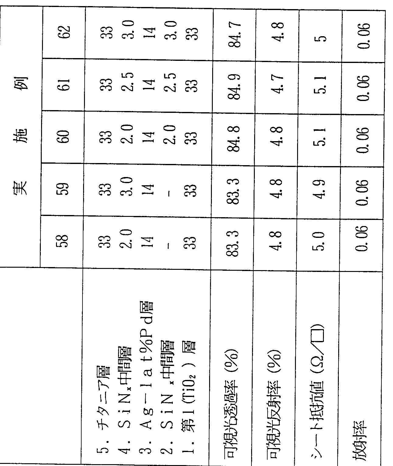
- each titania layer, T 1 Target have use (area 4 3 2 mmX 1 2 7mm) , the input power and 4 kW, using argon gas containing 50 vol 0/0 of the oxygen gas as a sputtering gas Laminates A-58 to A-62 were produced in the same manner as in Examples 13 to 17 except that the thickness of the SiN x intermediate layer was 1.0 to 3.0 nm. .
- the titania layer was formed using a ⁇ i target (area: 432 mm x 127 mm), input power of 4 kW, and argon gas containing 50% by volume of oxygen gas as sputtering gas.
- a laminate B-15 was produced in the same manner as in Comparative Example 1.
- Example 5 For the laminates A-58 to 62 and B-15 to 16 obtained in Examples 8 to 62 and Comparative Examples 15 to 16, the visible light transmittance and the visible light reflection were measured. Rate, sheet resistance and emissivity were measured. The results of Examples 58 to 62 are shown in Table 11, and the results of Comparative Examples 15 and 16 are shown in Table 12.
- the metal of the Ag-1 ato / o Pd layer was oxidized in the process of forming the titania layer, so that the resistance and the emissivity increased, and the conductivity was increased. And low radioactivity could not be obtained.
- the laminate B-16 obtained in Comparative Example 16 has a structure in which a titania layer is laminated on an Ag-1at% Pd layer via a Ti layer.
- a titania layer is laminated on an Ag-1at% Pd layer via a Ti layer.
- the finally obtained laminate B-16 has substantially the same layer configuration as the laminate B-1 without the intermediate layer obtained in Comparative Example 1.
- Laminate A-63 was obtained in the same manner as in Example 1, except that the formation of the intermediate layer was changed as described below.
- 7 wt% intermediate A layer hereinafter simply referred to as “GZO intermediate layer”) (refractive index: 2.0, thickness: 0.5 nm) was formed.
- the obtained laminate A-63 was placed on soda lime glass 1 in order, and the titania layer 2! , Ag- 1 at% P d layer 3 has a GZ_ ⁇ intermediate layer 4 12 and Chita two ⁇ layer 5] force stacked configuration.
- Table 13 shows the thickness of each layer.
- laminates A-64 to A-80 were produced in the same manner as in Example 63, except that the thickness or position of the GZ0 intermediate layer was changed.
- the case where the intermediate layer is disposed above and below the Ag-1 at% Pd layer shows the highest visible light transmittance, and the intermediate layer of Comparative Example 1 is not inserted. 3% higher visible light transmittance than The effect is seen when the thickness of the GZ0 intermediate layer is 0.5 nm, and the effect does not depend on the film thickness.
- Example 22 In the same manner as in Example 22 except that the intermediate layer was changed to a GZO intermediate layer, a 33 nm titania layer, a 1 nm GZO intermediate layer, and a 14 nm Ag—lat% P d were formed on soda lime glass. layer, titania layer of 66 nm, 1 4 nm of a g- 1 at% P d layer, sequentially forming a titania layer of 33 n m, laminate structure having Ag- 1 at% P d layer two layers A-101 was manufactured.
- laminates A-102 to A-121 were produced in the same manner as in Example 101 except that the thickness of the GZO intermediate layer or the position where the intermediate layer was formed was changed. Visible light transmittance, visible light reflectance, sheet resistance, and emissivity of the obtained laminates A-101-1 to A-1211 were measured. The results are shown in Table 15.
- GZ0 intermediate layers are formed above and below both the first and second Ag-1 at% Pd layers.
- the configuration in which the layers are arranged shows the highest visible light transmittance, and the visible light transmittance is about 7% higher than that of Comparative Example 6 where the intermediate layer is not inserted.
- the thickness of the GZO intermediate layer is effective at 0.5 nm and does not depend on the thickness.
- the obtained laminate A-122 is composed of a soda-lime glass 1, a titania layer, an intermediate layer composed of NbO x (hereinafter referred to as “NbO x intermediate layer”), and Ag-1at. / 0 Pd layer and a titania layer are laminated.
- Example 1 23 to 126 As shown in Table 1 6, to produce a Nb O x intermediate except that the thickness in the range of 1 to 4 nm in the same manner as in Example 1 22 stack of layers A- 1 23 ⁇ A- 1 26.
- Laminate having Nb_ ⁇ x interlayer below the A g- 1 at% P d layer exhibits about 5% high visible light transmittance 1. compared to have Comparative Example 1, such an intermediate layer.
- the thickness of the Nb O x intermediate layer is found effective in 0. 5 nm, the effect does not depend on the film thickness.
- Intermediate layer to obtain a S n 0 was changed to 2 comprises a layer in the same manner as in Example 6 laminate A- 1 27 including Injiumu below.
- Target consisting of S n 0 2 a includes 1 0 wt 0/0 Injiumu (area: 432 mmX 1 27 mm) using the argon gas as a sputtering gas, input power and lk W - containing 10% by weight of indium S intermediate layer of N_ ⁇ 2 (hereinafter, referred to as "I tO interlayer") (refractive index: 2. 0, l nm thickness) were formed.
- I tO interlayer indium S intermediate layer of N_ ⁇ 2
- laminated bodies A-128 to A-131 were manufactured in the same manner as in Example 127, except that the thickness of the ITO intermediate layer was changed in the range of 1.5 to 4 nm. did.
- the laminated body having the ITO intermediate layer under the Ag-1 at% Pd layer shows about 1.5% higher visible light transmittance than the laminated body without the intermediate layer of Comparative Example 1. .
- the effect is seen at a thickness of 1 nm for the I T0 intermediate layer, and the effect does not depend on the film thickness.
- permeability in the visible light region was improved is obtained.
- Titania 57 54 54 57 57 57 57 57 54 54
Landscapes
- Chemical & Material Sciences (AREA)
- Engineering & Computer Science (AREA)
- Organic Chemistry (AREA)
- Chemical Kinetics & Catalysis (AREA)
- Materials Engineering (AREA)
- Mechanical Engineering (AREA)
- Metallurgy (AREA)
- Life Sciences & Earth Sciences (AREA)
- Inorganic Chemistry (AREA)
- General Chemical & Material Sciences (AREA)
- Geochemistry & Mineralogy (AREA)
- Physics & Mathematics (AREA)
- Ceramic Engineering (AREA)
- General Physics & Mathematics (AREA)
- Optics & Photonics (AREA)
- Electromagnetism (AREA)
- Laminated Bodies (AREA)
Description




Claims
Priority Applications (3)
| Application Number | Priority Date | Filing Date | Title |
|---|---|---|---|
| DE69935166T DE69935166T2 (de) | 1998-12-28 | 1999-12-27 | Schichtprodukt |
| EP99961425A EP1155816B1 (en) | 1998-12-28 | 1999-12-27 | Layered product |
| US09/857,209 US7005189B1 (en) | 1998-12-28 | 1999-12-27 | Laminate and its production method |
Applications Claiming Priority (2)
| Application Number | Priority Date | Filing Date | Title |
|---|---|---|---|
| JP10/374186 | 1998-12-28 | ||
| JP37418698 | 1998-12-28 |
Publications (1)
| Publication Number | Publication Date |
|---|---|
| WO2000040402A1 true WO2000040402A1 (en) | 2000-07-13 |
Family
ID=18503415
Family Applications (1)
| Application Number | Title | Priority Date | Filing Date |
|---|---|---|---|
| PCT/JP1999/007344 Ceased WO2000040402A1 (en) | 1998-12-28 | 1999-12-27 | Layered product |
Country Status (7)
| Country | Link |
|---|---|
| US (1) | US7005189B1 (ja) |
| EP (1) | EP1155816B1 (ja) |
| KR (1) | KR100667637B1 (ja) |
| CN (1) | CN1145551C (ja) |
| DE (1) | DE69935166T2 (ja) |
| TW (1) | TW473434B (ja) |
| WO (1) | WO2000040402A1 (ja) |
Cited By (7)
| Publication number | Priority date | Publication date | Assignee | Title |
|---|---|---|---|---|
| US7771850B2 (en) * | 2003-08-25 | 2010-08-10 | Asahi Glass Company, Limited | Electromagnetic wave shielding laminate and display device employing it |
| US7972713B2 (en) * | 2003-11-28 | 2011-07-05 | Saint-Gobain Glass France | Transparent substrate which can be used alternatively or cumulatively for thermal control, electromagnetic armour and heated glazing |
| USRE43817E1 (en) | 2004-07-12 | 2012-11-20 | Cardinal Cg Company | Low-maintenance coatings |
| DE10196704B3 (de) * | 2000-09-29 | 2013-03-14 | Nippon Sheet Glass Co., Ltd. | Transparentes geschichtetes Erzeugnis mit einem Auftrag mit geringem Emissionsvermögen |
| US9663984B2 (en) | 2005-10-11 | 2017-05-30 | Cardinal Cg Company | High infrared reflection coatings, thin film coating deposition methods and associated technologies |
| US9738967B2 (en) | 2006-07-12 | 2017-08-22 | Cardinal Cg Company | Sputtering apparatus including target mounting and control |
| US10604442B2 (en) | 2016-11-17 | 2020-03-31 | Cardinal Cg Company | Static-dissipative coating technology |
Families Citing this family (35)
| Publication number | Priority date | Publication date | Assignee | Title |
|---|---|---|---|---|
| EP1539378A2 (en) * | 2002-09-19 | 2005-06-15 | Optimax Technology Corp. | Antiglare and antireflection coatings of surface active nanoparticles |
| KR20050084671A (ko) * | 2002-11-05 | 2005-08-26 | 엔.브이. 베카에르트 에스.에이. | 적외선 반사층 구조 |
| FR2869324B1 (fr) * | 2004-04-21 | 2007-08-10 | Saint Gobain | Procede de depot sous vide |
| JP2006186309A (ja) | 2004-11-30 | 2006-07-13 | Asahi Glass Co Ltd | 導電性積層体、プラズマディスプレイ用電磁波遮蔽フィルムおよびプラズマディスプレイ用保護板 |
| EP1860930A4 (en) * | 2005-02-25 | 2009-12-23 | Asahi Glass Co Ltd | ELECTROMAGNETIC SHIELDING LAMINATE AND DISPLAY THEREOF |
| US7572511B2 (en) | 2005-10-11 | 2009-08-11 | Cardinal Cg Company | High infrared reflection coatings |
| US7339728B2 (en) | 2005-10-11 | 2008-03-04 | Cardinal Cg Company | Low-emissivity coatings having high visible transmission and low solar heat gain coefficient |
| WO2007049478A1 (ja) * | 2005-10-26 | 2007-05-03 | Central Glass Company, Limited | 近赤外線反射基板およびその基板を用いた近赤外線反射合わせガラス、近赤外線反射複層ガラス |
| EP2013150B1 (en) | 2006-04-11 | 2018-02-28 | Cardinal CG Company | Photocatalytic coatings having improved low-maintenance properties |
| US7892662B2 (en) | 2006-04-27 | 2011-02-22 | Guardian Industries Corp. | Window with anti-bacterial and/or anti-fungal feature and method of making same |
| US7846492B2 (en) * | 2006-04-27 | 2010-12-07 | Guardian Industries Corp. | Photocatalytic window and method of making same |
| JP5023556B2 (ja) * | 2006-05-31 | 2012-09-12 | 旭硝子株式会社 | 導電性積層体、プラズマディスプレイ用電磁波遮蔽フィルムおよびプラズマディスプレイ用保護板 |
| US7820309B2 (en) | 2007-09-14 | 2010-10-26 | Cardinal Cg Company | Low-maintenance coatings, and methods for producing low-maintenance coatings |
| CN101971350B (zh) * | 2008-04-15 | 2012-10-10 | 株式会社爱发科 | 薄膜晶体管、薄膜晶体管的制造方法 |
| JPWO2010055832A1 (ja) * | 2008-11-11 | 2012-04-12 | 旭硝子株式会社 | 導電性積層体及びプラズマディスプレイ用保護板 |
| JP4858650B2 (ja) * | 2010-03-02 | 2012-01-18 | ソニー株式会社 | 光学体、窓材、建具および日射遮蔽装置 |
| US8574728B2 (en) | 2011-03-15 | 2013-11-05 | Kennametal Inc. | Aluminum oxynitride coated article and method of making the same |
| US10040719B2 (en) * | 2012-01-17 | 2018-08-07 | Cardinal Cg Company | Low solar transmittance coatings |
| US9138864B2 (en) | 2013-01-25 | 2015-09-22 | Kennametal Inc. | Green colored refractory coatings for cutting tools |
| US9017809B2 (en) | 2013-01-25 | 2015-04-28 | Kennametal Inc. | Coatings for cutting tools |
| US9427808B2 (en) | 2013-08-30 | 2016-08-30 | Kennametal Inc. | Refractory coatings for cutting tools |
| TWI700518B (zh) * | 2014-06-18 | 2020-08-01 | 美商唯亞威方案公司 | 金屬介電光學濾光器、感測器裝置及製造方法 |
| KR101991047B1 (ko) * | 2015-06-30 | 2019-06-19 | 주식회사 엘지화학 | 전도성 적층체, 이의 제조방법, 이를 포함하는 투명 전극 및 전자소자 |
| CN108455698B (zh) * | 2017-02-22 | 2020-12-25 | 南方科技大学 | 光催化组件及其制备方法 |
| US10556823B2 (en) | 2017-06-20 | 2020-02-11 | Apple Inc. | Interior coatings for glass structures in electronic devices |
| KR101922550B1 (ko) * | 2017-06-27 | 2018-11-27 | 주식회사 엘지화학 | 장식 부재 및 이의 제조방법 |
| US11192334B2 (en) * | 2017-06-27 | 2021-12-07 | Lg Chem, Ltd. | Decorative member and method for preparing same |
| US11345631B2 (en) * | 2017-09-08 | 2022-05-31 | Lg Hausys, Ltd. | Functional building material for door and window |
| US10611679B2 (en) | 2017-10-26 | 2020-04-07 | Guardian Glass, LLC | Coated article including noble metal and polymeric hydrogenated diamond like carbon composite material having antibacterial and photocatalytic properties, and/or methods of making the same |
| SE543408C2 (en) | 2018-10-22 | 2021-01-05 | Mimsi Mat Ab | Glazing and method of its production |
| JP7773370B2 (ja) * | 2020-04-06 | 2025-11-19 | 東レ株式会社 | 金属化フィルムおよびその製造方法 |
| WO2021214111A1 (en) * | 2020-04-21 | 2021-10-28 | Mimsi Materials Ab | Segmented planar sputtering target and methods for using the same |
| WO2021214109A1 (en) * | 2020-04-21 | 2021-10-28 | Mimsi Materials Ab | Solar control glazing and method of its production |
| WO2021214107A1 (en) | 2020-04-21 | 2021-10-28 | Mimsi Materials Ab | Solar control glazing and method of its production |
| WO2021214110A1 (en) * | 2020-04-21 | 2021-10-28 | Mimsi Materials Ab | Low-emissivity glazing and method of its production |
Citations (8)
| Publication number | Priority date | Publication date | Assignee | Title |
|---|---|---|---|---|
| JPS54127990A (en) * | 1978-03-29 | 1979-10-04 | Teijin Ltd | Laminate |
| JPS5511803A (en) * | 1978-07-11 | 1980-01-28 | Teijin Ltd | Stratified piece and making method thereof |
| JPH01128829A (ja) * | 1987-11-16 | 1989-05-22 | Nippon Sheet Glass Co Ltd | 反射防止膜付着透明板 |
| JPH01249330A (ja) * | 1988-03-30 | 1989-10-04 | Nippon Sheet Glass Co Ltd | 金属膜を含む反射防止膜付着透明体 |
| JPH03178430A (ja) * | 1989-03-07 | 1991-08-02 | Asahi Glass Co Ltd | 赤外反射物品 |
| JPH0743524A (ja) * | 1993-07-27 | 1995-02-14 | Central Glass Co Ltd | 紫外線熱線遮断ウィンドウ |
| JPH07138048A (ja) * | 1993-10-26 | 1995-05-30 | Nissan Motor Co Ltd | 紫外線熱線遮断ガラス |
| JPH07199812A (ja) * | 1993-12-28 | 1995-08-04 | Toppan Printing Co Ltd | 積層体 |
Family Cites Families (24)
| Publication number | Priority date | Publication date | Assignee | Title |
|---|---|---|---|---|
| US3962488A (en) * | 1974-08-09 | 1976-06-08 | Ppg Industries, Inc. | Electrically conductive coating |
| US4721349A (en) | 1974-08-16 | 1988-01-26 | Massachusetts Institute Of Technology | Transparent heat-mirror |
| DE3027256A1 (de) * | 1980-07-18 | 1982-02-18 | Robert Bosch Gmbh, 7000 Stuttgart | Mehrschichtsystem fuer waermeschutzanwendungen und verfahren zu seiner herstellung |
| US4379040A (en) | 1981-01-29 | 1983-04-05 | Ppg Industries, Inc. | Method of and apparatus for control of reactive sputtering deposition |
| US4565719A (en) * | 1982-10-08 | 1986-01-21 | Optical Coating Laboratory, Inc. | Energy control window film systems and methods for manufacturing the same |
| US4786783A (en) * | 1987-08-11 | 1988-11-22 | Monsanto Company | Electrically heatable laminated window |
| GB8900166D0 (en) | 1989-01-05 | 1989-03-01 | Glaverbel | Glass coating |
| JPH02225346A (ja) * | 1989-02-27 | 1990-09-07 | Central Glass Co Ltd | 熱線反射ガラス |
| IT1240796B (it) * | 1990-03-12 | 1993-12-17 | Siv Soc Italiana Vetro | Vetro per autoveicoli, atto ad essere usato come schermo solare e come combinatore di immagini. |
| JP3603315B2 (ja) * | 1993-02-19 | 2004-12-22 | 日本製紙株式会社 | 近赤外線吸収剤およびそれを含有した熱線遮蔽材 |
| FR2710333B1 (fr) * | 1993-09-23 | 1995-11-10 | Saint Gobain Vitrage Int | Substrat transparent muni d'un empilement de couches minces agissant sur le rayonnement solaire et/ou infra-rouge. |
| US5691044A (en) * | 1994-12-13 | 1997-11-25 | Asahi Glass Company, Ltd. | Light absorptive antireflector |
| FR2734811B1 (fr) | 1995-06-01 | 1997-07-04 | Saint Gobain Vitrage | Substrats transparents revetus d'un empilement de couches minces a proprietes de reflexion dans l'infrarouge et/ou dans le domaine du rayonnement solaire |
| US5719705A (en) | 1995-06-07 | 1998-02-17 | Sola International, Inc. | Anti-static anti-reflection coating |
| DE69737785T2 (de) * | 1996-04-18 | 2008-02-07 | Kanebo Trinity Holdings, Ltd. | Nahen infrarotstrahlen absorbierender film und damit ausgerüstete mehrschichtige verbrundplatte |
| JP3063618B2 (ja) | 1996-05-14 | 2000-07-12 | 凸版印刷株式会社 | 表示装置用電極基板 |
| TW415922B (en) | 1996-06-11 | 2000-12-21 | Asahi Glass Co Ltd | Light absorptive anti-reflector and method for manufacturing the same |
| FR2755962B1 (fr) * | 1996-11-21 | 1998-12-24 | Saint Gobain Vitrage | Vitrage comprenant un substrat muni d'un empilement de couches minces pour la protection solaire et/ou l'isolation thermique |
| DE69715567T3 (de) * | 1996-11-26 | 2016-08-04 | Saint-Gobain Glass France S.A. | Verwendung einer Verbundglasscheibe zur Dämmung von durch Festkörper geleiteten Schwingungen in einem Fahrzeug |
| FR2757151B1 (fr) * | 1996-12-12 | 1999-01-08 | Saint Gobain Vitrage | Vitrage comprenant un substrat muni d'un empilement de couches minces pour la protection solaire et/ou l'isolation thermique |
| JPH10278159A (ja) | 1997-04-08 | 1998-10-20 | Mitsui Chem Inc | 透明導電性薄膜積層体の製造方法 |
| JPH1164603A (ja) | 1997-08-18 | 1999-03-05 | Dainippon Printing Co Ltd | 反射防止膜と反射防止膜付き基材、および該反射防止膜付き基材を用いたプラズマディスプレイパネル前面板 |
| JP4066101B2 (ja) | 1997-10-17 | 2008-03-26 | 旭硝子株式会社 | 低放射率積層体の製造方法 |
| JPH11340678A (ja) | 1998-05-22 | 1999-12-10 | Teijin Ltd | 電磁波シールド用積層体 |
-
1999
- 1999-12-27 KR KR1020017008290A patent/KR100667637B1/ko not_active Expired - Fee Related
- 1999-12-27 WO PCT/JP1999/007344 patent/WO2000040402A1/ja not_active Ceased
- 1999-12-27 CN CNB998151343A patent/CN1145551C/zh not_active Expired - Fee Related
- 1999-12-27 DE DE69935166T patent/DE69935166T2/de not_active Expired - Lifetime
- 1999-12-27 EP EP99961425A patent/EP1155816B1/en not_active Expired - Lifetime
- 1999-12-27 US US09/857,209 patent/US7005189B1/en not_active Expired - Fee Related
- 1999-12-27 TW TW088123046A patent/TW473434B/zh not_active IP Right Cessation
Patent Citations (8)
| Publication number | Priority date | Publication date | Assignee | Title |
|---|---|---|---|---|
| JPS54127990A (en) * | 1978-03-29 | 1979-10-04 | Teijin Ltd | Laminate |
| JPS5511803A (en) * | 1978-07-11 | 1980-01-28 | Teijin Ltd | Stratified piece and making method thereof |
| JPH01128829A (ja) * | 1987-11-16 | 1989-05-22 | Nippon Sheet Glass Co Ltd | 反射防止膜付着透明板 |
| JPH01249330A (ja) * | 1988-03-30 | 1989-10-04 | Nippon Sheet Glass Co Ltd | 金属膜を含む反射防止膜付着透明体 |
| JPH03178430A (ja) * | 1989-03-07 | 1991-08-02 | Asahi Glass Co Ltd | 赤外反射物品 |
| JPH0743524A (ja) * | 1993-07-27 | 1995-02-14 | Central Glass Co Ltd | 紫外線熱線遮断ウィンドウ |
| JPH07138048A (ja) * | 1993-10-26 | 1995-05-30 | Nissan Motor Co Ltd | 紫外線熱線遮断ガラス |
| JPH07199812A (ja) * | 1993-12-28 | 1995-08-04 | Toppan Printing Co Ltd | 積層体 |
Non-Patent Citations (1)
| Title |
|---|
| See also references of EP1155816A4 * |
Cited By (13)
| Publication number | Priority date | Publication date | Assignee | Title |
|---|---|---|---|---|
| DE10196704B3 (de) * | 2000-09-29 | 2013-03-14 | Nippon Sheet Glass Co., Ltd. | Transparentes geschichtetes Erzeugnis mit einem Auftrag mit geringem Emissionsvermögen |
| US7771850B2 (en) * | 2003-08-25 | 2010-08-10 | Asahi Glass Company, Limited | Electromagnetic wave shielding laminate and display device employing it |
| US8440329B2 (en) | 2003-11-28 | 2013-05-14 | Saint-Gobain Glass France | Transparent substrate which can be used alternatively or cumulatively, for thermal control, for electromagnetic armour and for heated glazing |
| US7972713B2 (en) * | 2003-11-28 | 2011-07-05 | Saint-Gobain Glass France | Transparent substrate which can be used alternatively or cumulatively for thermal control, electromagnetic armour and heated glazing |
| US20110236663A1 (en) * | 2003-11-28 | 2011-09-29 | Saint-Gobain Glass France | Transparent substrate which can be used alternatively or cumulatively, for thermal control, for electromagnetic armour and for heated glazing |
| USRE43817E1 (en) | 2004-07-12 | 2012-11-20 | Cardinal Cg Company | Low-maintenance coatings |
| USRE44155E1 (en) | 2004-07-12 | 2013-04-16 | Cardinal Cg Company | Low-maintenance coatings |
| US9663984B2 (en) | 2005-10-11 | 2017-05-30 | Cardinal Cg Company | High infrared reflection coatings, thin film coating deposition methods and associated technologies |
| US10442728B2 (en) | 2005-10-11 | 2019-10-15 | Cardinal Cg Company | High infrared reflection coatings, thin film coating deposition methods and associated technologies |
| US11028011B2 (en) | 2005-10-11 | 2021-06-08 | Cardinal Cg Company | High infrared reflection coatings, thin film coating deposition methods and associated technologies |
| US9738967B2 (en) | 2006-07-12 | 2017-08-22 | Cardinal Cg Company | Sputtering apparatus including target mounting and control |
| US10604442B2 (en) | 2016-11-17 | 2020-03-31 | Cardinal Cg Company | Static-dissipative coating technology |
| US11325859B2 (en) | 2016-11-17 | 2022-05-10 | Cardinal Cg Company | Static-dissipative coating technology |
Also Published As
| Publication number | Publication date |
|---|---|
| CN1332672A (zh) | 2002-01-23 |
| EP1155816A4 (en) | 2003-05-14 |
| DE69935166T2 (de) | 2007-10-31 |
| CN1145551C (zh) | 2004-04-14 |
| US7005189B1 (en) | 2006-02-28 |
| EP1155816B1 (en) | 2007-02-14 |
| EP1155816A1 (en) | 2001-11-21 |
| TW473434B (en) | 2002-01-21 |
| DE69935166D1 (de) | 2007-03-29 |
| KR20010089736A (ko) | 2001-10-08 |
| KR100667637B1 (ko) | 2007-01-12 |
Similar Documents
| Publication | Publication Date | Title |
|---|---|---|
| WO2000040402A1 (en) | Layered product | |
| JP4370650B2 (ja) | 積層体およびその製造方法 | |
| EP3179283B1 (en) | Infrared-reflecting film | |
| JP4965254B2 (ja) | 反射防止膜を含む透明基板 | |
| EP1923362B1 (en) | Infrared reflective glass plate and laminated glass for vehicle window | |
| JP7656009B2 (ja) | 窒化ケイ素及び/又は酸窒化ケイ素を含む保護コーティングを有するコーティングされた物品 | |
| EP1923365A1 (en) | Laminated glass for vehicle window | |
| EP3179282A1 (en) | Infrared reflecting substrate | |
| EP2952939A1 (en) | Method for producing infrared radiation reflecting film | |
| CN1842503A (zh) | 有反射红外线和/或太阳辐射的多个薄层的叠层的玻璃板 | |
| JP2012037634A (ja) | 日射調整フィルムおよびこれを用いたフィルム付きガラス | |
| WO1998013850A1 (en) | Plasma display protective plate and its manufacturing method | |
| CN1639081A (zh) | 带有有耐磨耗性能的抗反射涂层的透明基底 | |
| CN101868346A (zh) | 电磁辐射屏蔽装置 | |
| EP2535180A1 (en) | Method for producing heat-shielding ply structure, heat-shielding ply structure, and transparent laminate film for ply structure | |
| JP2008037667A (ja) | 窓用合わせガラス | |
| WO2006090798A1 (ja) | 電磁波遮蔽積層体およびこれを用いたディスプレイ装置 | |
| EP2666757A1 (en) | Laminated glass and process for producing laminated glass | |
| JP4078520B2 (ja) | 表示装置用反射防止機能付フィルターの製造方法 | |
| WO2014050367A1 (ja) | 遮熱性合わせ構造体の製造方法、遮熱性合わせ構造体、透明積層フィルム | |
| JP4561995B2 (ja) | プラズマディスプレイパネル用フィルター及びプラズマディスプレイ装置 | |
| JP2011145443A (ja) | 光学物品およびその製造方法 | |
| JP5895089B1 (ja) | 熱線遮蔽積層体および該積層体を用いた窓ガラス | |
| JPWO1998013850A1 (ja) | プラズマディスプレイ用保護板とその製造方法 | |
| JP2008077102A (ja) | 表示装置用反射防止機能付フィルターの製造方法 |
Legal Events
| Date | Code | Title | Description |
|---|---|---|---|
| WWE | Wipo information: entry into national phase |
Ref document number: 99815134.3 Country of ref document: CN |
|
| AK | Designated states |
Kind code of ref document: A1 Designated state(s): CN KR US |
|
| AL | Designated countries for regional patents |
Kind code of ref document: A1 Designated state(s): AT BE CH CY DE DK ES FI FR GB GR IE IT LU MC NL PT SE |
|
| 121 | Ep: the epo has been informed by wipo that ep was designated in this application | ||
| DFPE | Request for preliminary examination filed prior to expiration of 19th month from priority date (pct application filed before 20040101) | ||
| WWE | Wipo information: entry into national phase |
Ref document number: 09857209 Country of ref document: US |
|
| WWE | Wipo information: entry into national phase |
Ref document number: 1020017008290 Country of ref document: KR |
|
| WWE | Wipo information: entry into national phase |
Ref document number: 1999961425 Country of ref document: EP |
|
| WWP | Wipo information: published in national office |
Ref document number: 1020017008290 Country of ref document: KR |
|
| WWP | Wipo information: published in national office |
Ref document number: 1999961425 Country of ref document: EP |
|
| WWG | Wipo information: grant in national office |
Ref document number: 1020017008290 Country of ref document: KR |
|
| WWG | Wipo information: grant in national office |
Ref document number: 1999961425 Country of ref document: EP |