WO2001084885A1 - Ceramic heater - Google Patents
Ceramic heater Download PDFInfo
- Publication number
- WO2001084885A1 WO2001084885A1 PCT/JP2001/003759 JP0103759W WO0184885A1 WO 2001084885 A1 WO2001084885 A1 WO 2001084885A1 JP 0103759 W JP0103759 W JP 0103759W WO 0184885 A1 WO0184885 A1 WO 0184885A1
- Authority
- WO
- WIPO (PCT)
- Prior art keywords
- heating element
- ceramic substrate
- ceramic
- weight
- resistance heating
- Prior art date
- Legal status (The legal status is an assumption and is not a legal conclusion. Google has not performed a legal analysis and makes no representation as to the accuracy of the status listed.)
- Ceased
Links
Classifications
-
- H—ELECTRICITY
- H10—SEMICONDUCTOR DEVICES; ELECTRIC SOLID-STATE DEVICES NOT OTHERWISE PROVIDED FOR
- H10P—GENERIC PROCESSES OR APPARATUS FOR THE MANUFACTURE OR TREATMENT OF DEVICES COVERED BY CLASS H10
- H10P72/00—Handling or holding of wafers, substrates or devices during manufacture or treatment thereof
- H10P72/04—Apparatus for manufacture or treatment
- H10P72/0431—Apparatus for thermal treatment
- H10P72/0434—Apparatus for thermal treatment mainly by convection
-
- H—ELECTRICITY
- H05—ELECTRIC TECHNIQUES NOT OTHERWISE PROVIDED FOR
- H05B—ELECTRIC HEATING; ELECTRIC LIGHT SOURCES NOT OTHERWISE PROVIDED FOR; CIRCUIT ARRANGEMENTS FOR ELECTRIC LIGHT SOURCES, IN GENERAL
- H05B3/00—Ohmic-resistance heating
- H05B3/10—Heating elements characterised by the composition or nature of the materials or by the arrangement of the conductor
- H05B3/12—Heating elements characterised by the composition or nature of the materials or by the arrangement of the conductor characterised by the composition or nature of the conductive material
- H05B3/14—Heating elements characterised by the composition or nature of the materials or by the arrangement of the conductor characterised by the composition or nature of the conductive material the material being non-metallic
- H05B3/141—Conductive ceramics, e.g. metal oxides, metal carbides, barium titanate, ferrites, zirconia, vitrous compounds
- H05B3/143—Conductive ceramics, e.g. metal oxides, metal carbides, barium titanate, ferrites, zirconia, vitrous compounds applied to semiconductors, e.g. wafers heating
-
- H—ELECTRICITY
- H05—ELECTRIC TECHNIQUES NOT OTHERWISE PROVIDED FOR
- H05B—ELECTRIC HEATING; ELECTRIC LIGHT SOURCES NOT OTHERWISE PROVIDED FOR; CIRCUIT ARRANGEMENTS FOR ELECTRIC LIGHT SOURCES, IN GENERAL
- H05B3/00—Ohmic-resistance heating
- H05B3/20—Heating elements having extended surface area substantially in a two-dimensional [2D] plane, e.g. plate-heater
- H05B3/22—Heating elements having extended surface area substantially in a two-dimensional [2D] plane, e.g. plate-heater non-flexible
- H05B3/26—Heating elements having extended surface area substantially in a two-dimensional [2D] plane, e.g. plate-heater non-flexible heating conductor mounted on insulating base
- H05B3/265—Heating elements having extended surface area substantially in a two-dimensional [2D] plane, e.g. plate-heater non-flexible heating conductor mounted on insulating base the insulating base being an inorganic material, e.g. ceramic
-
- Y—GENERAL TAGGING OF NEW TECHNOLOGICAL DEVELOPMENTS; GENERAL TAGGING OF CROSS-SECTIONAL TECHNOLOGIES SPANNING OVER SEVERAL SECTIONS OF THE IPC; TECHNICAL SUBJECTS COVERED BY FORMER USPC CROSS-REFERENCE ART COLLECTIONS [XRACs] AND DIGESTS
- Y10—TECHNICAL SUBJECTS COVERED BY FORMER USPC
- Y10T—TECHNICAL SUBJECTS COVERED BY FORMER US CLASSIFICATION
- Y10T428/00—Stock material or miscellaneous articles
- Y10T428/24—Structurally defined web or sheet [e.g., overall dimension, etc.]
- Y10T428/24802—Discontinuous or differential coating, impregnation or bond [e.g., artwork, printing, retouched photograph, etc.]
- Y10T428/24917—Discontinuous or differential coating, impregnation or bond [e.g., artwork, printing, retouched photograph, etc.] including metal layer
Definitions
- the present invention relates to ceramic heaters mainly used in the semiconductor industry.
- BACKGROUND ARTSemiconductors are extremely important products required in various industries.Semiconductor chips are manufactured by slicing a silicon single crystal to a predetermined thickness, producing a silicon wafer, It is manufactured by forming a plurality of integrated circuits and the like.
- a silicon wafer placed on an electrostatic chuck is subjected to various processes such as etching and CVD to form a conductive circuit, an element, and the like.
- a resist resin is applied and dried by heating.
- Ceramic heaters are used for such heating, and heaters using carbides and nitrides are disclosed in Japanese Patent Application Laid-Open No. 11-16464 and Japanese Patent Application Laid-Open No. 11-43030. Have been. Summary of the Invention
- the heater described in Japanese Patent Application Laid-Open No. 11-17464 has a heat-generating body embedded therein, so that the residual heat of the heating element cannot be forcibly cooled, and the resistance value of the heating element is controlled. There were problems such as difficulty.
- the present invention has been made in view of the above problems, and it is easy to forcibly cool the residual heat of the heating element, to control the resistance of the heating element, to prevent the temperature of the outer periphery of the cap from falling below a set value,
- the aim is to provide a heater that does not cause cracks due to rapid temperature rise and fall.
- the present inventors have conducted intensive studies to achieve the above object, and as a result, the heater described in Japanese Patent Application Laid-Open No. H11-74064 is disclosed in Japanese Patent Application Laid-Open No. 2000-2999281.
- Fig. 1 of the official gazette since a heat insulating ring is provided on the outer peripheral portion, a heating element is not formed at about 40 mm in the outer peripheral portion.
- the present invention relates to a ceramic heater in which a resistance heating element is formed on a surface of a disk-shaped ceramic substrate,
- a ceramic heater wherein the outermost periphery of the resistance heating element formation region is within 35 mm from the side surface of the ceramic substrate.
- the resistance heating element is formed on the surface of the ceramic substrate, which makes it difficult to measure the resistance value. realizable.
- a heating surface is formed on the opposite side of the resistance heating element formation surface, and heat is diffused as heat propagates from the resistance element formation surface to the heating surface, but the heating element side surface is not in contact with the ceramic substrate Therefore, unlike the case where there is a heating element inside, the temperature of the outer circumference of the heating surface tends to decrease, but in the present invention, the outermost circumference of the resistance heating element formation region is within 35 mm from the side surface of the ceramic substrate, and With such a configuration, the outer peripheral temperature of the heating surface is prevented from lowering. In addition, since the outer peripheral temperature of the ceramic substrate does not decrease, it is possible to prevent the occurrence of cracks due to rapid heating and cooling.
- the resistance heating element is formed within 35 mm from the side surface of the ceramic substrate, there is no need to form a heat insulating ring.
- the ceramic substrate 11 and the support container 51 can be held in a non-contact manner by fixing the support container (casing) 51 and the support column 56 via the support column 56 as shown in FIG.
- the peripheral temperature of the ceramic substrate 11 does not decrease, and the structure can be simplified.
- the ceramic substrate has a disk shape.
- the disk shape is This is because temperature uniformity is required, and the configuration of the present invention has a great effect.
- the ceramic substrate is a carbide or nitride ceramic. This is because it has excellent thermal conductivity.
- the thickness of the ceramic substrate is desirably 25 mm or less. This is because the heat of the resistance heating element is easily transmitted to the heating surface, and the temperature of the outer periphery is unlikely to decrease.
- the diameter of the ceramic substrate desirably exceeds 15 Omm, and optimally exceeds 210 mm.
- the reason for this is that the present invention is particularly effective because the area of the heating surface is large, so that the outer peripheral temperature is easily lowered.
- FIG. 1 is a diagram of a resistance: heating element pattern of the ceramic heater of the present invention.
- FIG. 2 is a cross-sectional view of the ceramic heater of the present invention.
- FIG. 3 is an assembled sectional view of the ceramic heater of the present invention. Explanation of reference numerals
- the present invention mainly relates to a ceramic heater in which a resistance heating element is formed on a surface of a disk-shaped ceramic substrate,
- a ceramic heater wherein the outermost periphery of the resistance heating element formation region is within 35 mm from the side surface of the ceramic substrate.
- the ceramic heater according to the present embodiment has a nitride ceramic as a ceramic substrate.
- Nitride ceramics have a low volume resistance at high temperatures due to oxygen solid solution, etc.
- Carbide ceramics have conductivity unless particularly highly purified.By forming oxide ceramics as an insulating layer, This is because even at high temperatures, even if V ⁇ contains impurities, short circuit between circuits can be prevented and temperature controllability can be secured.
- the surface of the ceramic substrate preferably has a surface roughness Ra of 0.05 to 20 ⁇ and a Rmax of 0.5 to 200 / zm.
- nitride ceramic forming the ceramic substrate examples include metal nitride ceramics, for example, aluminum nitride, silicon nitride, boron nitride, titanium nitride, and the like.
- carbide ceramic examples include metal carbide ceramics, for example, silicon carbide, zirconium carbide, titanium carbide, tantalum carbide, tansten carbide, and the like.
- an oxide ceramic may be used as the ceramic substrate, and alumina, silica, cordierite, mullite, zirconia, beryllia, or the like can be used.
- a sintering aid in the ceramic substrate.
- a sintering aid for aluminum nitride alkali metal oxides, alkaline earth metal oxides, and rare earth oxides can be used.
- these sintering aids in particular, CaO and Y 2 0 3, Na 2 0, L i 2 0, Rb 2 0 3 are preferred.
- alumina may be used. The content of these is preferably 0.1 to 20% by weight.
- the sintering aid is preferably B 4 C, C, or A 1 N.
- the ceramic substrate contains carbon at 5 to 5000 pm.
- the ceramic substrate By containing carbon, the ceramic substrate can be blackened, and radiant heat can be sufficiently used when used as a heater.
- the carbon may be amorphous or crystalline. When amorphous carbon is used, a decrease in volume resistivity at high temperatures can be prevented, and when a crystalline material is used, a decrease in thermal conductivity at high temperatures can be prevented. Because. Therefore, depending on the application, both crystalline carbon and amorphous carbon may be used in combination. Further, the content of carbon is more preferably from 50 to 2000 ppm.
- the thickness of the ceramic substrate of the present invention is desirably 5 Omm or less, particularly preferably 25 mm or less.
- the thickness of the ceramic substrate exceeds 25 mm, the heat capacity of the ceramic substrate increases.
- the temperature following ability decreases due to the large heat capacity. I will.
- the thickness should desirably exceed 1.5 mm.
- the variation in the thickness of the ceramic substrate is preferably 3% of soil.
- the variation in the thermal conductivity is preferably ⁇ 10%.
- the insulating layer used in the present invention is desirably an oxide ceramic. Specifically, silica, alumina, mullite, cordierite, beryllia, or the like can be used. "
- Such an insulating layer may be formed by spin-coating a sol solution obtained by hydrolyzing and polymerizing an alkoxide on a ceramic substrate, followed by drying and firing, or may be formed by sputtering, CVD, or the like. Further, an oxide layer may be provided by oxidizing the surface of the ceramic substrate.
- the semiconductor wafer is placed in a state of being in contact with the wafer mounting surface of the ceramic substrate, and the semiconductor wafer is supported by supporting pins or supporting balls, and is connected to the ceramic substrate. May be kept at a constant interval.
- the separation distance is desirably 5 to 500 ⁇ .
- the semiconductor wafer can receive a semi-conductor wafer from a transporter, place the semiconductor wafer on a ceramic substrate, or heat the semiconductor wafer while supporting the semiconductor wafer.
- the diameter of the ceramic substrate of the present invention is desirably 20 mm or more. In particular, it is optimal to be at least 12 inches (30 O mm). This is because it will be the mainstream of next-generation semiconductor wafers, the temperature of the outer periphery tends to decrease, and the configuration of the present invention is effective. Further, the outer shape of the ceramic substrate is desirably equal to or larger than that of the semiconductor wafer, and heating may be performed in a non-contact manner with the semiconductor wafer.
- the ceramic substrate is a closed pores, also Heriumuri 'over click amount, 1 0- 7 P a - m is desirably 3 / sec or less. This is to prevent gas leakage of the refrigerant for forced cooling.
- volume resistivity or volume resistivity of the insulating layer of the ceramic substrate it is desirable to 1 0 5 Omega ⁇ cm or more at least at 1 0 0. This is to ensure insulation between the resistance heating elements.
- the flatness of the ceramic substrate is advantageously less than 50 m.
- the ceramic heater of the present invention is used in an apparatus for manufacturing a semiconductor or inspecting a semiconductor.
- the apparatus include an electrostatic chuck, a wafer prober, and a susceptor.
- an electrostatic electrode and RF electrode are used, and when used as a wafer prober, a chuck top conductor layer is formed on the surface as a conductor.
- a guard electrode and a ground electrode are formed inside as a conductor.
- the ceramic substrate for a semiconductor device of the present invention is 100 or more, preferably 2 or more.
- thermocouple can be embedded in the bottomed hole of the ceramic substrate as needed. This is because the temperature of the resistance heating element can be measured with a thermocouple, and the temperature can be controlled by changing the voltage and current based on the data.
- the size of the joining part of the metal wires of the thermocouple should be the same as or larger than the diameter of each metal wire and 0.5 mm or less. With such a configuration, the heat capacity of the junction is reduced, and the temperature is accurately and quickly converted to a current value. For this reason, the temperature controllability is improved, and the temperature distribution on the heated surface of the semiconductor wafer is reduced.
- the thermocouple include K-type, R-type, B-type, S-type, E-type, J-type, and T-type thermocouples as described in JIS-C-1602 (1980).
- the above temperature measuring element may be adhered to the bottom of the bottomed hole 14 using a gold solder, a silver solder, or the like, or may be sealed in a heat resistant resin after being inserted into the bottomed hole 14. However, both may be used in combination.
- thermosetting resin particularly an epoxy resin, a polyimide resin, and a bismaleimide-triazine resin. These resins may be used alone or in combination of two or more.
- the gold brazing from 37 to 80.5 wt% Au- 6.3 to 1 9. 5 wt% Ji 11 alloy, 81.5 to 82.5 wt 0 / oAu-18. 5 ⁇ 17. 5 wt 0/0 At least one selected from Ni alloys is desirable. These are because the melting temperature is 900 ° C or higher, and it is difficult to melt even in a high temperature region.
- the heating element 12 is preferably divided into at least two or more circuits, and more preferably divided into 2 to 10 circuits. This is because, by dividing the circuit, the amount of heat generated can be changed by controlling the power supplied to each circuit, and the temperature of the wafer heating surface 11a can be adjusted.
- Examples of the pattern of the heating element 12 include a pattern composed of a combination of concentric circles and bent lines shown in FIG. 1, as well as, for example, spirals and eccentric circles.
- an insulating layer is provided on the surface of the ceramic substrate.
- the insulating layer may be formed by spin-coating a sol solution obtained by hydrolyzing and polymerizing alkoxide onto a ceramic substrate, followed by drying and firing, or by sputtering, CVD, or the like. Further, the oxide layer may be provided by firing the surface of the ceramic substrate in an oxidizing atmosphere. '
- a conductive paste containing metal particles is applied to the surface of the ceramic substrate 11 to form a conductor paste layer having a predetermined pattern, which is then baked.
- the method of sintering the metal particles on the surface of the metal is preferred.
- the sintering of the metal is sufficient if the metal particles and the metal particles and the ceramic are fused.
- a pattern as shown in FIG. 1 is employed.
- the ceramic substrate 11 has 12 d as the resistance heating element formation area 1, 12 c as the resistance heating element formation area 2, 12 b as the resistance heating element formation area 3, and 12 a as the resistance heating element formation area 4 Exists.
- the outermost periphery of the formation region of the resistance heating element must be within 35 mm from the side surface of the ceramic substrate, and most preferably within 25 mm. If it is within 25 mm, the warpage can be extremely reduced.
- the distance from the side surface of the ceramic substrate at the outermost periphery of the formation region of the resistance heating element be 0.5 mm or more. If the thickness is less than 0.5 mm, if the supporting container has the gold attribute, an electrical short circuit may occur or the handling property may be reduced. In the ceramic heater according to this embodiment, the width of the resistance heating element formation region is adjusted to 5 to 30% of the diameter. '
- a through hole 15 is formed in the ceramic substrate 11, and a lifter pin is inserted.
- the surface roughness of the through-hole is desirably 0.055 to 200 jtim for 1111 & and 0.05 to 20 jm for Ra.
- a temperature measuring element is formed in the bottomed hole 14.
- a terminal 13 is formed on the resistance heating element 12. .
- Concentric circles, spirals, and bent patterns are formed as the resistance heating element formation area. However, it is desirable that one resistance heating element formation area be a single circuit. D—Since one circuit is easier to control, is there.
- the thickness of the heating element is preferably 1 to 30 ⁇ m, and more preferably 1 to L 0 / X m.
- the heating element preferably has a width of 0.1 to 2 Omm, more preferably 0.1 to 5 mm.
- the resistance of the heating element can be varied depending on its width and thickness, but the above range is the most practical.
- the resistance value increases as the resistance decreases and the resistance decreases.
- the heating element may be rectangular or elliptical in cross section, but is preferably flat. This is because the flattened surface tends to dissipate heat toward the heated surface of the wafer, making it difficult to achieve a temperature distribution on the heated surface of the wafer.
- the aspect ratio of the cross section (the width of the heating element / the thickness of the heating element) is preferably 10 to 500.
- the resistance value of the heating element can be increased and the uniformity of the temperature of the wafer heating surface can be ensured.
- the aspect ratio of the cross section is preferably 10 to 50,000.
- the aspect ratio is 10 to 200, and when the heating element is formed inside the substrate 11, the aspect ratio is 200 to 50. It is desirable to set it to 0 0.
- Heating elements have a higher aspect ratio when they are formed inside the substrate 11.1 This is because when a heating element is provided inside, the distance between the wafer heating surface and the heating element becomes shorter, and This is because the heating element itself needs to be flattened because the temperature uniformity of the heating element decreases.
- the conductive paste is not particularly limited, but preferably contains not only metal particles or conductive ceramic for ensuring conductivity, but also a resin, a solvent, a thickener, and the like. .
- metal particles for example, noble metals (gold, silver, platinum, palladium), lead, tungsten, molybdenum, nickel and the like are preferable. These may be used alone or in combination of two or more. This is because these metals are relatively hard to oxidize and have a sufficient resistance value to generate heat.
- the conductive ceramic examples include tungsten and molybdenum carbide. These may be used alone or in combination of two or more.
- the metal particles or conductive ceramic particles preferably have a particle size of 0.1 to 100 ⁇ m. If it is too fine, less than 0.1 / z m, it is easily oxidized, while
- the shape of the metal particles may be spherical or scaly. When these metal particles are used, they may be a mixture of the above-mentioned spheres and the above-mentioned flakes. When the metal particles are flakes or a mixture of spheres and flakes, the metal oxide between the metal particles is retained and chewy, and the adhesion between the heating element and the nitride ceramic or the like is reduced. This is advantageous because it can ensure that the resistance can be increased.
- the resin used for the conductor paste include an epoxy resin and a phenol resin.
- the solvent include isopropyl alcohol.
- the thickener include cellulose.
- the conductor paste is obtained by adding a metal oxide to metal particles and sintering the metal particles and the metal oxide as a heating element.
- the ceramic particles ie, the nitride ceramic or the carbide ceramic, can be brought into close contact with the metal particles.
- metal oxides include lead oxide, zinc oxide, silica, and boron oxide (
- alumina least one selected from the group consisting of yttria Contact Yopi titania is preferred. -These oxides can improve the adhesion between the metal particles and the nitride ceramic or the carbide ceramic without increasing the resistance of the heating element.
- the adhesion to nitride ceramics can be particularly improved.
- the amount of the metal oxide added to the metal particles is preferably from 0.1% by weight to less than 10% by weight.
- the area resistivity when the heating element is formed by using the conductor paste having such a configuration is preferably 1 to 4 ⁇ .
- the calorific value becomes too small with respect to the applied voltage, and the calorific value of the ceramic substrate 11 having a heating element on the surface of the ceramic substrate is reduced. This is because it is difficult to control. If the addition amount of the metal oxide is 10% by weight or more, the sheet resistivity exceeds 5 5 ⁇ , and the calorific value becomes so small that the temperature control becomes difficult, and the temperature distribution becomes difficult. Is reduced.
- a metal coating layer 120 be formed on the surface of the heating element. This is to prevent the resistance value from changing due to oxidation of the internal metal sintered body.
- the thickness of the metal coating layer 120 to be formed is preferably 0.1 to 10 im).
- the metal used for forming the metal coating layer 120 is not particularly limited as long as it is a non-oxidizing metal, and specifically, for example, gold, silver, palladium, platinum, nickel And the like. These may be used alone or in combination of two or more. Of these, nickel is preferred.
- the heating element needs a terminal to connect to the power supply, and this terminal is attached to the heating element via solder. Nickel prevents heat diffusion of the solder.
- Examples of the connection terminal include a terminal pin 13 made of Kovar.
- alloys such as silver-lead, tin-lead, and bismuth-tin 'can be used as the solder.
- the thickness of the solder layer is preferably 0.1 to 50 / im. This is because the range is sufficient to secure connection by soldering.
- a slurry is prepared by blending the above-mentioned nitride ceramic or carbide ceramic powder with a sintering aid such as yttria or a binder if necessary, and then the slurry is granulated by a method such as spray drying. The granules are placed in a mold or the like and pressurized to form a plate or the like to produce a green body.
- a sintering aid such as yttria or a binder
- the formed body is heated, fired and sintered to produce a ceramic plate.
- the substrate 11 is manufactured by processing into a predetermined shape, but the substrate 11 may be formed into a shape that can be used as it is after firing.
- Heating and sintering may be performed at a temperature equal to or higher than the sintering temperature, but in the case of nitride ceramic or carbide ceramic, the temperature is 100 to 250 ° C.
- the through-holes and the bottomed holes may be formed after the sintered body is manufactured.
- the conductor paste is generally a high-viscosity fluid composed of metal particles, a resin, and a solvent. Using this conductor paste by screen printing, etc.
- the conductor paste layer is formed by printing on the portion. Since the heating element needs to keep the entire substrate at a uniform temperature, it is desirable to print a pattern composed of a combination of concentric circles and bent lines as shown in FIG.
- the conductor paste layer is desirably formed so that the cross section of the heating element 12 after firing has a rectangular and flat shape. Further, the conductor paste layer needs to be formed so that the outermost periphery of the resistance heating body forming region of the obtained ceramic substrate is within 35 mm from the side surface of the ceramic substrate.
- the conductor paste layer printed on the bottom surface of the substrate is heated and baked to remove the resin and the solvent, and the metal particles are sintered and baked on the bottom surface of the substrate 11 to form a heating element 12.
- the temperature of the heating and firing is preferably from 500 to 10000 ° C.
- the metal particles, the substrate and the metal oxide are sintered and integrated, so that the adhesion between the heating element 12 and the substrate 11 is improved.
- the metal coating layer can be formed by electroplating, electroless plating, sputtering, etc., but considering mass productivity, electroless plating is optimal.
- an electrostatic electrode may be provided to serve as an electrostatic chuck, or a tip conductor layer may be provided to serve as a wafer prober.
- Figure 3 shows the mounting structure of this ceramic heater.
- a resistance heating element 12 is formed on a ceramic substrate 11, and a side opposite to the surface on which the resistance heating element is formed is a wafer heating surface 11 a. And the support columns 56 are fixed. Therefore, there is no insulation ring. In the present invention, even without an insulating ring, the temperature of the outer Can be suppressed.
- the ceramic substrate 11 and the supporting container 51 are not in contact with each other.
- a fixing bracket 56 a is attached to the support column 56. Further, a through hole 150 for a lifter pin is formed in the ceramic substrate 11.
- a power supply terminal 54 is fixed to the resistance heating element 12 via a spring 55.
- an intermediate bottom plate 52 and a bottom plate 5 la are fixed to the support container 51, and an opening 510 is formed in the bottom plate 51 a.
- the midsole plate 52 is fixed to the space inside the support container 51 by a spring 53.
- a cooling nozzle 59 is provided on the bottom plate 5 la to perform cooling by blowing air or the like.
- a thermocouple 44 for temperature control is pressed by a spring 45 via the heat transfer plate 42.
- a mixture of 25 parts by weight of tetraethyl silicate, 37.6 parts by weight of ethanol, and 0.3 parts by weight of hydrochloric acid was applied to the ceramic substrate 11 by spin coating with a sol solution that was hydrolyzed and polymerized with stirring for 24 hours. Then, the film was dried at 80 ° C. for 5 hours and fired at 1000 ° C. for 1 hour to form a 2 ⁇ thick SiO 2 film on the surface of the SiC ceramic substrate 11.
- the outermost circumference of the resistance heating element formation region was set to be 30 mm from the side surface of the ceramic substrate.
- Solvent P S603D manufactured by Tokuka Chemical Laboratory which is used for forming through holes in printed wiring boards, was used.
- This conductor paste is a silver paste. Based on 100 parts by weight of silver, lead oxyacid (5% by weight), zinc oxide (55% by weight), silica (10% by weight), and boron oxide (25% by weight) ) And alumina (5% by weight).
- the silver particles had an average particle size of 4. and were scaly.
- the ceramic substrate 11 on which the conductor paste was printed was heated and baked at 780 ° C. to sinter the silver in the conductor paste and burn it on the substrate 11 to form the heating element 12.
- the silver heating element 12 had a thickness of 5 zm, a width of 2.4 mm, and a sheet resistivity of 7.7 ⁇ / port.
- An electroless solution consisting of an aqueous solution of nickel sulfate 80 g / l, sodium hypophosphite 24 g / l, sodium acetate 12 gZ1, boric acid 8 g / 1, and ammonium chloride 6 g / 1.
- the substrate 11 prepared in the above (5) was immersed in a nickel plating bath, and a metal coating layer (nickel layer) 120 having a thickness of 1 / zm 120 was deposited on the surface of the heating element 12 of silver-lead.
- a silver-lead solder paste (Tanaka Kikinzoku) was printed by screen printing on the area where the terminals for securing the connection to the power supply were to be attached, forming a solder layer. Then, a terminal pin 13 made of copearl was placed on the solder layer, and the terminal pin 13 was attached to the surface of the heating element 12 by heating and tuffering with 420.
- thermocouple for controlling the temperature was fitted into the bottomed hole 14, and a ceramic adhesive (Alon ceramic manufactured by Toagosei Co., Ltd.) was embedded and fixed to obtain a ceramic heater 10.
- Example 1 except that the outermost periphery of the resistance heating element formation region is on the side of the ceramic substrate. 2 Omm from the surface. '
- the outermost periphery of the resistance heating element forming region was set to 1 Omm from the side surface of the ceramic substrate.
- the outermost periphery of the 1 resistance heating element forming region according to Example 1 was set to be 1 mm from the side surface of the ceramic substrate.
- Example 2 Same as Example 1, except that the outermost periphery of the resistance heating element formation region was 4 Omm from the side surface of the ceramic substrate.
- Example 5 Production of aluminum nitride ceramic heater (see ⁇ 1 and 2) (1) 100 parts by weight of aluminum nitride powder (average particle size: 0.6 ⁇ ), Italy (average particle size: 0. 4 / im) A composition comprising 4 parts by weight, 12 parts by weight of an acrylic binder and alcohol was spray-dried to produce a granular powder.
- Example 1 a disk having a diameter of 21 Omm was cut out from the plate to obtain a ceramic substrate 11.
- the sol solution of Example 1 was applied to the surface of this substrate, and dried and fired to form a SiO 2 film having a thickness of 2 ⁇ ′.
- Drilling is performed on this molded product to form a through hole 15 for inserting a support pin of a silicon wafer and a bottomed hole 14 for embedding a thermocouple (diameter: 1.1 mm, depth: 2) mm).
- Conductive paste was printed on the substrate 11 obtained in (3) by screen printing.
- the printing pattern was a pattern composed of a combination of concentric circles and bent lines as shown in Fig. 1.
- the outermost circumference of the resistance heating element formation region was set to be 30 mm from the side surface of the ceramic substrate.
- the conductive paste used was Solvent PS 603 D manufactured by Tokuka Chemical Laboratory, which is used to form through holes in printed wiring boards.
- the conductor paste is a silver-lead paste, and based on 100 parts by weight of silver, lead oxide (5% by weight), zinc oxide (55% by weight), silica (10% by weight), and boron oxide (2% by weight) 5% by weight) and 7.5% by weight of a metal oxide composed of alumina (5% by weight).
- the silver particles had a mean particle size of 4.5 / zm and were scaly.
- Heating element 12 had a thickness of 5 jum, a width of 2.4 mm, and a sheet resistivity of 7.7 Q / ⁇ .
- Silver-lead solder paste (made by Tanaka Kikinzoku) was printed by screen printing on the area where the terminals for securing the connection to the power supply were to be attached, forming a solder layer. Then, terminal pins 13 made of copearl were placed on the solder layer, and heated to flow at 420, and the terminal pins 13 were attached to the surface of the heating element 12.
- thermocouple for controlling the temperature was fitted into the bottomed hole 14, and a ceramic adhesive (Alon ceramic manufactured by Toagosei Co., Ltd.) was embedded and fixed to obtain a ceramic heater 10.
- the outermost periphery of the resistance heating element forming region was set to be 2 Omm from the side surface of the ceramic substrate.
- the outermost periphery of the resistance heating element forming region was set to 1 Omm from the side surface of the ceramic substrate.
- Example 8 According to Example 5, the outermost periphery of the resistance heating element forming region was set to 1 mm from the side surface of the ceramic substrate.
- Example 8 Same as Example 8, except that the outermost periphery of the resistance heating element formation region was 4 Omm from the side surface of the ceramic substrate.
- This comparative example conforms to the method of manufacturing a ceramic heater described in JP-A-11-40330. As shown in FIG. 1 of Japanese Patent Application Laid-Open No. 2000-299281, this heater is provided with a heat insulating ring on the outer peripheral portion, so that there is no heat generator on the outer peripheral portion.
- the green sheet is dried at 80 for 5 hours, and then punched to form a through hole into which a 1.8 mm, 3.0 mm, or 5.0 mm diameter semiconductor wafer support pin is inserted.
- a part to be a through hole for connecting to an external terminal was provided.
- Conductor paste A was prepared.
- tungsten particles having an average particle diameter of 3 ⁇ 100 parts by weight of tungsten particles having an average particle diameter of 3 ⁇ , 1.9 parts by weight of an acryl-based binder, 3.7 parts by weight of an ⁇ -terbineol solvent, and 0.2 parts by weight of a dispersing agent are mixed to form a conductive paste ⁇ . Prepared.
- This conductive paste was printed on a dalinen sheet by screen printing to form a conductive paste layer.
- the printing pattern was a concentric pattern.
- conductive paste B was filled into through holes for through holes for connecting external terminals.
- 34 green sheets on which no tungsten paste is printed are laminated on the upper side (heating surface) and 13 green sheets on the lower side, and a conductive paste layer composed of an electrostatic electrode pattern is formed on ⁇ .
- Green sheets 50, on which green paste is printed, and two green sheets 50 ′ on which no tungsten paste is printed are laminated thereon, and these are crimped at 130 ° C. and a pressure of 8 MPa. A laminate was formed.
- the obtained laminate was degreased in nitrogen gas at 600 ° C for 5 hours, and hot-pressed at 189 ° C and a pressure of 15 MPa for 3 hours to obtain a 3 mm thick nitride.
- 'An aluminum plate was obtained. This was cut into a disk shape of 23 Omm, and an aluminum nitride ceramic substrate having a 6 ⁇ m-thick and 1 Omm-wide resistance heating element inside was cut out.
- the resistance heating element inside the ceramic substrate was set so that the outermost periphery of the resistance heating element formation region was 3 Omm from the side surface of the ceramic substrate.
- thermocouple Next, after polishing the plate-like body obtained in (4) with a diamond grindstone, placing a mask, and performing a plast treatment with SiC or the like to form a bottomed hole for a thermocouple on the surface. (Diameter: 1.2 mm, depth: 2. Omm).
- the part where the through hole is formed is cut out to form a blind hole, and a gold solder made of Ni-Au is used in the blind hole, and heated and reflowed at 700 ° C to make External terminals were connected.
- connection reliability can be ensured.
- thermocouples for temperature control were embedded in the bottomed hole.
- SiC powder (average particle size: 0.3 ⁇ ) 100 parts by weight, 4 parts by weight of sintering aid B 4 C, 12 parts by weight of acrylic binder and alcohol Spray drying was performed to produce a granular powder.
- a mixture of 25 parts by weight of tetraethyl silicate, 37.6 parts by weight of ethanol, and 0.3 parts by weight of hydrochloric acid was stirred on a ceramic substrate 11 for 24 hours while stirring, and the sol solution hydrolyzed and polymerized was spin-coated. It was applied, dried at 80 ° C. for 5 hours, and baked at 1000 ° C. for 1 hour to form a 2 / xm thick Si′o 2 film on the surface of the SiC ceramic substrate 11.
- a portion (diameter: 1.1 mm, depth: 2 mm) was formed as a portion 15 and a bottomed hole 14 for embedding a thermocouple. '
- Conductive paste was printed on the ceramic substrate 11 obtained in (3) by screen printing.
- the printing pattern was a pattern consisting of a combination of concentric circles and bent lines as shown in Fig. 1.
- the outermost circumference of the resistance heating element forming region was set to 0.5 mm from the side surface of the ceramic substrate.
- the conductor paste used was Solvent PS 603D manufactured by Tokuka Chemical Laboratories, which is used to form through horns on printed wiring boards.
- This conductor paste is a silver paste.
- lead oxide 5% by weight
- zinc oxide 55% by weight
- silica 10% by weight
- boron oxide 25% by weight
- It contained 7.5 parts by weight of a metal oxide composed of alumina (5% by weight).
- the silver particles had an average particle size of 4. and were scaly.
- the ceramic substrate 11 on which the conductor paste was printed was heated and baked at 780 ° C. to sinter the silver in the conductor paste and baked it on the substrate 11 to form the heating element 12.
- the silver heating element 12 had a thickness of 5 / zm, a width of 2.4 mm, and a sheet resistivity of 7.7 ⁇ .
- An electroless nickel plating bath consisting of an aqueous solution of nickel sulfate 80 gZ1, sodium hypophosphite 24 gZ1, sodium acetate 12 g / l, boric acid 8 gZl, and ammonium chloride 6 gZ]. Dip the substrate 11 prepared in (5) above, and add silver-lead A 1 / m-thick metal coating layer (nickel layer) was deposited on the surface of the heating element 12.
- a silver-lead solder paste (made by Tanaka Kikinzoku) was printed by screen printing on the part where the terminal for securing the power supply connection was to be formed, forming a solder layer.
- terminal pins 13 made of Kovar were placed on the solder layer, and heated at 420 ° C., and subjected to tuff flow, and the terminal pins 13 were attached to the surface of the heating element 12.
- thermocouple for controlling the temperature was fitted into the bottomed hole 14, and a ceramic adhesive (Alon ceramic manufactured by Tohsei Aseisei) was embedded and fixed to obtain a ceramic heater.
- Example 9 Same as Example 9, except that the outermost periphery of the resistance heating element formation region was 35 mm from the side surface of the ceramic substrate.
- Example 9 Same as Example 9, except that the outermost periphery of the resistance heating element formation region was 4 Omm from the side surface of the ceramic substrate.
- This comparative example is based on JP-A-11-40330. As shown in FIG. 1 of Japanese Patent Application Laid-Open No. 2000-299281, this heater is provided with a heat insulating ring on the outer peripheral portion, so that there is no heating element on the outer peripheral portion.
- Example 2 Same as Example 1, except that the diameter of the ceramic substrate was 15 Omm, and the outermost circumference of the resistance heating element forming region was 4 Omm from the side surface of the ceramic substrate.
- Example 9 Same as Example 9, except that the outermost periphery of the resistance heating element formation region was 0.2 mm from the side surface of the ceramic substrate. When a current was applied to the heating element, it was discharged from the heating element to the support container.
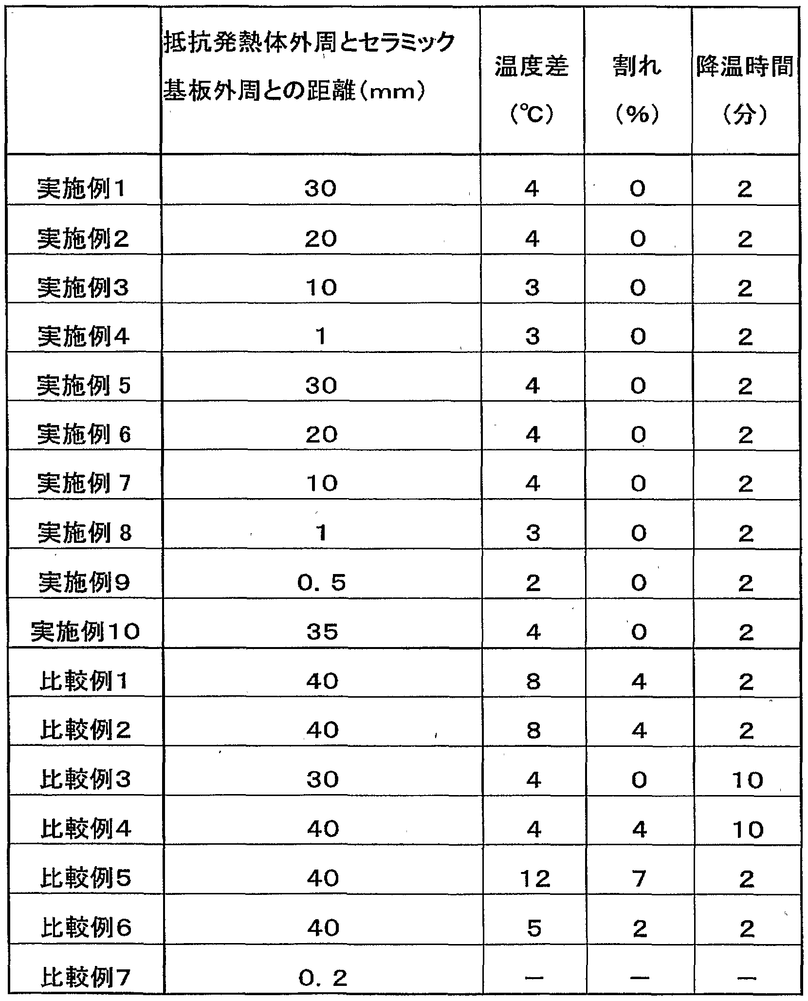
- the heaters of the example and the comparative example were assembled into a support container as shown in Fig. 3 to form a unit, and the temperature was raised to 400 ° C. -16-2012-0012). Further, the temperature was raised to 400 ° C. in 45 seconds, and the incidence of cracking was examined. In addition, from 200 ° C to 150 Table 1 shows the results of measuring the cooling time by blowing air to ° C and forcibly cooling.
- the cooling time can be shortened by forming the resistance heating element on the surface.
- the temperature difference on the heated surface is increased (compared to Comparative Example 24).
- the resistance heating element by forming below 3 5 mm from Ceramic substrate side, the temperature difference between the heating surface is reduced t In addition, it does not crack even when the temperature is rapidly increased (Examples 1 to 10 are compared with Comparative Examples). Also, from a comparison between Comparative Example 1 and Comparative Example 5, it can be seen that the temperature difference increases as the diameter of the ceramic substrate increases.
- the present invention solves the problem of lowering the outer peripheral temperature caused by a large ceramic heater having a diameter exceeding 15 Omm, and the effect is remarkable when the diameter exceeds 21 Omm. Possibility of industrial use
Landscapes
- Chemical & Material Sciences (AREA)
- Engineering & Computer Science (AREA)
- Ceramic Engineering (AREA)
- Surface Heating Bodies (AREA)
- Resistance Heating (AREA)
Description
Claims
Priority Applications (1)
| Application Number | Priority Date | Filing Date | Title |
|---|---|---|---|
| EP01926084A EP1231820A1 (en) | 2000-05-02 | 2001-05-01 | Ceramic heater |
Applications Claiming Priority (2)
| Application Number | Priority Date | Filing Date | Title |
|---|---|---|---|
| JP2000-133942 | 2000-05-02 | ||
| JP2000133942 | 2000-05-02 |
Publications (1)
| Publication Number | Publication Date |
|---|---|
| WO2001084885A1 true WO2001084885A1 (en) | 2001-11-08 |
Family
ID=18642322
Family Applications (1)
| Application Number | Title | Priority Date | Filing Date |
|---|---|---|---|
| PCT/JP2001/003759 Ceased WO2001084885A1 (en) | 2000-05-02 | 2001-05-01 | Ceramic heater |
Country Status (3)
| Country | Link |
|---|---|
| US (1) | US20020155262A1 (ja) |
| EP (1) | EP1231820A1 (ja) |
| WO (1) | WO2001084885A1 (ja) |
Families Citing this family (11)
| Publication number | Priority date | Publication date | Assignee | Title |
|---|---|---|---|---|
| EP1249433A4 (en) * | 1999-09-06 | 2005-01-05 | Ibiden Co Ltd | BRICKET AND CERAMIC SUBSTRATE OF SINKED CARBON CONTAINING ALUMINUM NITRIDE FOR USE IN DEVICES FOR MANUFACTURING AND STUDYING SEMICONDUCTORS |
| US6861165B2 (en) * | 2000-02-24 | 2005-03-01 | Ibiden Co., Ltd. | Aluminum nitride sintered compact, ceramic substrate, ceramic heater and electrostatic chuck |
| JP2001247382A (ja) * | 2000-03-06 | 2001-09-11 | Ibiden Co Ltd | セラミック基板 |
| EP1233651A1 (en) * | 2000-04-07 | 2002-08-21 | Ibiden Co., Ltd. | Ceramic heater |
| JP3516392B2 (ja) * | 2000-06-16 | 2004-04-05 | イビデン株式会社 | 半導体製造・検査装置用ホットプレート |
| EP1229572A1 (en) * | 2000-07-04 | 2002-08-07 | Ibiden Co., Ltd. | Hot plate for semiconductor manufacture and testing |
| US6815646B2 (en) * | 2000-07-25 | 2004-11-09 | Ibiden Co., Ltd. | Ceramic substrate for semiconductor manufacture/inspection apparatus, ceramic heater, electrostatic clampless holder, and substrate for wafer prober |
| US20060088692A1 (en) * | 2004-10-22 | 2006-04-27 | Ibiden Co., Ltd. | Ceramic plate for a semiconductor producing/examining device |
| US8294069B2 (en) * | 2007-03-28 | 2012-10-23 | Ngk Insulators, Ltd. | Heating device for heating a wafer |
| US8252410B2 (en) * | 2007-09-05 | 2012-08-28 | Applied Materials, Inc. | Ceramic cover wafers of aluminum nitride or beryllium oxide |
| JP5834905B2 (ja) * | 2011-12-27 | 2015-12-24 | 富士通株式会社 | 加熱装置及び加熱方法 |
Citations (2)
| Publication number | Priority date | Publication date | Assignee | Title |
|---|---|---|---|---|
| JPH04119990U (ja) * | 1991-04-09 | 1992-10-27 | 信越化学工業株式会社 | ウエ−ハ状積層セラミツクスヒ−タ− |
| JPH1140330A (ja) * | 1997-07-19 | 1999-02-12 | Ibiden Co Ltd | ヒーターおよびその製造方法 |
Family Cites Families (7)
| Publication number | Priority date | Publication date | Assignee | Title |
|---|---|---|---|---|
| US240648A (en) * | 1881-04-26 | Charles bltjst | ||
| US247451A (en) * | 1881-09-20 | Territory | ||
| US238955A (en) * | 1881-03-15 | sweet | ||
| US246590A (en) * | 1881-09-06 | Elmee e | ||
| US247551A (en) * | 1881-09-27 | Patrick fitzgibbons | ||
| US246909A (en) * | 1881-09-13 | Apparatus for operating fans | ||
| US248168A (en) * | 1881-10-11 | harvey |
-
2001
- 2001-05-01 WO PCT/JP2001/003759 patent/WO2001084885A1/ja not_active Ceased
- 2001-05-01 EP EP01926084A patent/EP1231820A1/en not_active Withdrawn
- 2001-05-01 US US10/019,448 patent/US20020155262A1/en not_active Abandoned
Patent Citations (2)
| Publication number | Priority date | Publication date | Assignee | Title |
|---|---|---|---|---|
| JPH04119990U (ja) * | 1991-04-09 | 1992-10-27 | 信越化学工業株式会社 | ウエ−ハ状積層セラミツクスヒ−タ− |
| JPH1140330A (ja) * | 1997-07-19 | 1999-02-12 | Ibiden Co Ltd | ヒーターおよびその製造方法 |
Also Published As
| Publication number | Publication date |
|---|---|
| EP1231820A1 (en) | 2002-08-14 |
| US20020155262A1 (en) | 2002-10-24 |
Similar Documents
| Publication | Publication Date | Title |
|---|---|---|
| US6677557B2 (en) | Ceramic heater | |
| WO2001013679A1 (en) | Ceramic heater | |
| WO2003007661A1 (en) | Ceramic heater and ceramic joined article | |
| WO2001041508A1 (en) | Ceramic heater | |
| WO2001011923A1 (en) | Ceramic heater | |
| WO2002003434A1 (fr) | Radiateur ceramique pour appareil de fabrication ou de test de semi-conducteurs | |
| WO2001078456A1 (fr) | Element ceramique chauffant | |
| JP3729785B2 (ja) | セラミックヒータ | |
| WO2001011922A1 (en) | Ceramic heater | |
| WO2001080307A1 (en) | Ceramic substrate | |
| WO2001078455A1 (fr) | Plaque ceramique | |
| WO2002045138A1 (fr) | Dispositif ceramique chauffant permettant la production de semi-conducteurs et dispositifs d'inspection | |
| JPWO2001080601A1 (ja) | セラミックヒータ | |
| WO2001084885A1 (en) | Ceramic heater | |
| JP2001230059A (ja) | 半導体製造・検査装置用セラミック基板 | |
| JP3625046B2 (ja) | 半導体製造・検査装置用セラミックヒータ | |
| JP2001332560A (ja) | 半導体製造・検査装置 | |
| JP2004303736A (ja) | セラミックヒータ | |
| JP2002141257A (ja) | 半導体製造・検査装置用セラミックヒータ | |
| JP2002334820A (ja) | 半導体ウエハまたは液晶基板加熱用セラミックヒータ | |
| JP2002319525A (ja) | 半導体製造・検査装置用セラミックヒータ | |
| JP2002305073A (ja) | セラミックヒータ | |
| JP2002100462A (ja) | ホットプレート | |
| JP2001130982A (ja) | 半導体製造装置用セラミック板 | |
| JP2001358205A (ja) | 半導体製造・検査装置 |
Legal Events
| Date | Code | Title | Description |
|---|---|---|---|
| AK | Designated states |
Kind code of ref document: A1 Designated state(s): JP US |
|
| AL | Designated countries for regional patents |
Kind code of ref document: A1 Designated state(s): AT BE CH CY DE DK ES FI FR GB GR IE IT LU MC NL PT SE TR |
|
| ENP | Entry into the national phase |
Ref country code: JP Ref document number: 2001 581576 Kind code of ref document: A Format of ref document f/p: F |
|
| 121 | Ep: the epo has been informed by wipo that ep was designated in this application | ||
| WWE | Wipo information: entry into national phase |
Ref document number: 2001926084 Country of ref document: EP |
|
| WWE | Wipo information: entry into national phase |
Ref document number: 10019448 Country of ref document: US |
|
| WWP | Wipo information: published in national office |
Ref document number: 2001926084 Country of ref document: EP |
|
| WWW | Wipo information: withdrawn in national office |
Ref document number: 2001926084 Country of ref document: EP |