WO2002065722A1 - Digital modulation system, radio communication system, radio communication device - Google Patents
Digital modulation system, radio communication system, radio communication device Download PDFInfo
- Publication number
- WO2002065722A1 WO2002065722A1 PCT/JP2001/000955 JP0100955W WO02065722A1 WO 2002065722 A1 WO2002065722 A1 WO 2002065722A1 JP 0100955 W JP0100955 W JP 0100955W WO 02065722 A1 WO02065722 A1 WO 02065722A1
- Authority
- WO
- WIPO (PCT)
- Prior art keywords
- data
- transmission
- digital
- dummy data
- wireless communication
- Prior art date
- Legal status (The legal status is an assumption and is not a legal conclusion. Google has not performed a legal analysis and makes no representation as to the accuracy of the status listed.)
- Ceased
Links
Classifications
-
- H—ELECTRICITY
- H04—ELECTRIC COMMUNICATION TECHNIQUE
- H04L—TRANSMISSION OF DIGITAL INFORMATION, e.g. TELEGRAPHIC COMMUNICATION
- H04L27/00—Modulated-carrier systems
- H04L27/18—Phase-modulated carrier systems, i.e. using phase-shift keying
-
- H—ELECTRICITY
- H04—ELECTRIC COMMUNICATION TECHNIQUE
- H04L—TRANSMISSION OF DIGITAL INFORMATION, e.g. TELEGRAPHIC COMMUNICATION
- H04L7/00—Arrangements for synchronising receiver with transmitter
- H04L7/04—Speed or phase control by synchronisation signals
- H04L7/041—Speed or phase control by synchronisation signals using special codes as synchronising signal
- H04L2007/045—Fill bit or bits, idle words
Definitions
- the present invention relates to a digital modulation method for inserting a dummy data into digital data to be transmitted so that a digital data transmitted from a transmission side can be accurately demodulated on a reception side, and a wireless communication system to which the digital modulation method is applied.
- the method relates to a wireless communication device.
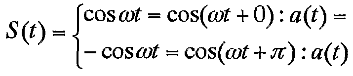
- a PSK (Pose Shift Keying) method in which the phase of a carrier wave is discretely changed according to the digital data to be transmitted (hereinafter referred to as transmission data).
- the simplest is the BPSK (Binar Phase Shift Keying) modulation method.
- This BPSK modulation method is a binary transmission method that changes the phase of the carrier c 0 s ⁇ t to 0, ⁇ ⁇ , corresponding to the transmission data 0,1.
- the BPSK modulated wave S (t) is represented by the following equation.
- transmit data carrier BPSK modulated wave, band-limited BPS
- FIG. 1 shows the relationship between the K modulated waves.
- the BPSK modulated wave S (t) is generated by the following method. In FIG. 2, first, the level is set to +1, 11 for transmission data a (t) 0 (for transmission data 0) and 1 (for transmission data 1). The conversion unit 1 performs level conversion. Then, the BPSK signal S (t) is obtained by multiplying the transmission data a (t) subjected to the level conversion by the carrier cos ⁇ t by the multiplier 2 and passing through the BPF (B and Pass F i 1 ter) 3. It is.
- This processing is represented by an equation as follows. From this equation, it can be seen that the phase modulation of 0, has been achieved by multiplying the level-converted transmission data a (t) by the carrier cos ⁇ t. +1
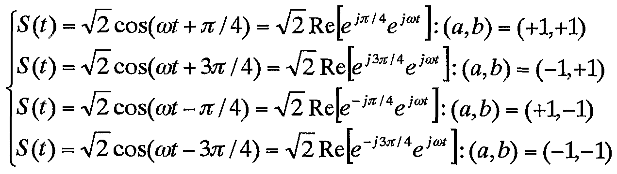
- the QPSK modulation method is a quaternary transmission PSK method in which information is transmitted two bits at a time for each symbol time by taking four types of phases.
- the phase of the carrier cos ⁇ t is set to 4 in accordance with the 2-bit transmission data (0, 0), (1, 0), (1, 1), (0, 1).
- 34 in the case of transmission data (1, 0)
- 13/4 in the case of transmission data (1, 1, 1)
- — ⁇ Change to / 4 in the case of transmission data (0, 1)
- the QPSK modulated wave S (t) is represented by the following equation.
- the transmission data is serial-to-parallel converted into two sequences a (t) and b (t) by the serial-to-parallel converter 4 as shown in FIG. — Evening 0, 1 is converted to +1, -1, so that a (t) and b (t) signals are created.
- E jwt in R e [] represents the oscillation of the carrier wave, and the information is on e ⁇ Z 4 , e j 3? R / 4 , e ⁇ i 7C / 4 , and e- j 37r / 4 . As is clear from this, we take four phases.
- the phase mapping signals of Ich and Qch indicate transmission OFF. Will be taken.
- the phase moving signal takes three values (1, 0, -1) and takes eight values on the I / Q plane. Therefore, on the receiving side, when trying to demodulate the data that takes 8 values, when comparing the positive / negative of the phase matching signal of [10] and 011, the decision threshold for the reception decision is made.
- the data is mapped on the field line and demodulation is not performed normally at the time of demodulation, and the demodulation performance is deteriorated.
- the present invention has been made to solve the conventional problems as described above.
- a demodulation performance when transmission is set to 0FF in bit units with respect to transmission data. It is an object of the present invention to provide a digital modulation system capable of reducing deterioration of a radio communication system, a radio communication system to which the digital modulation system is applied, and a radio communication device. Disclosure of the invention
- a phase mapping signal pair converted into a phase mapping signal pair of Ich and Qch based on an I / Q plane predetermined by a QPSK modulation method is bit-wise.
- dummy data is inserted in all the transmission FF portions in accordance with the transmission FF evening.
- the phase matching signal pair of Ich and Qch which has taken eight values on the I / Q plane, takes four values, and when comparing the positive / negative of the phase matching of Ich and Qch.
- the digital modulation method according to the present invention is determined in advance by the QPSK modulation method. Based on the obtained I / Q plane, it is converted into a pair of phase mapping signals of Ich and Qch, and the obtained pair of phase matching signals is transmitted in units of bits. When 0FF continues and only one of the phase matching signal pair is transmission 0FF, dummy data is inserted in the transmission 0FF portion in accordance with the evening of transmission 0FF.
- the phase pine of Ich and Qch which had taken 8 values on the I / Q plane, now has a 4-valued pair of Bing signals, and the phase pine of Ich and Qch has positive and negative
- the effect that it is possible to prevent the overnight mapping on the judgment boundary line for the reception judgment, to reduce the deterioration of the demodulation performance at the time of demodulation, and to suppress the transmission power. is there.
- a wireless communication system modulates digital data to be transmitted by a digital modulation method that inputs dummy data in accordance with the timing of transmission 0 FF, and transmits the modulated digital data.
- a wireless communication apparatus includes a digital modulator that employs a digital modulation method in which dummy data is inserted into digital data to be transmitted in accordance with a transmission time of 0 FF.
- a wireless communication apparatus includes: a dummy data generator that inserts dummy data in synchronization with transmission of digital data to be transmitted at a timing of 0FF; and a digital data generator that transmits the dummy data with the dummy data inserted. It comprises a level converter for performing level conversion, and a digital modulator having a multiplier for multiplying the output of the level converter by a carrier. This has the effect of reducing the degradation of demodulation performance during demodulation on the receiving side.
- a wireless communication apparatus includes a serial-parallel conversion unit that converts digital data to be transmitted into two series, and inserts a dummy data in accordance with the timing of transmission OFF of the digital data converted into the two series.
- a dummy data generator that performs the level conversion of the transmission digital data input into which the dummy data is input, and a phase converter that converts the two sets of transmission digital data output from the level converter. Is provided with a digital modulator having a multiplier for multiplying carriers different by 180 degrees.
- the digital modulation method according to the present invention is a digital modulation method in wireless communication, wherein a symbol denoting DTX (Disconti nu ous T ran sm ission) in a CDMA (Code Division Multiple Access 1 e Access method) is performed.
- DTX Disconti nu ous T ran sm ission
- CDMA Code Division Multiple Access 1 e Access method
- phase matching signals of Ich and Qch are symbol data indicating DTX
- dummy data is inserted in all portions of symbol data indicating DTX. It is modulated by the digital modulation method and transmitted.
- the wireless communication apparatus when the phase matching signals of I ch and Q ch are symbol data indicating DTX, dummy data is input to all parts of symbol data indicating DTX. It is equipped with a digital modulator that adopts a digital modulation system that performs the following.
- the digital modulation scheme according to the present invention is a CDMA (Code Division Multiple Access) scheme, which is used to insert symbol data indicating D TX (Disconti nu ous Tran sm ission) into a downlink physical channel.
- D TX Disconti nu ous Tran sm ission
- a dummy data is inserted into the symbol data indicating the DTX.
- the wireless communication method according to the present invention is a digital modulation method that inserts dummy data into a portion of the symbol data indicating DTX when one of the phase matching signals of Ich and Qch is symbol data indicating DTX. It adopts the system.
- one of the phase matching signals of the I ch and the Q ch is! If the symbol data indicates TX, a digital modulator adopting a digital modulation method that inserts dummy data into the portion of the symbol data indicating DTX is provided. As a result, it is possible to reduce the degradation of demodulation performance during demodulation and to suppress the transmission power, which can be realized without increasing interference.
- Fig. 1 shows transmitted data, carrier, BPSK modulated wave, band-limited BP
- FIG. 6 is a waveform chart showing a relationship between SK modulated waves.
- FIG. 2 is a circuit diagram for generating a BPSK modulated wave.
- FIG. 3 is a circuit diagram for generating a QPSK modulated wave.
- FIG. 4 is a diagram showing the relationship between transmission data and data after serial-parallel conversion.
- FIG. 5 is a configuration diagram of a BPSK modulator according to the first embodiment.
- FIG. 6 is an explanatory diagram of a method for inserting data.
- FIG. 7 is a configuration diagram of a BPSK demodulator according to the present invention.
- FIG. 8 is a relationship diagram between transmission data and dummy position information.
- FIG. 9 is a first explanatory diagram of a dummy data insertion method during QPSK modulation.
- FIG. 10 is a second explanatory diagram of a dummy data insertion method at the time of QPSK modulation.
- FIG. 11 is a block diagram of a QPSK modulator according to the present invention.
- FIG. 12 is a block diagram of the QPSK demodulator according to the present invention.
- FIG. 13 is a signal space diagram of the QPSK modulated signal.
- FIG. 14 is a mapping diagram at the time of transmission 0 FF.
- FIG. 15 is a transmission data diagram including DTX information.
- FIG. 16 is a first explanatory diagram of a method of inserting a dummy data into the transmission FF position.
- FIG. 17 is a second explanatory diagram of a method of inserting a dummy data into the transmission FF position.
- FIG. 5 is a configuration diagram of a BPSK modulator according to the present invention
- FIG. 6 is an explanatory diagram of a dummy data insertion method
- FIG. 7 is a configuration diagram of a BPSK demodulator.
- 11 is a level converter, which converts the signal of the transmission data (0, 1) into (+1, -1).
- 1 2 is a dummy data generator
- 13 is a BPF
- 14 is an adder that adds dummy data to the transmission data at the timing of transmission 0FF
- 15 is a level-converted transmission data and carrier cos ⁇ t , And is transmitted as a modulated wave S (t) through the multiplier 15 and the BPF 13.
- the method of inserting dummy data will be described with reference to FIG. Insert the dummy data generated by the dummy data generator 1 and 2 according to the timing of transmission 0 F F included in the transmission data. After that, the data sequence in which the dummy data is inserted is level-converted by the level converter 11 and transmitted through modulation processing.
- the transmitted BPSK modulated wave is multiplied by the reference carrier cos ⁇ t by the multiplier 21 and then passed through the LPF (Low Pass Filter) 22.
- LPF Low Pass Filter
- the discriminating unit 23 to make a hard decision.
- the data output from the identification unit 23 is subjected to level conversion (0, 1) by the level converter 24, and from the information sent from the dummy data position information generator 25, which evening signal is dummy data
- the signal discriminator 26 if the data is dummy data, it is replaced with a signal indicating transmission OFF and restored.
- transmission OFF timing Since it is possible to delete the dummy data inserted in the demodulator, it is possible to reduce the deterioration of the demodulation performance at the time of demodulation due to transmission 0FF.
- the transmission data (transmission bit sequence) has a time zone in which no data is transmitted with respect to the time axis (dotted line in Fig. 8). Therefore, if the data is received on the receiving side, the demodulation performance will be degraded. Therefore, the time period during which data is actually transmitted is represented by 1 as dummy data position information, and the time period during which data is not transmitted is represented by 0. In addition, if there is a delay in a time period during which transmission is not being performed, the deterioration of demodulation performance can be reduced. Therefore, a delay is transmitted at a timing when transmission is not being performed. The value of the dummy data to be inserted is 0 or 1.
- the transmission data sequence including the transmission OFF symbol is separated into Ich and Qch phase matching signals, and the transmission data sequence is synchronized with all transmission 0FFs included in the transmitted data. Dummy data generated by one data generator is inserted for processing.
- the phase matching signal pair of Ich and Qch which has taken eight values on the I / Q plane, takes four values, and the Ich and Qch
- the Ich and Qch When comparing the positive / negative of the phase mapping, it is possible to prevent the data from being mapped on the determination boundary line for the reception determination and to reduce the deterioration of the demodulation performance at the time of demodulation.
- the transmission data sequence including the transmission FF symbol is separated into the Ich and Qch phase matching signals, and among the transmitted data, the Ich and Qch signal pairs are considered. If only one of them contains a transmission FF symbol, a dummy data is inserted at the transmission FF timing. By doing so, compared to a case where dummy data is inserted into all transmission OFF symbol sections, transmission of unnecessary dummy data is not performed and transmission power can be suppressed.
- the phase matching signal pair of Ich and Qch which has taken eight values on the I / Q plane, takes four values, and the Ich and Qch
- FIG. 11 shows a configuration diagram of a QPSK modulator according to Embodiment 4 of the present invention.
- a transmission data is input to a serial / parallel converter 18 and is subjected to parallel conversion to form two columns. It is output as a parallel data series. After that, the two columns of parallel data sequence are added with the dummy data from the dummy data generator 12 in all parts indicating transmission FF in accordance with the timing of transmission FF. , 17 b and then input to the level converter 11.
- the level converter 11 inputs a two-column parallel data sequence (0, 1), converts the data level into (+1, -1), and outputs the result.
- Multipliers 18 a and 18 b provide carrier waves in two columns of output data After multiplying by cos ⁇ tssin ⁇ t and adding by an adder 19, the signal passes through the BPF 13 and is transmitted as a QPSK modulated signal.
- '' Fig. 12 is a diagram showing the configuration of the QPSK demodulator according to the present invention.In the transmitted QPSK modulation data, the reference carrier 2 c 0 s ⁇ t After multiplying the reference carrier 2 si ⁇ t by 27 b, the signal is passed through LPFs 28 a and 28 b and input to the discriminator 23, where hard decision is performed.
- the ⁇ 1 data output from the identification unit 23 is level-converted by the level converter 24, and the timing signal from the information sent from the dummy data position information generator 25 is dummy data.
- the signal judging sections 29 a and 29 b determine whether the signal is dummy data and replace the signal at the location determined to be dummy data with data representing transmission 0 FF, input to the parallel-serial converter 30, and demodulate data as Is output. This can reduce performance degradation during demodulation.
- FIG. 13 shows a signal space diagram of the QPSK modulation signal.
- demodulation is performed using the data in which the dummy data has been inserted. After demodulation, if data indicating transmission 0 FF is inserted in bits at a point indicating transmission 0 FF based on the dummy data insertion position information, the same data as that input on the transmission side is obtained. An overnight sequence can be obtained, and the deterioration of demodulation performance can be reduced.
- the signal mapped to the origin is determined as a signal of transmission 0 FF and demodulated, so that the restored data is transmitted with the transmission data input on the transmission side.
- the demodulation performance can be reduced.
- the downlink two consecutive symbol pairs are subjected to serial / parallel conversion, and separated into Ich and Qch signals.
- the Ich and Qch signals thus divided include DTX indicating transmission 0FF. Therefore, the degradation of demodulation performance is reduced by replacing the bit data of DTX indicating transmission 0FF with the dummy data.
- information indicating whether the data transmission is the original data transmission or the dummy data transmission is also transmitted at the same time.
- the transmission part of the dummy data is transmitted based on the position information of the dummy data.
- the original data can be restored, and the deterioration of the demodulation performance can be reduced. In other words, it does not transmit only the Ich and Qch signals generated when the transmission data is parallel-converted, but indicates the transmission OFF for each data sequence.
- a data sequence including the TX information is also transmitted at the same time.
- the transmission 0 FF is also included in the data transmission of Q ch. Therefore, the dummy data is inserted into each of I ch and Q ch in accordance with the timing of transmission 0 F F as described above. At that time, DTX information data is created by inserting 1 for the actual data portion and 0 for the dummy data portion as dummy data insertion position information for each of I ch and Q ch. At the same time as transmitting the data of I ch and Q ch, the DTX information data is also transmitted.
- the receiving side receives the transmitted data and the data indicating the insertion position information of the dummy data, and demodulates the transmitted data. Then, the restored data is compared with the data indicating the insertion position information of the dummy data, and the data of the dummy data insertion portion indicated by the dummy data insertion position information is transmitted with respect to the restored data. By exchanging the information, it is possible to reduce performance degradation at the time of demodulation due to transmission 0FF.
- the dummy data generator 25 described above indicates transmission 0FF by inserting before the level conversion of the transmission data on the transmission side.
- the above-described processing can be performed by performing the modulation by replacing the symbols with the dummy data.
- the dummy data insertion position information is inserted after the process of performing level conversion at the time of demodulating the received data, so that a symbol of transmission 0 FF can be inserted into the reception data overnight. This means that the same data as that input to the transmitter is restored.
- Embodiment 5 it is possible to reduce deterioration of demodulation performance at the time of demodulation on the receiving side.
- the dummy data generator 12 and the dummy data insertion position information generator 25 described above are mounted on a base station and a terminal adopting the CDMA system, and are used for a wireless communication system. Performance degradation can be reduced.
- Embodiment 6
- a pair of signal pairs is a sequence of I ch and Q ch data when the transmission data is parallel-converted.
- the Ich and Qch signals transmitted in the same time zone are called a signal pair.
- the adjacent data is called a pair signal.
- the pair of signal pairs in Fig. 17 is the one with the same number below I and Q.
- both of the paired signal pairs are transmission FFs, the data is not replaced with the dummy data, and the information of the transmission FF is not replaced. To send the insertion position information. This makes it possible to reduce the degradation in performance during demodulation by inserting dummy data only in the part necessary for demodulation as an Ich ZQch signal pair and demodulating.
- the receiving side receives the transmitted data and the data indicating the insertion position information of the dummy data and demodulates the transmitted data. Thereafter, the restored data is compared with the data indicating the insertion position information of the dummy data, and the data of the dummy data insertion portion indicated by the dummy data insertion position information is transmitted with respect to the restored data.
- the dummy data generator 12 inserts a symbol indicating transmission FF into dummy data on the transmitting side before performing a process of performing level conversion of transmission data, and performs modulation by performing the modulation.
- the processing described above becomes possible.
- the dummy data position information generator 25 can insert the symbol of transmission OFF over the reception data by inserting it after performing the level conversion processing when demodulating the received data. Then, the same data as the data input to the transmitting side is restored.
- Embodiment 6 at the time of demodulation on the receiving side, degradation of demodulation performance can be reduced.
- the dummy data generator 12 and the dummy data insertion position information generator 25 are mounted on a base station and a terminal adopting the CDMA system and used for a wireless communication system, so that the demodulation performance by transmission FF is achieved. Degradation can be reduced. Industrial applicability
- the digital modulation scheme in the wireless communication according to the present invention is This is effective for reducing the deterioration of the demodulation performance on the receiving side.
Landscapes
- Engineering & Computer Science (AREA)
- Computer Networks & Wireless Communication (AREA)
- Signal Processing (AREA)
- Digital Transmission Methods That Use Modulated Carrier Waves (AREA)
Description
Claims
Priority Applications (5)
| Application Number | Priority Date | Filing Date | Title |
|---|---|---|---|
| US10/240,272 US20030108122A1 (en) | 2001-02-09 | 2001-02-09 | Digital modulation system, radio communication system, radio communication device |
| EP01902838A EP1267534A4 (en) | 2001-02-09 | 2001-02-09 | DIGITAL MODULATION PROCESS, RADIO SWITCHING SYSTEM, RADIO SWITCHING DEVICE |
| JP2002564910A JPWO2002065722A1 (ja) | 2001-02-09 | 2001-02-09 | デジタル変調方式、無線通信方式、無線通信装置 |
| CN01807839.7A CN1422478A (zh) | 2001-02-09 | 2001-02-09 | 数字调制方式,无线通信方式,无线通信装置 |
| PCT/JP2001/000955 WO2002065722A1 (en) | 2001-02-09 | 2001-02-09 | Digital modulation system, radio communication system, radio communication device |
Applications Claiming Priority (1)
| Application Number | Priority Date | Filing Date | Title |
|---|---|---|---|
| PCT/JP2001/000955 WO2002065722A1 (en) | 2001-02-09 | 2001-02-09 | Digital modulation system, radio communication system, radio communication device |
Publications (1)
| Publication Number | Publication Date |
|---|---|
| WO2002065722A1 true WO2002065722A1 (en) | 2002-08-22 |
Family
ID=11737009
Family Applications (1)
| Application Number | Title | Priority Date | Filing Date |
|---|---|---|---|
| PCT/JP2001/000955 Ceased WO2002065722A1 (en) | 2001-02-09 | 2001-02-09 | Digital modulation system, radio communication system, radio communication device |
Country Status (5)
| Country | Link |
|---|---|
| US (1) | US20030108122A1 (ja) |
| EP (1) | EP1267534A4 (ja) |
| JP (1) | JPWO2002065722A1 (ja) |
| CN (1) | CN1422478A (ja) |
| WO (1) | WO2002065722A1 (ja) |
Cited By (2)
| Publication number | Priority date | Publication date | Assignee | Title |
|---|---|---|---|---|
| JP2019012983A (ja) * | 2017-07-03 | 2019-01-24 | 株式会社日立製作所 | 受信機、送信機、および無線通信機 |
| JP2023110054A (ja) * | 2015-06-17 | 2023-08-08 | パナソニック インテレクチュアル プロパティ コーポレーション オブ アメリカ | 送信方法、受信方法、送信装置、及び受信装置 |
Families Citing this family (3)
| Publication number | Priority date | Publication date | Assignee | Title |
|---|---|---|---|---|
| EP3402147B1 (en) | 2005-08-05 | 2020-09-30 | Panasonic Corporation | Radio communication apparatus and radio communication method for modulation symbol mapping |
| IN2011KN02769A (ja) * | 2009-02-09 | 2015-07-10 | Huawei Tech Co Ltd | |
| CN103532670A (zh) * | 2013-10-13 | 2014-01-22 | 西安电子科技大学 | 数字通信中的压缩调制和实时解调方法 |
Citations (9)
| Publication number | Priority date | Publication date | Assignee | Title |
|---|---|---|---|---|
| JPS62176243A (ja) * | 1986-01-30 | 1987-08-03 | Nec Corp | Tdma用fsk変調器安定化方法 |
| JPH0583208A (ja) * | 1991-05-31 | 1993-04-02 | Kokusai Electric Co Ltd | 音声符号化通信方式及びその装置 |
| JPH08500475A (ja) * | 1993-06-14 | 1996-01-16 | テレフオンアクチーボラゲツト エル エム エリクソン | Ds−cdmaシステムにおけるシームレス・ハンドオーバーのための不連続送信 |
| JPH08501665A (ja) * | 1992-04-10 | 1996-02-20 | エリクソン ジーイー モービル コミュニケーションズ インコーポレイテッド | 不連続cdma受信方式 |
| JPH09102759A (ja) * | 1995-10-06 | 1997-04-15 | Hitachi Denshi Ltd | 送信機 |
| JPH09261172A (ja) * | 1996-03-22 | 1997-10-03 | Matsushita Electric Ind Co Ltd | 移動通信装置 |
| JPH10513318A (ja) * | 1995-01-31 | 1998-12-15 | ノキア モービル フォーンズ リミテッド | 移動電話システムにおいて不連続送信を実現する方法 |
| JPH1174835A (ja) * | 1997-06-26 | 1999-03-16 | Nokia Mobile Phones Ltd | 移動局を動作させるための方法及び符号分割多元接続(cdma)移動局を動作させるための方法及び無線データ端末 |
| JP2000101476A (ja) * | 1998-09-22 | 2000-04-07 | Canon Inc | 無線通信装置、無線通信システム及び無線通信方法 |
Family Cites Families (5)
| Publication number | Priority date | Publication date | Assignee | Title |
|---|---|---|---|---|
| JPH0472939A (ja) * | 1990-07-13 | 1992-03-06 | Hitachi Ltd | 光スイッチを用いたパケット交換装置 |
| AU659189B2 (en) * | 1991-05-29 | 1995-05-11 | Comsat Corporation | Fully meshed CDMA network for personal communications terminals |
| FI100211B (fi) * | 1995-03-06 | 1997-10-15 | Nokia Telecommunications Oy | Suurinopeuksinen datasiirto matkaviestinverkoissa |
| FR2799320B1 (fr) * | 1999-10-04 | 2002-05-17 | Mitsubishi Electric France | Procede d'equilibrage de debit entre des canaux de transport de donnees, dispositif, station de base et station mobile correspondants |
| US6934317B1 (en) * | 2000-10-11 | 2005-08-23 | Ericsson Inc. | Systems and methods for communicating spread spectrum signals using variable signal constellations |
-
2001
- 2001-02-09 CN CN01807839.7A patent/CN1422478A/zh active Pending
- 2001-02-09 WO PCT/JP2001/000955 patent/WO2002065722A1/ja not_active Ceased
- 2001-02-09 US US10/240,272 patent/US20030108122A1/en not_active Abandoned
- 2001-02-09 EP EP01902838A patent/EP1267534A4/en not_active Withdrawn
- 2001-02-09 JP JP2002564910A patent/JPWO2002065722A1/ja active Pending
Patent Citations (9)
| Publication number | Priority date | Publication date | Assignee | Title |
|---|---|---|---|---|
| JPS62176243A (ja) * | 1986-01-30 | 1987-08-03 | Nec Corp | Tdma用fsk変調器安定化方法 |
| JPH0583208A (ja) * | 1991-05-31 | 1993-04-02 | Kokusai Electric Co Ltd | 音声符号化通信方式及びその装置 |
| JPH08501665A (ja) * | 1992-04-10 | 1996-02-20 | エリクソン ジーイー モービル コミュニケーションズ インコーポレイテッド | 不連続cdma受信方式 |
| JPH08500475A (ja) * | 1993-06-14 | 1996-01-16 | テレフオンアクチーボラゲツト エル エム エリクソン | Ds−cdmaシステムにおけるシームレス・ハンドオーバーのための不連続送信 |
| JPH10513318A (ja) * | 1995-01-31 | 1998-12-15 | ノキア モービル フォーンズ リミテッド | 移動電話システムにおいて不連続送信を実現する方法 |
| JPH09102759A (ja) * | 1995-10-06 | 1997-04-15 | Hitachi Denshi Ltd | 送信機 |
| JPH09261172A (ja) * | 1996-03-22 | 1997-10-03 | Matsushita Electric Ind Co Ltd | 移動通信装置 |
| JPH1174835A (ja) * | 1997-06-26 | 1999-03-16 | Nokia Mobile Phones Ltd | 移動局を動作させるための方法及び符号分割多元接続(cdma)移動局を動作させるための方法及び無線データ端末 |
| JP2000101476A (ja) * | 1998-09-22 | 2000-04-07 | Canon Inc | 無線通信装置、無線通信システム及び無線通信方法 |
Non-Patent Citations (1)
| Title |
|---|
| See also references of EP1267534A4 * |
Cited By (4)
| Publication number | Priority date | Publication date | Assignee | Title |
|---|---|---|---|---|
| JP2023110054A (ja) * | 2015-06-17 | 2023-08-08 | パナソニック インテレクチュアル プロパティ コーポレーション オブ アメリカ | 送信方法、受信方法、送信装置、及び受信装置 |
| JP7526315B2 (ja) | 2015-06-17 | 2024-07-31 | パナソニック インテレクチュアル プロパティ コーポレーション オブ アメリカ | 送信方法、受信方法、送信装置、及び受信装置 |
| JP2019012983A (ja) * | 2017-07-03 | 2019-01-24 | 株式会社日立製作所 | 受信機、送信機、および無線通信機 |
| JP7000051B2 (ja) | 2017-07-03 | 2022-01-19 | 株式会社日立製作所 | 受信機、送信機、および無線通信機 |
Also Published As
| Publication number | Publication date |
|---|---|
| US20030108122A1 (en) | 2003-06-12 |
| EP1267534A4 (en) | 2003-06-18 |
| CN1422478A (zh) | 2003-06-04 |
| EP1267534A1 (en) | 2002-12-18 |
| JPWO2002065722A1 (ja) | 2004-06-17 |
Similar Documents
| Publication | Publication Date | Title |
|---|---|---|
| US8369425B2 (en) | Robust channel estimation in communication systems | |
| US8189453B2 (en) | Method of OFDM communication using superposition coding | |
| EP0949765A2 (en) | Digital modulation system using extended code set | |
| EP2262160B1 (en) | Apparatus and method for digital wireless communications | |
| CN101267412A (zh) | 发射机和接收机 | |
| US6363100B1 (en) | Radio data communication system using spread spectrum scheme | |
| JPH10308717A (ja) | 受信装置および受信方法 | |
| WO2001013559A1 (fr) | Emetteur de signaux multiporteuses et recepteur de signaux multiporteuses | |
| WO2002065722A1 (en) | Digital modulation system, radio communication system, radio communication device | |
| JP6292755B2 (ja) | 送信機、受信機および送信方法 | |
| CN101189846B (zh) | 用于检测数据符号的方法和接收单元 | |
| JP4409722B2 (ja) | 無線送信装置及び無線送信方法 | |
| JP4498381B2 (ja) | 無線通信方法、無線送信装置及び無線受信装置 | |
| JP2004201131A (ja) | 無線装置 | |
| JP3252820B2 (ja) | 復調及び変調回路並びに復調及び変調方法 | |
| WO2024028904A1 (en) | Methods and systems for generating otfdm symbol using spread data/ control and rs | |
| JP3779311B2 (ja) | 変調方式及び無線通信システム | |
| IL227735A (en) | A communication system using a continuous continuous phase modulation diagram and a suitable method | |
| JP3489574B2 (ja) | 受信装置 | |
| JP3909784B2 (ja) | 変調方式、変調方法、復調方法、変調装置および復調装置 | |
| US20110255617A1 (en) | Radio apparatus | |
| US20060008019A1 (en) | Communications method | |
| JP5782966B2 (ja) | 送信機、受信機、無線通信装置、及び無線通信方法 | |
| JP2004297144A (ja) | 無線通信システム | |
| JP2003110520A (ja) | 受信装置及び受信方法 |
Legal Events
| Date | Code | Title | Description |
|---|---|---|---|
| AK | Designated states |
Kind code of ref document: A1 Designated state(s): CN JP US |
|
| AL | Designated countries for regional patents |
Kind code of ref document: A1 Designated state(s): AT BE CH CY DE DK ES FI FR GB GR IE IT LU MC NL PT SE TR |
|
| ENP | Entry into the national phase |
Ref document number: 2002 564910 Country of ref document: JP Kind code of ref document: A |
|
| WWE | Wipo information: entry into national phase |
Ref document number: 10240272 Country of ref document: US |
|
| WWE | Wipo information: entry into national phase |
Ref document number: 2001902838 Country of ref document: EP Ref document number: 018078397 Country of ref document: CN |
|
| 121 | Ep: the epo has been informed by wipo that ep was designated in this application | ||
| WWP | Wipo information: published in national office |
Ref document number: 2001902838 Country of ref document: EP |
|
| WWW | Wipo information: withdrawn in national office |
Ref document number: 2001902838 Country of ref document: EP |