WO2003001362A2 - A method and apparatus for carrying out efficiently arithmetic computations in hardware - Google Patents

A method and apparatus for carrying out efficiently arithmetic computations in hardware Download PDF

Info

Publication number
WO2003001362A2
WO2003001362A2 PCT/IL2002/000318 IL0200318W WO03001362A2 WO 2003001362 A2 WO2003001362 A2 WO 2003001362A2 IL 0200318 W IL0200318 W IL 0200318W WO 03001362 A2 WO03001362 A2 WO 03001362A2
Authority
WO
WIPO (PCT)
Prior art keywords
input
output
storage device
value
content
Prior art date
Legal status (The legal status is an assumption and is not a legal conclusion. Google has not performed a legal analysis and makes no representation as to the accuracy of the status listed.)
Ceased
Application number
PCT/IL2002/000318
Other languages
French (fr)
Other versions
WO2003001362A3 (en
Inventor
Shay Gueron
Isaac Hadad
Current Assignee (The listed assignees may be inaccurate. Google has not performed a legal analysis and makes no representation or warranty as to the accuracy of the list.)
DISCRETIX TECHNOLOGIES Ltd
Original Assignee
DISCRETIX TECHNOLOGIES Ltd
Priority date (The priority date is an assumption and is not a legal conclusion. Google has not performed a legal analysis and makes no representation as to the accuracy of the date listed.)
Filing date
Publication date
Application filed by DISCRETIX TECHNOLOGIES Ltd filed Critical DISCRETIX TECHNOLOGIES Ltd
Priority to JP2003507688A priority Critical patent/JP2004534266A/en
Priority to AU2002256871A priority patent/AU2002256871A1/en
Priority to US10/481,573 priority patent/US20040167952A1/en
Priority to DE60220682T priority patent/DE60220682D1/en
Priority to EP02726404A priority patent/EP1421472B1/en
Publication of WO2003001362A2 publication Critical patent/WO2003001362A2/en
Anticipated expiration legal-status Critical
Publication of WO2003001362A3 publication Critical patent/WO2003001362A3/en
Ceased legal-status Critical Current

Links

Classifications

    • GPHYSICS
    • G06COMPUTING OR CALCULATING; COUNTING
    • G06FELECTRIC DIGITAL DATA PROCESSING
    • G06F7/00Methods or arrangements for processing data by operating upon the order or content of the data handled
    • G06F7/60Methods or arrangements for performing computations using a digital non-denominational number representation, i.e. number representation without radix; Computing devices using combinations of denominational and non-denominational quantity representations, e.g. using difunction pulse trains, STEELE computers, phase computers
    • G06F7/72Methods or arrangements for performing computations using a digital non-denominational number representation, i.e. number representation without radix; Computing devices using combinations of denominational and non-denominational quantity representations, e.g. using difunction pulse trains, STEELE computers, phase computers using residue arithmetic
    • G06F7/728Methods or arrangements for performing computations using a digital non-denominational number representation, i.e. number representation without radix; Computing devices using combinations of denominational and non-denominational quantity representations, e.g. using difunction pulse trains, STEELE computers, phase computers using residue arithmetic using Montgomery reduction

Definitions

  • the present invention relates to the field of fast and efficient implementation of modular arithmetics in hardware. More particularly, the invention relates to a method and apparatus for carrying out modular arithmetic operations such as modular multiplication and exponentiation, utilizing Montgomery and straightforward methods.
  • PKC Public Key Cryptosystems
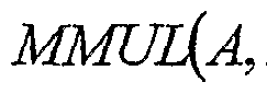
  • MMUL(A,B) A * B * 2- n m dN Which yields a reduced result , i.e., 0 ⁇ MMUL(A, B) ⁇ N .
  • bits of integer values such as the n- bit integer A ⁇ (A n _ l ,...,A i , A Q ) 2 , are represented utilizing the notation
  • An algorithm for computing Montgomery multiplication (in radix 2) can be carried out by the following steps:
  • Step 1.4 called herein the reduction step, is an essential step without which the output of the algorithm, S , is not necessarily reduced.
  • A,B ⁇ N as assumed, it can be shown (by induction) that before the reduction step (1.4) the result, S, is bounded by N + B .
  • This Montgomery multiplication algorithm which computes MMUL(A,B) can be used for computing the regular modular multiplication A * B modN . This can be carried out in more than one way, as illustrated in the following steps: Method 1:
  • Method 2 involves the computation of auxihary values, A' and 5' . This transforms the integers A and 5 to what is called the "Montgomery base”. The first Montgomery multiplication is applied to the transformed numbers, resulting in:
  • Method 1 (computing the auxiliary value) is the main reason for which the Montgomery algorithm is not necessarily considered useful for computing a single modular multiplication, in comparison with a direct approach.
  • Method 2 can be used efficiently when several modular multiplications are required. After converting the input to the Montgomery base, all multiplications are performed by means of the Montgomery multiplication algorithm, and the result is converted to the regular base at the end of the multiplications sequence. In such cases, the computational overhead of Method 2 is negligible, and the Montgomery algorithm substantially improves the efficiency in the overall calculations.
  • the most typical example is the computation of the modular exponent A E modN (for an 7n-bit integer value exponent E , where with no lose of generality, we assume here that A ⁇ N), utilizing Method 2 and the Montgomery multiplication.
  • the exponentiation result can be computed, for example, as described hereinbelow (left-to -right binary exponentiation):
  • the computation of the pre-calculated value A' A * 2" modN (0 ⁇ .4' ⁇ N) converts the input to the Montgomery base
  • the Montgomery multiplications and squaring (steps 2.1 and 2.2) correspond to the sequence of multiplications and squaring that implement the left-to-right binary exponentiation in the regular base
  • the Montgomery multiplication by 1 (step 2.3) converts the result back to the regular base.
  • Reduction (step 1.4) in intermediate steps, in each Montgomery multiplication implemented by algorithm 1, is required in order to make sure that the result remains bounded by N .
  • the reduction is of vital importance in implementation of such chained algorithms, since it assures that the input to the subsequent Montgomery multiplication is properly bounded. If reduction is not performed, and the result of one Montgomery multiplication (without the reduction step) exceeds N, overflow or erroneous results may occur in subsequent steps.
  • the main advantage in using the Montgomery multiplication lies in the hardware implementation of this multiplication operation.
  • Example 2 Table 2 illustrates the calculation of A E modN , for n-bits values A and N, and the -bit value E, utilizing the algorithm herein above.
  • the value obtained in the preceding step 7 (/+1) is followed by the result obtained in step 2.1 ⁇ 1+1 , and the result obtained in step 2.2, T ⁇ y
  • A 212
  • N 249.
  • the Montgomery multiplication MMUL(A,B) is utilized for the calculation of Montgomery multiplication, Montgomery square, and Montgomery multiplication by 1.
  • the accumulated result may be greater than N, and reduction may be required in order to obtain the (correctly reduced) results of the Montgomery multiplication.
  • Dedicated circuitry is required for detecting the cases where the result is greater than N, and for performing the appropriate subtraction (i.e., the required reduction).
  • the additional storage of A, 2* A and 3* ⁇ may be bypassed at the cost of (cumbersome) setting the hardware control accordingly: adding 2* A may be implemented by shifting the stored value of A and then feeding it to the accumulator, and adding 3*A may be implemented by adding the value of A and the shifted value of A to the accumulator.
  • Analogous methods use larger values of m, more storage or hardware/control, but a smaller number (l+[k/m]) of iterations.
  • scanning m bits of M and L in each iteration yields 2 2m combinations for the quantity that is to be added.
  • Storage of 15 quantities is needed unless extra hardware/control is used for adding 2(A+B) and/or adding S(A+B) by using the stored value of (A+B).
  • the apparatus depicted in Fig. 1 utilizes three registers R0, Rl, and R2, a 1:4 multiplexer (MUX), and a Carry Save Adder (CSA), to carry out the calculation of A*B+C*D+G.
  • the registers R0 and R2 are n.-bits each, while register Rl is of n+1 bits.
  • Each of the registers, R0, Rl, and R2 is connected to one of the MUX's inputs, In2,In3, and Inl , respectively, while the MUX's input InO is constantly fed by a "0" value (an n-bit value).
  • the multiplexer MUX has two control inputs, CO and Cl, such that for each state of the control inputs, CO and Cl, a corresponding input is selected, and output on the MUX's output (out).
  • the CSA is of n+2 bits, to allow over flow of 2 bits, and it is utilized for adding the- value of the selected input (InO,I ⁇ l,In2, or In3), retrieved via the MUX's output out, to its present content.
  • the result of this addition is stored in the CSA, which is then subject to a right shift performed to the CSA content. Shifting the bits of an even binary value to the right is equivalent to the division of that value by 2 (in step 1.3 above).
  • the following operations are performed: ⁇ 1) selection of the respective value on InO, Inl, In2, and In3 ;
  • bits (MSB) of the calculated result, and another n LSBs, of the calculated result, are obtained on the CSA 0 output, during the iterations.
  • serial approach The main drawback of the serial approach is that it is time- consuming (the addition of n+1 cycles is required to obtain the CSA content). On the other hand, although performance is significantly improved utilizing the parallel approach, it is considered costly in terms of hardware means.
  • This apparatus is efficiently utilized to perform Montgomery multiplication by applying the Montgomery method, as described in Patent Application WO 98/50851 and US 6,185,596.
  • This method requires testing, after each iteration of the Montgomery process, if the addition result exceeds the modulus value N. In such cases, the result does not exceed 2 *N . Consequently, dedicated hardware is utilized in those implementations for testing the result in each iteration, and for subtracting the modulus value N from the result, whenever it exceeds the modulus value.
  • the present invention is directed to a method for carrying out modular arithmetic computations involving multiplication operations by utilizing a non-reduced and extended Montgomery multiplication between a first A and a second B integer values, in which the number of iterations required is greater than the number of bits n of an odd modulo value N, the method comprising: a) providing an accumulating device (S) capable of storing n+2 bit values, of adding n+2-bit values (X) to it content (S + X ⁇ S), and of dividing its content by 2 (S/2 ⁇ S ); b) whenever desired, setting the content of the device to a zero value ("0"- - S) an performing in the device at least s(>n+l) iterations, while in each iteration choosing one bit, in sequence, from the value of the first integer value A (A ⁇ ;0 ⁇ I ⁇ s ⁇ l ), starting from its least significant bit
  • a j and the second integer value B (S + A j * B - S); b.2) adding to the resulting content of the device the product of its current least significant bit S 0 and N (S + S Q * N ⁇ S); b.3) dividing the resulting content of the device by 2 (572 - S); and b.4) obtaining a non-reduced and extended Montgomery multiplication result by repeating steps b.l) to b.3) s-1 additional times while in each time using the previous result (S).
  • the Montgomery multiplication result can be obtained by unifying steps b.l) to b.3) into a single step, by providing a first storing device (R2) for storing the modulo value N, a second storing device (R0) for storing the value of the second integer B, a third storing device (Rl) for storing the sum of the modulo N and the second integer value B, providing an arbitration circuitry having a first (Inl), second (In2) and third (In3), inputs from the first (R2), second (R0) and third (Rl), storage devices respectively, and having an additional zero input (InO), the arbitration device receives a first (Cl) and a second (CO) control inputs, and is capable of selecting one of its other inputs as it output, such that: whenever its first (Cl) and second (CO) control inputs are zero, selecting the additional zero input (InO); whenever its first control input (Cl) is one and its second control input (CO) is zero, selecting its second input (In2); whenever its first
  • the computation is carried out by applying the bits of the first integer value A (A t ;0 ⁇ I ⁇ s), one by one, in sequence, starting from its least significant bit (A Q ), to the first control input (Cl), and providing circuitry for producing the state (K j ) of the second control input (CO) according to the state of the selected bit of the first integer value (A t ), the state of the least significant bit of the second integer value (5 0 ), and according to the state of the least significant bit of the accumulating device (S 0 ).
  • the state of the second control input (CO) can be produced by circuitry comprising a logical AND gate, and a logical XOR gate, where the inputs of the logical AND gate are receiving the states of the first control input (Cl) and the state of the least significant bit (5 0 ) of the second integer value B, and where the inputs of the logical XOR gate are receiving the output from the logical AND gate and the state of the least significant bit of the accumulating device (S Q ), and where the output of the logical XOR gate is utilized as the state of the second control input (CO).
  • the number of iterations s utilized for carrying out the Montgomery multiplication is n+2, thereby an extended Montgomery multiplication result is obtained, in which n+2 iterations are performed.
  • the method may further comprise allowing modular arithmetic operations to be carried out, by utilizing for the first (R2), second (RO), and third (Rl) storage devices an n+2 bits shift registers having a serial input into their most significant bit locations, and which may be capable of outputting their content in parallel, providing the first storage device (R2) with a serial output, from its least significant bit location (R2 ⁇ ), and allowing it to perform cyclic bit rotation, allowing the second storage device (R0) to receive on its serial input the least significant bit (S 0 ) of the accumulating device, providing a fourth storage device
  • the accumulating device consist of n+2 addition and latching stages, each of which consists of a first and a second flip flop devices and a full adder device having three inputs, except for the first stage wherein the second flip flop is excluded.
  • the first input of the full adder is connected to the output of a first flip-flop device
  • the second input of the full adder is connected to the output of a second flip flop device of the subsequent addition and latching stage
  • the third input of the full adder is connected to the respective bit output of the arbitration device (MUX, ⁇ i ⁇ n + 1).
  • the method may further comprise adding the output from the third arbitration device (MX3), via the serial input of the accumulating device, to the addition result of the ( ⁇ +l)-th addition and latching stage by providing the (rc+lj-th addition and latching stages with a first and second half adder devices, and a third flip flop device, connecting the input of the first flip flop device to the sum output of the second half adder, connecting the input of the second flip flop device to the carry output of the second half adder, and connecting the output of the flip flop device to the second input of the full adder of the (n+2)-th addition and latching stage, connecting the first input of the second half adder to the carry output of the full adder of the (n.+l)-th addition and latching stage, and it second input, to the carry output of the first half adder, connecting the first input of the first half adder to the sum output of the full adder, and connecting the second input of the second half adder to the output of the third arbitration device (MX3); and
  • the state of the second control input (CO) can be determined utilizing the least significant bit of the second storage device (R0), the output of the fourth arbitration device (MX4), the carry output of the full adder of the first addition and latching stage, and the sum output of the full adder of the second addition and latching stage.
  • the least significant bit of the second storage device (RO) and the output of the fourth arbitration device (MX4) is carried out by connecting the least significant bit of the second storage device (RO) and the output of the fourth arbitration device (MX4), to the inputs of an AND logical gate, providing an additional half adder and an additional flip flop device, connecting the first input of the half adder to the sum output of the full adder of the second addition and latching stage, and its second input to the carry output of the full adder of the first addition and latching stage, connecting the sum output of the half adder to the input of the additional flip flop device, and connecting the output of the AND logical gate and the output of the flip flop device to the inputs of a XOR gate, and utilizing the output of the XOR gate to determine the state of the second control input (CO).
  • RO the least significant bit of the second storage device
  • MX4 arbitration device MX4 arbitration device
  • the method may further comprise carrying out non-reduced Montgomery squaring of an integer value B, by loading the first (R2), second (RO), and third (Rl), storage devices with the values of the modulus N, the integer B, and the sum of the modulus and the integer (N+B), respectively, setting the first (MX1), second (MX2), third (MX3) and fourth (MX4), arbitration devices to select the inputs of the circuitry for producing the state (K ⁇ ) of the second control input (CO), the circuitry for producing the state (K j ) of the second control input (CO), the zero value ("0"), and the output of the sixth storage device (RS), respectively, loading the content of the sixth storage device (RS) with the content of the second storage device (RO), and loading the content of the accumulating device with a zero value, performing the non-reduced and extended Montgomery multiplication wherein the content of the sixth storage device (R5) is shifted by one bit to the right in each cycle, and obtaining the non-reduced Montgomery
  • the method may also comprise carrying out Montgomery multiplication of a first (A) and second (B) integer values, by loading the first (R2), second (RO), third (Rl), and fourth (R3) storage devices with the values of the modulus N, the second integer (B), the sum of the modulus and the second integer (N+B), and the first integer (A), respectively, setting the first (MX1),, second (MX2), third (MX3) and fourth (MX4), arbitration devices to select the inputs of the circuitry for producing the state (K t ) of the second control input (CO), the circuitry for producing the state (K ; ) of the second control input (CO), the zero value ("0"), and the output of the fourth storage device (R3), respectively, loading the content of the accumulating device with a zero value, performing the non-reduced and extended Montgomery multiplication wherein the content of the fourth storage device (R3) is shifted by one bit to the right in each cycle, and obtaining the non-reduced Montgomery multiplication result in the
  • E' (e 0 ,e l ,...,e m _ 2 ) 2 , loading the content of the first, second, third, and fifth, storage devices with the values of the modulus JV, the adjusted operand (A' ), the sum of the modulus and the adjusted operand (N + A'), and the adjusted exponent value E' , respectively, obtaining the bit length m of the exponent value E and performing the following steps m-1 times:
  • the modular exponentiation result is obtained by performing non-reduced and extended Montgomery multiplication of the content of the second storage device (RO) by 1 to obtain the final reduced result in the accumulating device.
  • the method may further comprise carrying out modular multiplication of a first
  • the present invention is directed to an apparatus for carrying out extended and non-reduced Montgomery multiplication of a first (A) and second (B) integer values, in which the number of iterations (s) required is greater the number of bits (n) in the modulo value (N), and in which the Montgomery multiplication result is smaller than twice the modulo value (2xIV), comprising: a first storage device (R2) for storing the modulo value (N); a second storage device (RO) for storing the value of the first integer values (A); a third storage device (Rl) for storing the sum of the first integer value and the modulo (A+N); an arbitration circuitry having a first (Inl), second (In2) and third (In3), inputs from the first (R2), second (RO), and third (Rl), storage devices, and having a fourth input which is zero ("0"), the arbitration
  • the circuitry utilized for producing the state (K j ) of the second control input comprises:
  • the first (R2), second (RO), and third (Rl) storage devices can be n+2 bits shift registers having a serial input into their most significant bit locations, and which may be capable of outputting their content in parallel.
  • the first storage device (R2) may also have a serial output, from its least significant bit location (R2 0 ), allowing it to perform cyclic bit rotation.
  • the accumulating device may consist of n+2 addition and latching stages, each of which consists of a first and a second flip flop devices and a full adder device having three inputs, except for the first stage wherein the second flip flop is excluded, comprising: a) means for connecting the first input of the full adder to the output of a first flip-flop device; b) means for connecting the second input of the full adder to the output of a second flip flop device of the subsequent addition and latching stage; and c) means for connecting the third input of the full adder to the respective bit output of the arbitration device (MUX t 0 ⁇ i ⁇ n + l).
  • the accumulating device may further comprise means for adding the output from the third arbitration device (MX3), via the serial input of the accumulating device, to the addition result of the (n+l)-th addition and latching stage, comprising: a) a first and second half adder devices, and a third flip flop device; b) means for connecting the input of the first flip flop device to the sum output of the second half adder; c) means for connecting the input of the second flip flop device to the carry output of the second half adder, and for connecting the output of the flip flop device to the second input of the full adder of the (n+2)-th addition and latching stage; d) means for connecting the first input of the second half adder to the carry output of the full adder of the (n+l)-th addition and latching stage, and it second input, to the carry output of the first half adder; e) means for connecting the first input of the first half adder to the sum output of the full adder, and for connecting the second input of the second half
  • the state of the second control input (CO) is can be determined utilizing the least significant bit of the second storage device (RO), the output of the fourth arbitration device (MX4), the carry output of the full adder of the first addition and latching stage, and the sum output of the full adder of the second addition and latching stage, comprising: a) means for connecting the least significant bit of the second storage device (RO) and the output of the fourth arbitration device (MX4), to the inputs of an AND logical gate; b) an additional half adder and an additional flip flop device; .
  • Fig. 1 is a block diagram schematically illustrating a prior art apparatus for carrying out multiplication and addition operations
  • Fig. 2 is a block diagram schematically illustrating a preferred embodiment of the invention for computing a non -reduced and extended
  • Fig. 3 schematically illustrates one preferred embodiment of the invention for generating the i bit
  • Fig 4 is a block diagram schematically illustrating a preferred embodiment of the invention for carrying out modular arithmetic operations, utihzing Montgomery multiplication;
  • Fig 5 schematically illustrates a process for computing interleaved
  • FIG. 6A and 6B schematically illustrates a possible embodiment of a CSA device according the method of the invention.
  • Fig 7A and 7B are flowcharts illustrating methods for carrying out exponentiation by utilizing the PKI apparatus.
  • the present invention refers to a method and apparatus for carrying out modular arithmetic operations, which is fast and efficient in terms of hardware means.
  • At the core of the preferred embodiment of the invention is the computation of the • modular multiplication of two integers A and B modulo N (hereinafter A ⁇ B mod N), based on a modified (extended) Montgomery method.
  • NRMM ⁇ S (A,B) will be used hereinafter to denote NRMM ⁇ S) ⁇ A,B,N) .
  • NRMM ⁇ (A,B) The computation of NRMM ⁇ (A,B) is carried out by repeating steps 1.1, 1.2, and 1.3, s( ⁇ n) iterations, without performing the reduction step 1.4.
  • the result of such computation is also termed as non-reduced and extended Montgomery multiplication. It is important to note that the result obtained by this non-reduced and extended Montgomery multiplication is not necessarily reduced (i.e., NRMM ⁇ (A, B,N) may be greater that the modulus N).
  • N is an n-bit integer with A, B ⁇ 2*N, N is odd, and s ⁇ n)
  • a E modN can be implemented by means of a sequence of Montgomery multiplications and Montgomery squaring.
  • a MMUL(A, A) operation with an n bits long operand A (A ⁇ N) may produce a non-reduced result larger than N but smaller than 2*N .
  • an implementation" of (n+2) bits accumulator (CSA) may be utilized according to the method of the invention.
  • the computation of the non reduced extended Montgomery multiplication is implicitly based on adding the value K ⁇ N (for some K ⁇ 0 ' ) to the product A * B .
  • the value of K is not known in advance, and is constructed iteratively. In the preferred embodiment of the invention, in each iteration of the process, another bit K j of the integer K is computed, as will be described hereinafter.
  • the modulus value N may be added to the product of A * 5 any number of times, and could still be considered as the same result modulo N, that is, the result after adding K*N yields the same residue modulo IV if it is reduced to the range [0, N).
  • the value of K is chosen in away that A * B + K *N is divisible by 2 s .
  • the result may be always divided by 2, without a remainder (i.e., by a right shift).
  • a modification of the classical Montgomery multiplication method is utilized to facilitate implementations for modular arithmetic computations, which can be realized completely by hardware.
  • the computation of B) A * B * 2 ⁇ " modN is obtained in a process of n iterations, wherein n is the number of bits in the modulus N.
  • n is the number of bits in the modulus N.
  • the exponentiation process A E modN (A ⁇ N) can be implemented by means of a sequence of Montgomery multiplications and Montgomery squaring (MMUL(X,A), MMUL(X,X)) operations, that even with an n bits long operand X (X ⁇ N), and certainly with an n+1 bits operand X ⁇ 2 * N , may produce a non-reduced result larger than N but smaller than 2 * N .
  • the CSA can provide the CSA[ (603) output which is used to speed up the process of producing the K ⁇ bit. This realization can . be easily implemented in hardware.
  • FIG. 2 An apparatus based on the determination of K j , according to a preferred embodiment of the invention, is illustrated in Fig. 2.
  • An additional shift register, R3, is used in this apparatus for feeding the A ⁇ bits of A .
  • the CSA which is of s+2 bits, acts as an additional storage device, and thus there is no need for an additional storage device for partial results that are obtained in intermediate steps.
  • the value of ' K ⁇ is realized from the values of A s , R0 0 , and CSA[ (603).
  • the value of K j is realized utihzing appropriate circuitry 602 (for which a possible implementation is illustrated in Fig. 3), which receives A ; , i?0 0 , and CSA[ , as inputs.
  • the bit 5 0 is placed in a latching device 200, which receives the LSB of register RO (R0 0 ).
  • Fig. 3 demonstrates one possible implementation of a circuitry 602 for providing the K j bit.
  • the realization in Fig. 3 is carried out utilizing an AND gate 300 and an Exclusive Or (XOR) gate 301, wherein the inputs of the AND gate are the bits A j and 5 0 , and the XOR gate inputs are the output of the AND gate 300, and CSA[ 603.
  • the CSA[ 603 output from the CSA produces an expected value for the CSA LSB, and therefore speeds and simplifies the realization of the K j bit.
  • the method of the invention is utilized for a fast and efficient computation of the extended and non-reduced Montgomery multiplication , wherein A and B are smaller than 2 * N , and N is up to n bits (and s ⁇ n + 2).
  • This apparatus can be modified to allow modular products computation of integers, which have more the n-hits, which is also known as the Montgomery interleaved modular multiplication, as will be discussed later.
  • Fig. 4 depicts an apparatus, according to a preferred, embodiment of the invention, for carrying out arithmetic operations based on the extended non- reduced Montgomery modular multiplication.
  • the apparatus also termed Public Key Interface (PKI) herein, is based on 6 registers (each of n+2 bits), R0, Rl, R2, R3, R4, R5 and a Carry Save Adder (of n+2 bits), CSA, with some control (not shown).
  • PKI apparatus is capable of performing various arithmetic and modular arithmetic operations, as will explained hereinbelow.
  • the control input Cl of the MUX is connected to the output of MX4, which acts as an arbitrator for selecting between the serial outputs of registers R3 and R5.
  • Registers R2, R3 and R4 have serial inputs and serial outputs, and are capable of performing cyclic bit rotation.
  • the other MUX control input, CO is connected to the output of MX1, which acts as an arbitrator to select the input value from register R4, or from the circuitry that produces the value K j .
  • the register R4 has a serial input, which is connected to the output of MX2, which acts as an arbitration for selecting between the input of the CSA 0 value, the output of R4 (useful when cyclic bit rotation of R4 is performed), or the value of K ⁇ 602.
  • the third multiplexer, MX3, selects the input to the CSA serial input, and may select a "0" value or the output of MX4.
  • register R5 is utilized only for carrying out squaring operations which are involved in more complex arithmetic computations (i.e., exponentiation).
  • register R5 is loaded with the content of register R0. Therefore, one may implement the same apparatus without register R5, and read the subsequent bits of register R0 utilizing multiplexing techniques.
  • a possible embodiment of the CSA is illustrated in Figs. 6A and 6B.
  • the CSA illustrated in Figs 6A and 6B is based on a serial approach, wherein a set of n Full Adders (FA) are serially connected.
  • the CSA 600 depicted in Fig. 6A is an n bits CSA, in which each FA has 3 inputs, and 2 outputs, a Carry (C) and Sum (S), each of which is the input of a Flip-Flop (FF) device.
  • Each FA receives the following inputs: the output of the FF which receives the S output of the subsequent FA; the output of the FF which receives its own C output, and a corresponding input from the MUX (MUX, ⁇ , MUX tract -2 ,..., MUX 0 ). In this way, the right-shift of the CSA content, and the addition of the MUX output, out, are effected.
  • the leftmost FA device 610 receives an input from another two stages, 611 and 612, depicted in Fig 6B.
  • the additional stages, 611 and 612, depicted in Fig. 6B are utilized to expand the n bit CSA 600 of Fig. 6A, into a (n+2) bit CSA.
  • the n-th stage 611 in Fig. 6B is utilized for the addition of MX ⁇ I ⁇ * 2" to the CSA content.
  • MX ⁇ I ⁇ * 2 the addition of 4 bits is performed by the n-t . stage 611, it should be understood that in practice only 3 bits are summed by this stage. More particularly, when performing the Montgomery based computations, the input received from MX3 is always in zero state, and when performing regular multiplication, which are part of an interleaved multiplication, the input received from the (n+ ⁇ )-th stage 612 is in zero state.
  • the C output 604 of the first stage FA, and the S output 608 of the second stage FA are connected to the Half Adder (HA) 607 which its S output is connected to a FF from which the output CSA[ 603 is provided for the circuitry utilized for determining K, .
  • the HA 607 may be replaced by a logical XOR gate, or any device capable of realizing the ⁇ operation (i.e., base 2 modular addition).
  • the serial output of the_ CSA, CSA 0 is not provided via an FF device, but instead it is obtained directly from the ⁇ 9 output of the first stage's FA.
  • K J LSB(CSA + R5 J * R0 0 )
  • the control inputs of MXl, MX2, MX3, and MX4 are set to select the input of K ⁇ , K j , "0", and R5 respectively. It should be noted that for this computation the input selection made for MX2 does not affect the result.
  • the control input of MX3 is set to select the R4 input.
  • the value of K is obtained in the R4 register.
  • the content of R5 may be loaded (Fig. 5) with the content of register RO, utilizing conventional parallel/serial techniques (not illustrated) or by software.
  • the NRSQR process may be utilized to compute (B * B + K* N+ CSA)/2 S , or ⁇ B* B + K* N)l 2 S by zeroing the content of the CSA in the initialization steps.
  • the control inputs of MXl and MX4 are set to select the inputs of K j and R3, respectively.
  • the control inputs of MX2 and MX3 are set to select the inputs of Kj and "0", respectively, when a simple NRMM ⁇ is performed, or alternatively, the input of K ⁇ and R4, respectively, as part of an interleaved multiplication
  • K o LSB ⁇ CSA + R0 0 )
  • the control inputs of MXl, MX3, and MX4 are set to select the input of K f , "0", and R3 respectively (the selection of MX2 does not affect this operation).
  • the value of K is obtained in the R4 register, and the final result is obtained in the CSA, as the s cycles of the calculation are finished.
  • an external control may be utilized for forcing "1" at the MX4 output, at the first cycle, and "0" at the remaining cycles (illustrated by dashed lines in Fig. 4).
  • the computation of (B + K * N)/2 S can be obtained by zeroing the content of the CSA in the initialization steps.
  • R4 R4/2 + CSA 0 *2"- 1
  • the control inputs of MXl, MX2, MX3, and MX4 are set to select the inputs of R4, CSA Q , "0", and R3, respectively. After performing n iterations, the n LSBs of the result are obtained in the register R4, and n MSBs of the result are obtained in the CSA. Montgomery exponent
  • the PKI apphcation of an exponent calculation is based on the exponent process that was described hereinabove, for computing.
  • a E modN A ⁇ N with no lose of generality.
  • R4 ⁇ 1 than O ⁇ CS.
  • R0 NRMM ⁇ S) (R0,R3) .
  • Rl R0 + R2
  • a sequence of Montgomery squaring and multiplication are performed in the loop, i the above process.
  • the operation of the PKI apparatus utilizing process 2 is further illustrated in Fig 7A, in a form of a flowchart.
  • the operation is initiated in steps 730 and 731, in which the values A',E N, and m -1 are input to the PKI apparatus.
  • a sequence of operations (steps 4.1. to 4.3. here above) are performed in a loop starting in steps 732a and 732b, where a right shift is performed to the content of register R4, the CSA content is zeroed, and an NRMSQR ⁇ s) of the content of RO is performed.
  • step 732c the NRMSQR ⁇ s) result, which is obtained in the CSA, is loaded into register RO, and the addition result of the content of the CSA and the register R2 is loaded into register Rl.
  • step 732d The operation of step 4.3. of the exponent process hereinabove is carried out in step 732d, where the LSB of R4 is examined, and if it equals "1" the CSA content is zeroed and a NRMM ⁇ of the content of registers RO and R3 is performed, the result of which is then stored in RO and also added to the content of R2 and stored in the register Rl.
  • step 732e the value of the loop index i is decrement by 1, and in step 732f it is checked if the loop index i equals zero.
  • i is not zeroed another iteration of the process is performed, as the operation is proceeded in step 732a, otherwise, the CSA content is zeroed and a MMULBYl ⁇ operation is performed to the content of RO.
  • the exponentiation (reduced) result is obtained in the CSA after performing the MMULBYl ⁇ operation to eliminate the 2 s element.
  • Fig. 7A is carried out utilizing an external control (not shown). This control may be performed by software utilizing a processor/controller, or by the addition of dedicated hardware.
  • R0 NRMM s) (R0,R3)
  • R1 R0 + R2
  • Fig.7B The PKI operations in this process are illustrated in Fig.7B.
  • This process is initiated in steps 750 and 751, in which the values A',E',N, and m-1, are input to the PKI apparatus, and a Flag is set to "1".
  • the operations performed in steps 5.1. to 5.4. in the exponent process here above begins in step 752a, in which a right shift is performed to the content of register R4.
  • step 752b the LSB of R4 is examined, and if it equals "1" another test is performed in step 752c, to determine if the Flag is in the state of "1". If the Flag state is "1", register R3 is loaded with the content of register RO, and the flag state is reset to "0".
  • step 752c the CSA content is zeroed and a NRMM ⁇ operation is performed to the content of registers RO and R3, the result of which is obtained in the CSA, and which is then loaded into the R3 register. The operation continues by passing the control to step 752d.
  • step 752b the operation proceed in step 752d, where the CSA content is zeroed and a NRSQR ⁇ operation of the content of RO is carried out, the result of which is obtained in the CSA.
  • the NRSQR ⁇ result is then loaded into register RO, and it is also added to the content of register R2.
  • the addition result of the contents of the CSA and register R2 is stored in register Rl.
  • step 752f the loop index i is decrement by 1.
  • step 752e i is examined to determine if it equal zero. If i is not zeroed, another iteration is performed as the control is passed to step 752a.
  • the CSA content is zeroed and a NRMM ⁇ operation of the RO and R3 contents is performed, the result of which is obtained in the CSA, and loaded into register RO.
  • the addition of the contents of register R2 and the CSA is stored in register Rl, the CSA content is zeroed and a MMULBYl ⁇ is performed.
  • the final result (reduced) is then obtained in the CSA.
  • the method of the invention substantially improves the security of the PKI apparatus, particularly against attacks, which are based on the detection of subtraction operation, as performed in the conventional Montgomery Multiplication methods.
  • attacks which are based on the detection of subtraction operation, as performed in the conventional Montgomery Multiplication methods.
  • the user's secret (private) key is computed by revealing the reduction operations performed (W. Schindler "A Timing Attack against RSA with the. Chinese Reminder Theorem", Second International Workshop Worcester, MA, USA, August 2000).
  • a common method, which is currently used, against such attacks is to perform additional (dummy) subtraction operations, which of course consumes more time and power. Since in the method of the invention subtractions are not performed, it is not possible to reveal the secret key utilizing such methods.
  • the method of the invention can be utilized to implement a right-to-left exponentiation process with two PKI apparatus operating in parallel.
  • a parallel implementations further improves the security of the system. Since it is difficult to follow and identify when and which operations are performed by such a parallel system, the opponent task becomes even more problematical.
  • Fig 5 the values loaded into each register (RO, Rl, R2, R3, and R4), and the input selection of each of the multiplexers (MXl, MX2, MX3, and MX4), are described, for different steps (1,11, III, and IV) of the Montgomery interleaved multiplication.
  • the registers are loaded with the respective values, the MUXs control input is set to provide the corresponding input, and a process of s iterations is performed, for calculating the respective product.
  • each integer may consist of I partial values, each of which is of n-bit.
  • step I the computation of A 0 * B° +N° *K° )/2 ⁇ " is performed by loading registers RO, Rl, R2, and R3, with 5°,5 0 + N 0 ,N° , and A 0 , respectively.
  • the control inputs of MXl, MX2, MX3., and MX4 are set to select the inputs of K j , K J , "0", R3, respectively.
  • a 0 * 5° * 2 ⁇ * modN 0 remains in the CSA. Since in this step MX2 selects the K ⁇ output, register R4 is -loaded with bits of the K° value, which are required for the computation of the next step.
  • step II regular multiplication is performed, to calculate 4° - 5 1 + N 1 - K° + CSA ( j wherein CSA ⁇ is the result that was obtained in the previous step, step I.
  • the values B B l + N N ⁇ , and A 0 are loaded into the R0, Rl, R2, and R3, registers, respectively, and the control inputs of MXl, MX2, MX3 travers and MX4, are set to select the inputs of i? 4 , CSA Q , "0" , R3, respectively.
  • the right shift of the bits of R3 is a cyclic bit rotation, so that there is actually no need to reload R3 with the value of A 0 . Since in this step the apparatus is utilized for the calculation of regular multiphcation, the n LSBs of the result are fed into the serial-in of the R4 register, and the n MSBs of the result remain in the CSA.
  • step III the calculation of
  • LSBs of the result are loaded into the R4 register, and the n MSBs (which may also be of n+1 bits) of the result are obtained in the CSA.
  • steps I to VI may be greater than N, and thus reduction may be required. If it is required, reduction is performed by software after each step. Alternatively, one may implement the same method of interleaved multiplication by utilizing an extended non-reduced approach without needing to reduce the obtained result after each step. In addition, the computation of greater values may be carried out utihzing software for storing temporary result of the interleaved multiphcation.

Landscapes

  • Physics & Mathematics (AREA)
  • Engineering & Computer Science (AREA)
  • General Physics & Mathematics (AREA)
  • Mathematical Analysis (AREA)
  • Mathematical Optimization (AREA)
  • Pure & Applied Mathematics (AREA)
  • Computational Mathematics (AREA)
  • Theoretical Computer Science (AREA)
  • Computing Systems (AREA)
  • Mathematical Physics (AREA)
  • General Engineering & Computer Science (AREA)
  • Complex Calculations (AREA)
  • Hardware Redundancy (AREA)
  • Apparatus For Radiation Diagnosis (AREA)

Abstract

A method for carrying out modular arithmetic computations involving multiplication operations by utilizing a non-reduced and extended Montgomery multiplication between a first A and a second B integer values, in which the number of iterations required is greater than the number of bits n of an odd modulo value N. The method comprises storing n+2 bit values in an accumulating device (S) capable of, of adding n+2-bit values (X) to it content, and of dividing its content by 2. Whenever desired, the content of the accumulating device is set to zero value. At least s(>n+1) iterations of the following steps are performed, while in each iteration choosing one bit, in sequence, from the value of said first integer value A, starting from its least significant bit: adding to the content of the accumulating device S the product of the selected bit and said second integer value B; adding to the resulting content the product of its current least significant bit and N; dividing the result by 2; and obtaining a non-reduced and extended Montgomery multiplication result by repeating these steps s-1 additional times while in each time using the previous result (S).

Description

A METHOD AND APPARATUS FOR CARRYING OUT EFFICIENTLY ARITHMETIC COMPUTATIONS IN HARDWARE
Field of the Invention
The present invention relates to the field of fast and efficient implementation of modular arithmetics in hardware. More particularly, the invention relates to a method and apparatus for carrying out modular arithmetic operations such as modular multiplication and exponentiation, utilizing Montgomery and straightforward methods.
Background of the Invention
The core operations of modern Public Key Cryptosystems (PKC) are typically based on performing modular arithmetic functions, in particular modular exponentiation, where modular exponentiation is essentially based on sequences of modular multiplications and modular squares. Consequently, fast methods for performing modular arithmetic functions, particularly in hardware, are of great importance for practical implementation of PKC. The Montgomery method offers an efficient way of carrying out some modular operations, most important of which is modular exponentiation. The advantage of this method is mostly appreciated in hardware implementations of modular exponentiation. Thus, the Montgomery method is widely adopted in implementations of PKCs that implement, for example, RSA, Digital Signature Standard (DSS), Diffie-Hellman (DF) key exchange, and Elliptic Curve Cryptography (ECC) algorithms (^Handbook of Applied Cryptography" by Alfred J. Menezes, Paul C. van Oorschot and Scott A. Vanstone, CRC Press October 1996).
Montgomery Multiplication, Definition: Given the n- it integers A, B, and N [N > A,B, N is odd), the Montgomery multiplication MMUL(A,B,N,n) , denoted also by MMUL{A,B) (for short), is defined by:
MMUL(A,B) = A * B * 2-n m dN Which yields a reduced result , i.e., 0 < MMUL(A, B)< N .
Notations: In the following discussion, the bits of integer values, such as the n- bit integer A ~ (An_l ,...,Ai , AQ)2 , are represented utilizing the notation
A, (θ ≤ i ≤ n - l), wherein the Most Significant Bit (MSB) An_λ is the leftmost bit, and the Least Significant Bit (LSB) A0 is the rightmost bit, of the integer value
A. Additionally, the value of a given variable S , in the j-th iteration, is denoted by S^ The notations of modular results, such as A * B modJV , refer to their reduced value in the range [0, N).
An algorithm for computing Montgomery multiplication (in radix 2) can be carried out by the following steps:
Algorithm 1:
Input: A, B, N, n (Precondition: A, B, N are n-bit integers, satisfying
N > .4, £ and IV" is odd)
Output: MMUL(A, B) = A *B *2~n mod N
S=0
For I from 0 to n-l do
1.1 S = S + Aj *B
1.2 S = S + SQ * N
1.3 S = S/2 End for
1.4 If S > N Then S = S -N Return S
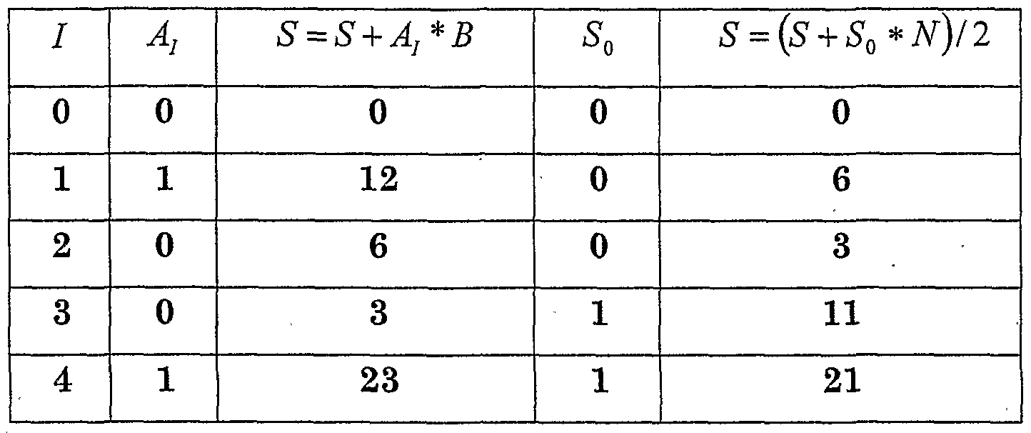
The algorithm main loop requires only a series of additions (steps 1.1 and 1.2) and divisions by 2 (step 1.3). Step 1.4, called herein the reduction step, is an essential step without which the output of the algorithm, S , is not necessarily reduced. Example 1: Table 1 illustrates this process of computing MMUL (A, B) for .4 = 18 = (10010)2 , 5 = 12 = (0110θ)2 , with N = 19 = (10011)2. In this example n = 5 and the Montgomery multiplication is 18 * 12 * 2 ~5 mod 19 = 2
TABLE 1: (Precondition: S = 0 , A = 18 , B = 12 , and N = 19)
Figure imgf000004_0001
Without step 1.4, the output of the algorithm, S , is not necessarily in the range [0, N). In particular, S may be of more than n bits. Thus, the additional reduction (S = S -- N) (step 1.4) is sometimes required in order to shift the algorithm's output to the range [0, N). In Example 1 above, the calculation result is 5" = 21 > JV , and thus the additional reduction _? = .?. - JV = 21 - 19 = 2 is required in this case. In the case where A,B<N, as assumed, it can be shown (by induction) that before the reduction step (1.4) the result, S, is bounded by N + B . Thus, in the cases where S > N , after the iteration steps 1.1, 1.2, and 1.3, the additional reduction step 1.4 (S = S-N), that is performed at most only once, is sufficient to reduce the final result to the range [0, N), and therefore to ensure that the desired result S = A *B * 2 modN is indeed the output of the algorithm.
This Montgomery multiplication algorithm, which computes MMUL(A,B) can be used for computing the regular modular multiplication A * B modN . This can be carried out in more than one way, as illustrated in the following steps: Method 1:
Input: A, B, N, A' (A, B, and N are n.-bit integers, pre-computed value:
A' = A*2" modN)
Output: A*B modN
T = MMUL(A',B) Return T
For example, for the case of A = 18, B = 12 , N = 19, and n=5, the auxiliary value A' = 18 * 25 mod 19 = 6 is pre-computed, and is then used to calculate: T = 1^1011( ,3) = 6 *12*2-5 modl9 = 7
Method 2:
Input: A, B, N, A B' (A, B, and N are n-bit integers, pre-computed values:
A' = A*2" modN and B' = 5* 2" modN)
Output: A*B modN
T = MMUL(A',B') T = MMUL{T,\) Return T
For example, for the case of ^4 = 18, 5 = 12, N = 19, and n=5, two auxiliary values are pre-computed: A' = 18* 25 modl9 = 6 and 5' = 12 * 25 modl9 = 4 which are then used to calculate: T = MMUL(A', B') = 6 * 4 * 2"5 modl9 = 15 and finally, the result is computed by:
T = MMUL(T,l) = 15 * 1 * 2~5 modl9 = 7
Method 2 involves the computation of auxihary values, A' and 5' . This transforms the integers A and 5 to what is called the "Montgomery base". The first Montgomery multiplication is applied to the transformed numbers, resulting in:
T = MMUL (A',B') = A' * B' * 2-" mod N = A * B * 2n mod N
This corresponds to the regular modular multiplication in the regular representation of A and 5 .
The second Montgomery multiplication (by 1) converts the result back to the regular base representation. In other words, it removes the redundant 2" factor from the above result, T = MMUL(Α,B'), thus obtaining the requested result:
T = MMUL{T,1) = (A * B * 2n)*l * 2-" modN = A * B modN
The overhead involved with Method 1 (computing the auxiliary value) is the main reason for which the Montgomery algorithm is not necessarily considered useful for computing a single modular multiplication, in comparison with a direct approach. However, Method 2 can be used efficiently when several modular multiplications are required. After converting the input to the Montgomery base, all multiplications are performed by means of the Montgomery multiplication algorithm, and the result is converted to the regular base at the end of the multiplications sequence. In such cases, the computational overhead of Method 2 is negligible, and the Montgomery algorithm substantially improves the efficiency in the overall calculations. The most typical example is the computation of the modular exponent AE modN (for an 7n-bit integer value exponent E , where with no lose of generality, we assume here that A<N), utilizing Method 2 and the Montgomery multiplication. The exponentiation result can be computed, for example, as described hereinbelow (left-to -right binary exponentiation):
Algorithm 2: Input: A, E, N Output: AE modN
T{m_l) = A' = A * 2n modN For I from m-2 to 0 do
2.1 T(I) = MMUL(T{I+1),T{1+I))
2.2 i f £; = 1 then T{1} = MMUL(T(I),A') End for
23 T{0) = MMUL(T{0),I) Return r(0)
The computation of the pre-calculated value A' = A * 2" modN (0 ≤ .4' < N) converts the input to the Montgomery base, the Montgomery multiplications and squaring (steps 2.1 and 2.2) correspond to the sequence of multiplications and squaring that implement the left-to-right binary exponentiation in the regular base, and the Montgomery multiplication by 1 (step 2.3) converts the result back to the regular base. Reduction (step 1.4) in intermediate steps, in each Montgomery multiplication implemented by algorithm 1, is required in order to make sure that the result remains bounded by N . The reduction is of vital importance in implementation of such chained algorithms, since it assures that the input to the subsequent Montgomery multiplication is properly bounded. If reduction is not performed, and the result of one Montgomery multiplication (without the reduction step) exceeds N, overflow or erroneous results may occur in subsequent steps.
The main advantage in using the Montgomery multiplication lies in the hardware implementation of this multiplication operation. The MMUL algorithm requires, in each step, only the LSB of the accumulating result (step 1.2 above S = S + S0 * N). The following example demonstrates an exponentiation operation carried out utihzing the algorithm described hereinabove. In this example the calculation of 212240 mod249 = 241 is computed.
Example 2: Table 2 illustrates the calculation of AE modN , for n-bits values A and N, and the -bit value E, utilizing the algorithm herein above. In table 2, the value obtained in the preceding step 7(/+1) is followed by the result obtained in step 2.1 {1+1 , and the result obtained in step 2.2, T^y In this example A = 212 , E = 240 = (l l l l0000)2 , and N = 249. Hence, A is of w = 8 bits, E is of m = 8 bits, and the pre-calculated value required is A' = 212 * 28 mod249 = 239.
TABLE 2: (Precondition: A = 212 , E = 240 = (l l l lOOOθ)2 , N = 249 , and T{η) = A' = 239 )
Figure imgf000008_0001
And the final result is obtained by computing r(0) = MA UL(T{0} ,l) = 193 * 1 * 2"8 mod 249 = 241.
In this example, the Montgomery multiplication MMUL(A,B) is utilized for the calculation of Montgomery multiplication, Montgomery square, and Montgomery multiplication by 1. As was previously discussed, before the reduction step (1.4), the accumulated result may be greater than N, and reduction may be required in order to obtain the (correctly reduced) results of the Montgomery multiplication.
In Example 2, for 1=6, δ, and 4, reduction was required in performing I MUL(T(l),A'), and for 1=1 and 6 in performing MMUL(T{M),T{M)) .
It should be noted that the need for reductions substantially complicates hardware realizations of such apparatus, particularly when the number of bits n is significantly large (e.g., τι=512). Dedicated circuitry is required for detecting the cases where the result is greater than N, and for performing the appropriate subtraction (i.e., the required reduction).
Efficient implementations of integer multiplication, achieved by indirect methods that avoid actual multiplication, are known in the literature (e.g., K. Hwang, Computer Arithmetic; Principles, Architecture, and Design, Wiley, New- York, 1979; Chapter 5). Such methods obtain the multiplication result by means of successive additions of appropriately pre-chosen quantities. For example, the value S = S + M * A , where M is of m=2 bits long, can be obtained without directly computing the product M*A, by using only additions of. three pre-stored quantities, as follows. The quantity to be added to the accumulator depends on one of the four possible cases M=(0,0), =(0,1), M=(1,0), M=(l,ϊ): If M=(0,0), nothing is added to the accumulator S. If M=(Q,1), the value A is added to the accumulator S. If M=(1,0), the value 2* A is added to the accumulator S. If =(l,l), the value 3*A = A+2*A is added to the accumulator S.
Thus, the sum S = S + M * A can be obtained in one operation, by identifying the appropriate case (a 1:4 multiplexer in hardware) and adding, accordingly, either 0, A, 2* A or 3*A to the accumulator. The additional storage of A, 2* A and 3*Λ may be bypassed at the cost of (cumbersome) setting the hardware control accordingly: adding 2* A may be implemented by shifting the stored value of A and then feeding it to the accumulator, and adding 3*A may be implemented by adding the value of A and the shifted value of A to the accumulator.
Consequently, optimizing this operation requires balancing between storage and speed/hardware requirements. The extra storage of the values A, 2*A, S*A may be advantageous if the same operation is repeated many times. For example, the computation of S = S + K*A when K is of k bits long, can be achieved iteratively. In each of (l+[k/m]) = (l+[k/2]) iterations, the m=2 next bits of K are scanned and define a temporary value of M ( -bit portions of M), with which the above method is used. The number of bits m, designates the bit length of those temporary values (portions of M), and thus also define the number of right shifts that should be performed to the addition result S = S + K * A . Analogous methods use larger values of m, more storage or hardware/control, but a smaller number (l+[k/m]) of iterations. The same method can be used when the value M*A + L*B is to be added to the accumulator, in order to compute S = S + M*A + L*B . In such case, scanning m bits of M and L in each iteration yields 22m combinations for the quantity that is to be added.
For example, with m=2, the 22*2 =16 combinations for the added quantity are: 0, A, 2*A, 3*A, B, 2*5, 3*5, A + B, A + 2*B, A + 3*B, 2*A + B, 2*(A + B), 2*A+3*B, 3*A + B, 3*A + 2*B ,3*(A + B). Storage of 15 quantities is needed unless extra hardware/control is used for adding 2(A+B) and/or adding S(A+B) by using the stored value of (A+B). For m=l, there are 22*1 = 4 combinations namely: 0, A, B, A+B. The case m=l is illustrated in Fig.1 for carrying out multiplication and summation operations of four integers, A, B, C, and D. The apparatus depicted in Fig. 1 utilizes three registers R0, Rl, and R2, a 1:4 multiplexer (MUX), and a Carry Save Adder (CSA), to carry out the calculation of A*B+C*D+G. The registers R0 and R2, are n.-bits each, while register Rl is of n+1 bits. Each of the registers, R0, Rl, and R2, is connected to one of the MUX's inputs, In2,In3, and Inl , respectively, while the MUX's input InO is constantly fed by a "0" value (an n-bit value).
The multiplexer MUX has two control inputs, CO and Cl, such that for each state of the control inputs, CO and Cl, a corresponding input is selected, and output on the MUX's output (out). The calculation of A * B + C * D + G is carried out by loading registers R0, Rl, R2, and the CSA with the values of D, B+D, B, and G, respectively, and serially feeding the data bits of A and C (A; and C} (l = 0,1,2,..., n-l)), through the MUX's control inputs, CO and Cl respectively.
The CSA is of n+2 bits, to allow over flow of 2 bits, and it is utilized for adding the- value of the selected input (InO,Iήl,In2, or In3), retrieved via the MUX's output out, to its present content. The result of this addition is stored in the CSA, which is then subject to a right shift performed to the CSA content. Shifting the bits of an even binary value to the right is equivalent to the division of that value by 2 (in step 1.3 above). Thus, in each cycle in the operation of this system, the following operations are performed: 1) selection of the respective value on InO, Inl, In2, and In3 ;
2) addition of the selected value with the current content of the CSA register; and
3) right shifting the CSA bits, which also introduce the LSB of the CSA (i.e., CSA0 ) on the CSAQ output.
To implement Steps 1 and 2, the bits of A and C, At and Cy (/ = 0,1,2,..., n -l) , are serially introduced on the MUX's control inputs, CO and Cl, starting with the LSBs. Consequently, the MUX's output out^ may take any of the following values in each and every iteration I OUt(f) =
Figure imgf000012_0001
The process of calculating A * B + C * D + G is further described by the following pseudo-code.
D → R0. B + D → R1. B → R2 .G → CSA For J from 0 to n-l Do
GS4(/+l) = (C^(/) + oMt(/))/2 End For
After n iterations the CSA's content (CSA^_^) holds the n+1 Most Significant
Bits (MSB) of the calculated result, and another n LSBs, of the calculated result, are obtained on the CSA0 output, during the iterations. The CSA's content may be output utilizing a parallel output bus (not illustrated), or alternatively, by resetting the MUX's control inputs (i.e., set C0=Cl=0), and performing n+1 additional iterations, to output the Ji+1 MSBs of the result, on the CSA0 output
(serial approach). The main drawback of the serial approach is that it is time- consuming (the addition of n+1 cycles is required to obtain the CSA content). On the other hand, although performance is significantly improved utilizing the parallel approach, it is considered costly in terms of hardware means.
This apparatus is efficiently utilized to perform Montgomery multiplication by applying the Montgomery method, as described in Patent Application WO 98/50851 and US 6,185,596. In those Patent Applications a precomputed constant (J = -N"1 mod 2") is utilized to calculate in each iteration the number of times, Y = (A * B * j) mod 2" , that modulus N should be added to the multiplication of A * B . This method requires testing, after each iteration of the Montgomery process, if the addition result exceeds the modulus value N. In such cases, the result does not exceed 2 *N . Consequently, dedicated hardware is utilized in those implementations for testing the result in each iteration, and for subtracting the modulus value N from the result, whenever it exceeds the modulus value.
Methods for implementing modular multiplication by using the Montgomery multiplication as known in the art, are mainly affected - in both time and hardware - by the need to reduce the output resulting values, to values which are smaller than N. Furthermore, the reduction step, being dependent on the specific input (via the "if statement) makes this implementation susceptible to (side channels) attacks. Therefore, although the Montgomery multiplication method enables efficient hardware implementation of modular arithmetic operations, such as modular exponentiation, there is a need for improving the hardware implementations of such operations. This may be achieved utilizing a method and an apparatus that does not require repeated reduction after each Montgomery multiplication.
It is an object of the present invention to provide a method and apparatus for carrying out a modified version of Montgomery multiplication in which the intermediate and the final calculation results do not exceed known bounds, and wherein no reduction is required during a chained sequence of such modified Montgomery multiplication, such as the sequence required for an exponentiation process, and the final result of the exponentiation process, is automatically reduced (between 0 and N).
It is another object of the present invention to provide a method and apparatus (called also a PKI apparatus herein) allowing efficient hardware implementations of modular exponentiation, and other modular arithmetic operations, based or not based on the Montgomery multiplication, which include the basic operations required for hardware implementation of public key cryptosystems. It is yet another object of the present invention to provide a method and apparatus allowing efficient hardware implementations of various modular exponentiation algorithms such as right-to -left, left-to-right, m.-array, and sliding- indow exponentiation algorithms.
It is a still further object of the present invention to provide a method and apparatus for a secure PKI apparatus, based on a non-reduced and modified Montgomery multiplication, which is proof against timing attacks.
Summary of the Invention
In one aspect the present invention is directed to a method for carrying out modular arithmetic computations involving multiplication operations by utilizing a non-reduced and extended Montgomery multiplication between a first A and a second B integer values, in which the number of iterations required is greater than the number of bits n of an odd modulo value N, the method comprising: a) providing an accumulating device (S) capable of storing n+2 bit values, of adding n+2-bit values (X) to it content (S + X → S), and of dividing its content by 2 (S/2 → S ); b) whenever desired, setting the content of the device to a zero value ("0"- - S) an performing in the device at least s(>n+l) iterations, while in each iteration choosing one bit, in sequence, from the value of the first integer value A (A} ;0 ≤ I ≤ s ~l ), starting from its least significant bit
( ) b.l) adding to the content of the device S the product of the selected bit
Aj and the second integer value B (S + Aj * B - S); b.2) adding to the resulting content of the device the product of its current least significant bit S0 and N (S + SQ * N → S); b.3) dividing the resulting content of the device by 2 (572 - S); and b.4) obtaining a non-reduced and extended Montgomery multiplication result by repeating steps b.l) to b.3) s-1 additional times while in each time using the previous result (S).
The Montgomery multiplication result can be obtained by unifying steps b.l) to b.3) into a single step, by providing a first storing device (R2) for storing the modulo value N, a second storing device (R0) for storing the value of the second integer B, a third storing device (Rl) for storing the sum of the modulo N and the second integer value B, providing an arbitration circuitry having a first (Inl), second (In2) and third (In3), inputs from the first (R2), second (R0) and third (Rl), storage devices respectively, and having an additional zero input (InO), the arbitration device receives a first (Cl) and a second (CO) control inputs, and is capable of selecting one of its other inputs as it output, such that: whenever its first (Cl) and second (CO) control inputs are zero, selecting the additional zero input (InO); whenever its first control input (Cl) is one and its second control input (CO) is zero, selecting its second input (In2); whenever its first control input (Cl) is zero and its second control input (CO) is one, selecting its first input (Inl); and whenever its first (Cl) and second (CO) control inputs are one, selecting the third input (In3); wherein the selected input is provided as the output of the arbitration circuitry which is attached to the input of the accumulating device. The computation is carried out by applying the bits of the first integer value A (At ;0 ≤ I ≤ s), one by one, in sequence, starting from its least significant bit (AQ), to the first control input (Cl), and providing circuitry for producing the state (Kj ) of the second control input (CO) according to the state of the selected bit of the first integer value (At), the state of the least significant bit of the second integer value (50), and according to the state of the least significant bit of the accumulating device (S0). The state (Kj ) of the second control input (CO) can be produced by producing a value of one (Kj = ) whenever the state of the first control input (Cl) and the state of the least significant bit of the second integer value (50) are one, and the state of the least significant bit of the accumulating device (S0) is zero, or when the state of the first control input (Cl) and the state of the least significant bit (50) of the second integer value B are in different state, and the state of the least significant bit (S0) of the accumulating device is one, otherwise a zero value Kj ="0") is produced as the state (Kj ) of the second control input (CO).
The state of the second control input (CO) can be produced by circuitry comprising a logical AND gate, and a logical XOR gate, where the inputs of the logical AND gate are receiving the states of the first control input (Cl) and the state of the least significant bit (50) of the second integer value B, and where the inputs of the logical XOR gate are receiving the output from the logical AND gate and the state of the least significant bit of the accumulating device (SQ), and where the output of the logical XOR gate is utilized as the state of the second control input (CO).
Preferably, the number of iterations s utilized for carrying out the Montgomery multiplication is n+2, thereby an extended Montgomery multiplication result is obtained, in which n+2 iterations are performed.
The method may further comprise allowing modular arithmetic operations to be carried out, by utilizing for the first (R2), second (RO), and third (Rl) storage devices an n+2 bits shift registers having a serial input into their most significant bit locations, and which may be capable of outputting their content in parallel, providing the first storage device (R2) with a serial output, from its least significant bit location (R2ϋ), and allowing it to perform cyclic bit rotation, allowing the second storage device (R0) to receive on its serial input the least significant bit (S0) of the accumulating device, providing a fourth storage device
(R3) capable of serially outputting it content, bit by bit in sequence (R3j I = 0,1,2,..., n + 1), starting from its least significant bit (R3Q ), the fourth storage device is capable of storing n+2 bits, and of performing cyclic bit rotation to it content, providing a fifth storage device (R4) having a serial input and a serial output, and which is capable of storing values of n+2 bits, providing a sixth storage device (R5) capable of serially outputting it content, bit by bit in sequence (R5j I = 0,1,2,..., n + 1), starting from its least significant bit, the fourth storage device is capable of storing n+2 bits, providing a first arbitration device (MXΪ) having a first input from the fifth storage device (R t), and a second input from the circuitry producing the state of the second control input (K} ), the output of the first arbitration device is attached to the second control input (CO), providing a second arbitration device (MX2) having a first input being equal to the least significant bit of the accumulating device (S0 , and also referred herein as CSAQ), a second input received from the output of the circuitry (Kj ), and a third input connected to the serial output (R4j) of the fifth storage device (R4), the output of the second arbitration device is attached to the serial input of the fifth storage device (R4), providing a third arbitration device (MX3) having a first input which is constantly fed with a zero value ("0"), and a second input received from the serial output of the fifth storage device (R4}), the output of the third arbitration device is connected to a serial input of the accumulating device, providing a fourth arbitration device (MX4) having a first input connected to the serial output of the sixth storage device (R5} ), and a second input connected to the serial output of the fourth storage device (R3j), the output of the fourth arbitration device is connected to the first control input (Cl), and providing an adder capable of performing serial addition of n+2 bit values, the adder receives a first input from the least significant bit location of the accumulating device (S0), and a second input from the serial output of the first storage device (R2), the output of the adder is connected to the serial input of the third storage device (Rl).
Preferably, the accumulating device consist of n+2 addition and latching stages, each of which consists of a first and a second flip flop devices and a full adder device having three inputs, except for the first stage wherein the second flip flop is excluded. In each addition and latching stages the first input of the full adder is connected to the output of a first flip-flop device, the second input of the full adder is connected to the output of a second flip flop device of the subsequent addition and latching stage; and the third input of the full adder is connected to the respective bit output of the arbitration device (MUX, ≤ i ≤ n + 1).
The method may further comprise adding the output from the third arbitration device (MX3), via the serial input of the accumulating device, to the addition result of the (τι+l)-th addition and latching stage by providing the (rc+lj-th addition and latching stages with a first and second half adder devices, and a third flip flop device, connecting the input of the first flip flop device to the sum output of the second half adder, connecting the input of the second flip flop device to the carry output of the second half adder, and connecting the output of the flip flop device to the second input of the full adder of the (n+2)-th addition and latching stage, connecting the first input of the second half adder to the carry output of the full adder of the (n.+l)-th addition and latching stage, and it second input, to the carry output of the first half adder, connecting the first input of the first half adder to the sum output of the full adder, and connecting the second input of the second half adder to the output of the third arbitration device (MX3); and connecting the input of the third flip flop device to the sum output of the first half adder, and connecting it output to the second input of the full adder of the (w-l)-th addition and latching stage. The state of the second control input (CO) can be determined utilizing the least significant bit of the second storage device (R0), the output of the fourth arbitration device (MX4), the carry output of the full adder of the first addition and latching stage, and the sum output of the full adder of the second addition and latching stage. Preferably it is carried out by connecting the least significant bit of the second storage device (RO) and the output of the fourth arbitration device (MX4), to the inputs of an AND logical gate, providing an additional half adder and an additional flip flop device, connecting the first input of the half adder to the sum output of the full adder of the second addition and latching stage, and its second input to the carry output of the full adder of the first addition and latching stage, connecting the sum output of the half adder to the input of the additional flip flop device, and connecting the output of the AND logical gate and the output of the flip flop device to the inputs of a XOR gate, and utilizing the output of the XOR gate to determine the state of the second control input (CO).
The method may further comprise carrying out non-reduced Montgomery squaring of an integer value B, by loading the first (R2), second (RO), and third (Rl), storage devices with the values of the modulus N, the integer B, and the sum of the modulus and the integer (N+B), respectively, setting the first (MX1), second (MX2), third (MX3) and fourth (MX4), arbitration devices to select the inputs of the circuitry for producing the state (K{ ) of the second control input (CO), the circuitry for producing the state (Kj ) of the second control input (CO), the zero value ("0"), and the output of the sixth storage device (RS), respectively, loading the content of the sixth storage device (RS) with the content of the second storage device (RO), and loading the content of the accumulating device with a zero value, performing the non-reduced and extended Montgomery multiplication wherein the content of the sixth storage device (R5) is shifted by one bit to the right in each cycle, and obtaining the non-reduced Montgomery squaring result in the accumulating device. The method may also comprise carrying out Montgomery multiplication of a first (A) and second (B) integer values, by loading the first (R2), second (RO), third (Rl), and fourth (R3) storage devices with the values of the modulus N, the second integer (B), the sum of the modulus and the second integer (N+B), and the first integer (A), respectively, setting the first (MX1),, second (MX2), third (MX3) and fourth (MX4), arbitration devices to select the inputs of the circuitry for producing the state (Kt) of the second control input (CO), the circuitry for producing the state (K; ) of the second control input (CO), the zero value ("0"), and the output of the fourth storage device (R3), respectively, loading the content of the accumulating device with a zero value, performing the non-reduced and extended Montgomery multiplication wherein the content of the fourth storage device (R3) is shifted by one bit to the right in each cycle, and obtaining the non-reduced Montgomery multiplication result in the accumulating device.
The computation of the modular exponentiation AB modN can be carried out by pre-calculating an adjusted operand value ^' = ^4 * 2* modN , composing an adjusted value for the exponent E = { m_l , e m_2 ,..., el } e0 ) by reversing its bit order and eliminating the most significant bit em_ , to obtain the adjusted value
E' = (e0,el,...,em_2)2, loading the content of the first, second, third, and fifth, storage devices with the values of the modulus JV, the adjusted operand (A' ), the sum of the modulus and the adjusted operand (N + A'), and the adjusted exponent value E' , respectively, obtaining the bit length m of the exponent value E and performing the following steps m-1 times:
- right shifting the content of the fifth storage device (R );
- performing non-reduced Montgomery squaring to obtain the non-reduced Montgomery square of the content of the third storage device (R3) in the accumulating device; - loading the content of the third storage device (R3) with the content of the accumulating device; and
- loading the content of the third storage device (Rl) with the sum of the content of the first storage device (R2) and the content of the accumulating device; if the least significant bit (R40) of the fifth storage device equals "1" performing non-reduced and extended Montgomery multiplication to obtain the non-reduced Montgomery multiplication result of the contents of the second storage device (RO) and the fourth storage device (R3), in the accumulating device, loading the content of the second storage device (RO) with the content of the accumulating device, and loading the content of the third (Rl) storage device with the sum of the contents of the first storage device (R2) and the accumulating device accumulating;
After repeating these steps m-1 times the modular exponentiation result is obtained by performing non-reduced and extended Montgomery multiplication of the content of the second storage device (RO) by 1 to obtain the final reduced result in the accumulating device.
Alternatively, the modular exponentiation AE modN can be computed by pre- calculating the adjusted operand value A' = A * 2s modN , loading the content of the first (R2), second (RO), third (Rl), and fifth (R4), storage devices with the values of the modulus N, the adjusted operand (A' ), the sum of the modulus and the adjusted operand (N + A'), and the exponent value E , obtaining the bit length m of the exponent value E, setting a flag to "1", and performing the following steps m-2 times: right shifting the content of the fifth storage device (R ); if the least significant bit (R40) of the fifth storage device equals "1" checking the state of the flag, and if it does not equal "1" performing non- reduced and extended Montgomery multiplication to obtain the non-reduced and extended Montgomery multiplication result of the contents of the second storage device (RO) and the fourth storage device (R3), in the accumulating device, loading the content of the fourth storage device (R3) with the content of the accumulating device, otherwise loading the content of the fourth storage device (R3) with the content of the second storage device (RO) and resetting the state of the flag to "0"; performing extended and non-reduced Montgomery squaring to obtain the extended and non-reduced Montgomery square of the content of the second storage device (RO) in the accumulating device; loading the content of the second storage device (RO) with the content of the accumulating device; loading the content of the third storage device (Rl) with the sum of the content of the first storage device and the content of the accumulating device; After performing these steps m-2 times performing extended and non-reduced Montgomery multiplication to obtain the extended and non-reduced Montgomery multiplication result of the contents of the second storage device (RO) and the fourth storage device (R3), in the accumulating device, loading the content of the second storage device (RO) with the content of the accumulating device, loading the content of the third storage device (Rl) with the sum of the content of the first storage device (R2) and the content of the accumulating device, and performing extended and noή-reduced Montgomery multiplication of the content of the second storage device (RO) by 1 to obtain the final reduced result in the accumulating device.
A modular multiplication of a first (A = Al * 2" + A°) and a second (B = 51 * 2" + 5°) integer values, where the first integer, second integer, and the modulus (N), are of 2 π, bits, can be calculated by computing the Montgomery multiplication (MMUL A°,B )) of the n least significant bits of the first integer value (A0) and of the second integer value (5°), by performing the following steps: loading the first (R2), second (RO), third (Rl), and fourth (R3) storage devices, with the n least significant bits (N°) of the modulus value (TV), the n least significant bits (5°) of the second integer value (B), the sum (5° + N° ) of the n least significant bits of the modulus value (N) and of the n least significant bits (5°) of the second integer value (B), and the n least significant bits (A°) of the first integer value (A), respectively; setting the first (MX1), second (MX2), third (MX3), and fourth (MX4), arbitration devices for selecting the input of the circuitry for producing the state (Kj ) of the second control input (CO), the circuitry for producing the state (K, ) of the second control input (CO), the zero value ("#"), and the fourth storage device (R3) input, and resetting the content of the accumulating device to zero, if it is required; carrying out Montgomery multiplication and obtaining the result (£(/)) in the accumulating device, and the bits state (K, O ≤ I ≤ n -1 ) of the second control input (Kϋ ) in the fifth register (R ); computing the value of A0 * 51 + N1 * K° + S^ of the n least significant bits of the first integer value (A0), the n most significant bits of the second integer value (51), the n most significant bits of the modulus value (Nx),the n-bit value (K°) obtained in the fifth register (R ), and the result obtained in step a) (S^) by performing the following steps: loading the first (R2), second (RO), third (Rl), and fourth (R3) storage devices, with the n most significant bits (N1) of the modulus value (N), the n most significant bits (51) of the second integer value (B), the sum (51 +N1) of the n most significant bits of the modulus value (N) and of the n most significant bits of the second integer value (B), and the n least significant bits (A ) of the first integer value (A), respectively; setting the first (MX1), second (MX2), third (MX3), and fourth (MX4), arbitration devices for selecting the input of the fifth register (R4), the least significant bit of the accumulating device (S0), the zero value ("0"), and the fourth storage device (R3) input; carrying out regular multiplication and obtaining the most significant bits of the result in the accumulating device (S^ ) and the least significant bits of the result in the fifth storage device (i?(4)); computing result of addition of the Montgomery multiplication of the n most significant bits of the first integer value (A1) and the n least significant bits of the second integer value (5°), with the result that was previously obtained (i?4(7/) , S(JJ}), by performing the following steps: loading the first (R2), second (RO), third (Rl), and fourth (R3) storage devices, with the n least significant bits (N°) of the modulus value (IV), the n least significant bits (5°) of the second integer value (B), the sum (5° + N° ) of the n least significant bits of the modulus value (N) and of the n least significant bits (5°) of the second integer value (B), and the n most significant bits (A1) of the first integer value (A), respectively; loading the content of the accumulating device (S, also referred to as CSA herein) with the n least significant bits of the previously obtained result R4^), and loading the content of the fifth storage device (R ) with n most significant bits of the previously obtained result (S^); setting the first (MX1), second (MX2), third (MX3), and fourth (MX4), arbitration devices for selecting the input of the circuitry for producing the state (Kj ) of the second control input (CO), the circuitry for producing the state (K} ) of the second control input (CO), the input from the fifth storage device (R ), and the fourth storage device (R3) input; carrying out Montgomery multiplication and obtaining the result (S^) in the accumulating device, and the bits state (K, O ≤ I ≤ n -1 ) of the second control input (K1 ) in the fifth register (R ); computing A1 * 51 + N1 * Kl + S^ of the n most significant bits of the first integer value (A1 ), the n most significant bits of the second integer value (51 ), the n most significant bits of the modulus value (N1 ), the n-bit value (Kl ) obtained in the fifth register (R ), and the result obtained in step c) (S^) by performing the following steps: loading the first (R2), second (RO), third (Rl), and fourth (R3) storage devices, with the n most significant bits (N1) of the modulus value (N), the n. most significant bits (51 ) of the second integer value (B), the sum (51 + N1) of the n most significant bits of the modulus value (N) and of the n most significant bits of the second integer value (B), and the n most significant bits (A1 ) of the first integer value (A), respectively; setting the first (MX1), second (MX2), third (MX3), and fourth (MX4), arbitration devices for selecting the input of the fifth register (R4), the least significant bit of the accumulating device (S0), the zero value ("0"), and the fourth storage device (R3) input; and carrying out Montgomery multiplication and obtaining the most significant bits of the result in the accumulating device (S^) and the least significant bits of the result in the fifth storage device (R V^ ).
The method may further comprise carrying out modular multiplication of a first
(A = Al * 2' ) and a second (B = B' * 2' ) integer values, where the first
(=0 1=0
integer, second integer, and the modulus N = ∑N' * 2' ), may be of more than
Figure imgf000025_0001
2xn bits, where the computation is carried out by computing intermediate results of the multiphcation of 2xn bits subsequent fractions of the first integer and second integer. In another aspect the present invention is directed to an apparatus for carrying out extended and non-reduced Montgomery multiplication of a first (A) and second (B) integer values, in which the number of iterations (s) required is greater the number of bits (n) in the modulo value (N), and in which the Montgomery multiplication result is smaller than twice the modulo value (2xIV), comprising: a first storage device (R2) for storing the modulo value (N); a second storage device (RO) for storing the value of the first integer values (A); a third storage device (Rl) for storing the sum of the first integer value and the modulo (A+N); an arbitration circuitry having a first (Inl), second (In2) and third (In3), inputs from the first (R2), second (RO), and third (Rl), storage devices, and having a fourth input which is zero ("0"), the arbitration device receives a first (Cl) and a second (CO) control inputs, and thereby is capable of selecting one of it other inputs as it output, that is attached to the input of the accumulating device; circuitry for producing the state (K} ) of the second control input (CO) according to the state of a selected bit of the first integer value (At), the state of the least significant bit of the second integer value (50), and according to the state of the least significant bit of the accumulating device (SQ); and an accumulating device (S) capable of storing n+2 bits values, of adding n+ -bits values (X) to it content (S + X -+ S ), and of dividing it content by 2 (S/2 → S); '
Preferably, the circuitry utilized for producing the state (Kj ) of the second control input comprises:
Circuitry for producing a value of one whenever: the state of the selected bit (Af) and the state of the least significant bit of the second integer value (50) are one, and the state of the least significant bit of the accumulating device (-?„) is zero; or the state of the selected bit (A}) and the state of the least significant bit (50) of the second integer value are in different state, and the state of the least significant bit (S0) of the accumulating device is one; the circuitry produces a zero value in all other cases.
The first (R2), second (RO), and third (Rl) storage devices can be n+2 bits shift registers having a serial input into their most significant bit locations, and which may be capable of outputting their content in parallel. The first storage device (R2) may also have a serial output, from its least significant bit location (R20), allowing it to perform cyclic bit rotation.
The apparatus may further comprise means for allowing modular arithmetic operations to be carried out, comprising: means for connecting the serial input of the second storage device (RO) to the least significant bit (S0) of the accumulating device (S); a fourth storage device (RS) capable of serially outputting it content, bit by bit in sequence (R3j 1 = 0,1,2,...,n + l), starting from its least significant bit (R30 ), the fourth storage device is capable of storing n+2 bits, and of performing cyclic bit rotation to it content; a fifth storage device (R4) having a serial input and a serial output, and which is capable of storing values of n+2 bits; a sixth storage device (R5) capable of serially outputting it content, bit by bit in sequence (R5; I = 0,1,2,..., n + 1), starting from its least significant bit, the fourth storage device is capable of storing n+2 bits; a first arbitration device (MXl) having a first input from the fifth storage device (R4j), and a second input from the circuitry producing the state of the second control input (K} ), the output of the first arbitration device is attached to the second control input (CO); a second arbitration device (MX2) having a first input being equal to the least significant bit of the accumulating device (S0), a second input received from the output of the circuitry (Kj ), and a third input connected to the serial output (R4}) of the fifth storage device (R4), the output of the second arbitration device is attached to the serial input of the fifth storage device (R4); a third arbitration device (MX3) having a first input which is constantly fed with a zero value ("0"), and a second input received from the serial output of the fifth storage device (i?47), the output of the third arbitration device is connected to a serial input of the accumulating device; a fourth arbitration device (MX4) having a first input connected to the serial output of the sixth storage device (R5j ), and a second input connected to the serial output of the fourth storage device (R3} ), the output of the fourth arbitration device is connected to the first control input (Cl); and an adder capable of performing serial addition of n+2 bit values, the adder receives a first input from the least significant bit location of the accumulating device (S0), and a second input from the serial output of the first storage device (R2), the output of the adder is connected to the serial input of the third storage device (Rl).
The accumulating device may consist of n+2 addition and latching stages, each of which consists of a first and a second flip flop devices and a full adder device having three inputs, except for the first stage wherein the second flip flop is excluded, comprising: a) means for connecting the first input of the full adder to the output of a first flip-flop device; b) means for connecting the second input of the full adder to the output of a second flip flop device of the subsequent addition and latching stage; and c) means for connecting the third input of the full adder to the respective bit output of the arbitration device (MUXt 0 ≤ i ≤ n + l).
The accumulating device may further comprise means for adding the output from the third arbitration device (MX3), via the serial input of the accumulating device, to the addition result of the (n+l)-th addition and latching stage, comprising: a) a first and second half adder devices, and a third flip flop device; b) means for connecting the input of the first flip flop device to the sum output of the second half adder; c) means for connecting the input of the second flip flop device to the carry output of the second half adder, and for connecting the output of the flip flop device to the second input of the full adder of the (n+2)-th addition and latching stage; d) means for connecting the first input of the second half adder to the carry output of the full adder of the (n+l)-th addition and latching stage, and it second input, to the carry output of the first half adder; e) means for connecting the first input of the first half adder to the sum output of the full adder, and for connecting the second input of the second half adder to the output of the third arbitration device (MX3); and f) means for connecting the input of the third flip flop device to the sum output of the first half adder, and connecting it output to the second input of the full adder of the (n-l)-th addition and latching stage.
The state of the second control input (CO) is can be determined utilizing the least significant bit of the second storage device (RO), the output of the fourth arbitration device (MX4), the carry output of the full adder of the first addition and latching stage, and the sum output of the full adder of the second addition and latching stage, comprising: a) means for connecting the least significant bit of the second storage device (RO) and the output of the fourth arbitration device (MX4), to the inputs of an AND logical gate; b) an additional half adder and an additional flip flop device; . c) means for connecting the first input of the half adder to the sum output of the full adder of the second addition and latching stage, and its second input to the carry output of the full adder of the first addition and latching stage; d) means for connecting the sum output of the half adder to the input of the additional flip flop device; and e) means for connecting the output of the AND logical gate and the output of the flip flop device to the inputs of a XOR gate, and utilizing the output of the XOR gate to determine the state of the second control input (CO).
Brief Description of the Drawings
In the drawings:
Fig. 1 is a block diagram schematically illustrating a prior art apparatus for carrying out multiplication and addition operations;
Fig. 2 is a block diagram schematically illustrating a preferred embodiment of the invention for computing a non -reduced and extended
Montgomery multiplication;.
Fig. 3 schematically illustrates one preferred embodiment of the invention for generating the i bit;
Fig 4 is a block diagram schematically illustrating a preferred embodiment of the invention for carrying out modular arithmetic operations, utihzing Montgomery multiplication;
Fig 5 schematically illustrates a process for computing interleaved
Montgomery multiplication, according to a preferred embodiment of the invention; Fig 6A and 6B schematically illustrates a possible embodiment of a CSA device according the method of the invention; and
Fig 7A and 7B are flowcharts illustrating methods for carrying out exponentiation by utilizing the PKI apparatus.
Detailed Description of Preferred Embodiments
The present invention refers to a method and apparatus for carrying out modular arithmetic operations, which is fast and efficient in terms of hardware means. At the core of the preferred embodiment of the invention is the computation of the • modular multiplication of two integers A and B modulo N (hereinafter A ■ B mod N), based on a modified (extended) Montgomery method.
A modified (extended) Montgomerv multiplication — definition: For n bits long odd modulus N, integers A, B such that A,B ≤ 2 *N , and an integer s ≥ n , define the Non-Reduced and extended Montgomery Multiplication (NRMM) by
Figure imgf000031_0001
= A * B * 2~s mod(N + ε * N) , where ε = 0 for a reduced result, and ε = 1 for a non-reduced result. For short, when the context (i.e., N and s) is known, NRMM{S)(A,B) will be used hereinafter to denote NRMM{S){A,B,N) . The computation of NRMM^(A,B) is carried out by repeating steps 1.1, 1.2, and 1.3, s(≥ n) iterations, without performing the reduction step 1.4. Hereinafter the result of such computation is also termed as non-reduced and extended Montgomery multiplication. It is important to note that the result obtained by this non-reduced and extended Montgomery multiplication is not necessarily reduced (i.e., NRMM^(A, B,N) may be greater that the modulus N).
A process for computing NRMM^(A,B) is given by the following steps: Process 1:
Input: A, B, N, s, n (Precondition: N is an n-bit integer with A, B < 2*N, N is odd, and s ≥ n)
Output: NRMM{S)(A,B)
5=0
For , J from 0 to 5-1 do
3.1. S = S + A{J) *B
3.2 . S = S + SQ * N
3. 3 . S = S/2
End for
Return 5
The special case where A, B < N and s=n is the classical Montgomery multiplication which is used in most applications where the final reduction step is ignored. According to the method of the invention this process is performed without performing reduction (step 1.4), and in a preferred embodiment of the invention, s=n+2 is utilized, wherein for inputs bounded by 2* N , the result obtained is also bounded by 2 * N , although it is sufficient to require that
5 < 2 * N and that A is not of more that n+1 bits.
The method of the present invention is based on the following facts: when performing s=n+2 iterations, with n bits long modulus N, (n+1) bits long input values A and B (where A, B < 2*N), the final result of
Figure imgf000032_0001
does not exceeds 2*IV, and the temporary accumulated results (step 3.2) do not exceed
6 * N . This observation is of significant importance, since it allows for successive applications of this extended and non-reduced Montgomery Multiplication, in which the input and the output values are bounded by the same upper bound (2*N), thus ehminating potential overflows. As explained before, the exponentiation process AE modN can be implemented by means of a sequence of Montgomery multiplications and Montgomery squaring. A MMUL(A, A) operation with an n bits long operand A (A<N) may produce a non-reduced result larger than N but smaller than 2*N . Thus, non-reduced Montgomery Multiphcation with s=n+2 rounds allows performing a continuous exponentiation sequence of NRMM^ s without a need for reduction in the intermediate steps, with storage registers of length (n+2) bits and accumulator capable of computing up to (n+S) bits results. As will be explained hereinafter, an implementation" of (n+2) bits accumulator (CSA) may be utilized according to the method of the invention. Moreover, s=n+2 is the minimal number of rounds that guarantees such exponentiation without, reduction.
The computation of the non reduced extended Montgomery multiplication is implicitly based on adding the value K ■ N (for some K ≥ 0 ') to the product A * B . The value of K is not known in advance, and is constructed iteratively. In the preferred embodiment of the invention, in each iteration of the process, another bit Kj of the integer K is computed, as will be described hereinafter. The modulus value N may be added to the product of A * 5 any number of times, and could still be considered as the same result modulo N, that is, the result after adding K*N yields the same residue modulo IV if it is reduced to the range [0, N). The value of K is chosen in away that A * B + K *N is divisible by 2s . The result A * B + K * N is divided by 2s (shifted to the right s times), for disposing of s zeros from the result's LSBs. Thus, the result is actually the outcome of the s successive Right Shift (RSHS ) operation, RSHS{A * B + K * N)= (A *B + K *N)/2S , wherein RSHS (X) = X * 2~s denotes s shifts of X to the right. These shifts are performed in each iteration (step 3.3).
The NRMM^' performed according to the method of the invention consists of s=n+2 iterations, in which a value is added to an accumulated result. The value that is added to the accumulated result, in each iteration, is chosen such that the temporary cumulative addition result of step 3.2 is an even number. Therefore, the LSB bit of the temporary value of the cumulative result is always zero, and it can be divided by 2 (step 3.3) by means of one right shift. More particularly, whenever the computation result of S = S + Aj * 5 is an odd value, the (odd) modulus N is added to S. Thus, in each iteration the following
. - . . „ ., _ calculation is performed S . Therefore, the
Figure imgf000034_0001
result may be always divided by 2, without a remainder (i.e., by a right shift).
According to a preferred embodiment of the invention, a modification of the classical Montgomery multiplication method is utilized to facilitate implementations for modular arithmetic computations, which can be realized completely by hardware. In prior art methods for computing the classical Montgomery multiplication, the computation of
Figure imgf000034_0002
B) = A * B * 2~" modN is obtained in a process of n iterations, wherein n is the number of bits in the modulus N. There is a substantial advantage in performing more than n iterations in this computation, as previously discussed. In a preferred embodiment of the invention, s=n+2 is utilized, and the following arguments hold for this type of Montgomery multiplication:
When performing s=n+2 iterations to compute
Figure imgf000034_0003
with n bits long input values A and B, (A, B < N), and with n bits long modulus N, all the bits of A are scanned, the final result does not exceeds N+B < 2*N and the temporary accumulated results do not exceed 2*(N+B) < 4*N.
Moreover, when performing s=n+2 iterations to compute the non-reduced and extended
Figure imgf000034_0004
, with (n+1) bits long input values A and B, (where A, B
< 2*N), and with n bits long modulus N, all the bits of A are scanned, the final result does not exceeds (N+B+N)I2 < 2*N and the temporary accumulated results do not exceed 2* (N+B) < 6 *N . It is important to note that when performing s=n+2 iterations to compute
Figure imgf000035_0001
with (n+1) bits long input value A (A < 2*N), and with n bits long modulus N, all the bits of A are scanned, and the final result obtained is reduced, i.e., is smaller than N.
As a result, when a chained sequence of non-reduced Montgomery multiplications is performed, with an n bits long modulus N, and inputs that are bounded by 2*IV, the outputs remain bounded by 2*IV, and one (final) extended Montgomery multiplication by 1 reduces the result to the range [0, N) (without actually performing the reduction of step 1.4).
The latter observations are of significant importance in applications. As explained before, the exponentiation process AE modN (A<N) can be implemented by means of a sequence of Montgomery multiplications and Montgomery squaring (MMUL(X,A), MMUL(X,X)) operations, that even with an n bits long operand X (X<N), and certainly with an n+1 bits operand X < 2 * N , may produce a non-reduced result larger than N but smaller than 2 * N . The modified Montgomery Multiplication (non-reduced) with s=n+2 rounds allows performing a continuous exponentiation sequence of NRMM^' s without a need for reduction in the intermediate steps, with storage registers of length (n+2) bits and accumulator of length (n+3) bits (i.e., an (n+2) bits long accumulator that includes one additional bit for a carry). Moreover, s=n+2 is the minimal number of rounds that guarantees such exponentiation without reduction.
Example 3: in the following example the modified Montgomery Multiplication is utilized for calculating the exponent AE modN , for ^4 = 212 , E = 240 = (l 111000θ)2 (m = 8 ), and N = 249 (n = 8 , as in Example 2). The modified Montgomery multiplication is carried out by performing s = n + 2 = 10 iterations, and thus the pre-calculation of A' = 212 * 210 mod 249 = 209 is required. TABLE 3: (Precondition: .4 = 212 , E = 240 = (l l llOOOθ)2 , N = 249 , and T{l) = A' = 209)
Figure imgf000036_0001
In table 2, the value obtained in the preceding step T^J+ή is followed by the result obtained in step 2.1 T^ , and the result obtained in step 2.2, T^y The final result is obtained by computing T^ = NRMM^ T^0 l)= 241. As shown, the results of the intermediate Montgomery multiplications that were performed were not reduced. In the operation of step 2.2 performed in iterations 1=6, 5, 4, and 3, the results were NRMM^\T ^,A')> N , and for the operation of step 2.1 in the iteration 7=3 the result NRMM^\T(j+1),T(I+ly)> N . As discussed before, the non- reduced Montgomery multiplications are bounded, and do not exceed 2*IV. Table 4 exemplifies the benefits of the modified Montgomery Multiplication, for the calculation of NI? W (319,319), as performed in step 1=3 in Table 4 hereinabove. TABLE 4: (Precondition: S = 0 , = 319 = (l0011111l)2 , 5 = 319 , and N = 249 )
Figure imgf000037_0001
The result obtained is 319 *319 * 2~10 mod 249 = 175 , and evidently all the temporary accumulated results are bounded by 6 * N . It should be noted that for 1=5 a temporary result of S = S + SQ *N = 1056 = (l000010000θ)2 is obtained, which is of 11 bits (n+S). In fact, this is the maximal bit length that is required for such calculations utilizing the non-reduced Montgomery Multilication, and therefore the CSA should be capable of computing results that are up to n+3 bits. However, due to the continuous right shifts that are performed in the CSA in each operation, it is implemented as an n+2 bit CSA.
The Kj bit takes the value S0 , the LSB of the partial result S = S + Aj * B , which is realized in each iteration. This value (K} ) is completely determined by the least significant bits of the results of the previous iteration, and other known values, and can be realized by K, = (AJ - 50)® CSA[ , were CSA[ (603) is an output obtained from the CSA. As will be explained in details with reference to Fig. 6, with some additional hardware the CSA can provide the CSA[ (603) output which is used to speed up the process of producing the K} bit. This realization can . be easily implemented in hardware. An apparatus based on the determination of Kj , according to a preferred embodiment of the invention, is illustrated in Fig. 2. An additional shift register, R3, is used in this apparatus for feeding the A} bits of A . The R3 register has a serial output, and it consists of s bits for holding the value of A , in its n LSBs, and the two additional (zero) bits in its 2 leftmost MSB locations, which are utilized for carrying out two additional iterations (s=n+2). The CSA, which is of s+2 bits, acts as an additional storage device, and thus there is no need for an additional storage device for partial results that are obtained in intermediate steps.
In the preferred embodiment of the invention, the value of 'K} is realized from the values of As , R00 , and CSA[ (603). With reference to Fig. 2, the value of Kj is realized utihzing appropriate circuitry 602 (for which a possible implementation is illustrated in Fig. 3), which receives A; , i?00 , and CSA[ , as inputs. The bit 50 is placed in a latching device 200, which receives the LSB of register RO (R00). To carry out the calculation of NRMM^(A,B) , the system is initialized by loading the values B, B+N, N, and A, into the respective registers, R0, Rl, R2, and R3, and by zeroing the content of the CSA. Thus KQ will equal
"1" only if A0 = B0 = 1 .
It should be understood that when Montgomery Multiplication is performed, and N is odd, the content of the CSA is always even, which enables the division by 2 to be carried out by means of one right shift, without a remainder. In addition, the LSB of the CSA is obtained on the CSA0 output, and hence, in case there is a remainder (regular multiphcation), it is obtained on the CSA0 output.
Fig. 3 demonstrates one possible implementation of a circuitry 602 for providing the Kj bit. The realization in Fig. 3 is carried out utilizing an AND gate 300 and an Exclusive Or (XOR) gate 301, wherein the inputs of the AND gate are the bits Aj and 50 , and the XOR gate inputs are the output of the AND gate 300, and CSA[ 603. The CSA[ 603 output from the CSA produces an expected value for the CSA LSB, and therefore speeds and simplifies the realization of the Kj bit.
The method of the invention, as described and exemplified hereinabove, is utilized for a fast and efficient computation of the extended and non-reduced Montgomery multiplication
Figure imgf000039_0001
, wherein A and B are smaller than 2 * N , and N is up to n bits (and s ≥ n + 2). This apparatus can be modified to allow modular products computation of integers, which have more the n-hits, which is also known as the Montgomery interleaved modular multiplication, as will be discussed later.
Fig. 4 depicts an apparatus, according to a preferred, embodiment of the invention, for carrying out arithmetic operations based on the extended non- reduced Montgomery modular multiplication. The apparatus, also termed Public Key Interface (PKI) herein, is based on 6 registers (each of n+2 bits), R0, Rl, R2, R3, R4, R5 and a Carry Save Adder (of n+2 bits), CSA, with some control (not shown). The PKI apparatus is capable of performing various arithmetic and modular arithmetic operations, as will explained hereinbelow.
In the apparatus of Fig. 4, the additional multiplexers, MX1, MX2, MX3 and MX4, and the shift registers R4 and R5, are introduced. The control input Cl of the MUX is connected to the output of MX4, which acts as an arbitrator for selecting between the serial outputs of registers R3 and R5. Registers R2, R3 and R4, have serial inputs and serial outputs, and are capable of performing cyclic bit rotation. The other MUX control input, CO, is connected to the output of MX1, which acts as an arbitrator to select the input value from register R4, or from the circuitry that produces the value Kj . The register R4 has a serial input, which is connected to the output of MX2, which acts as an arbitration for selecting between the input of the CSA0 value, the output of R4 (useful when cyclic bit rotation of R4 is performed), or the value of K} 602.
The third multiplexer, MX3, selects the input to the CSA serial input, and may select a "0" value or the output of MX4. The output of MX3 is added to the n-th. bit of the CSA, so that in each step the CSA content is set by performing the calculation of C&4(7+1) = {CSA^ + o t^ + MX3^ * 2" )/2 (where out^ and MX3^ are the outputs from the MUX and MX3 devices respectively), as will be discussed herein. It should be noted that register R5 is utilized only for carrying out squaring operations which are involved in more complex arithmetic computations (i.e., exponentiation). It will be shown that for performing squaring operation register R5 is loaded with the content of register R0. Therefore, one may implement the same apparatus without register R5, and read the subsequent bits of register R0 utilizing multiplexing techniques. A possible embodiment of the CSA is illustrated in Figs. 6A and 6B.
The CSA illustrated in Figs 6A and 6B is based on a serial approach, wherein a set of n Full Adders (FA) are serially connected. The CSA 600 depicted in Fig. 6A is an n bits CSA, in which each FA has 3 inputs, and 2 outputs, a Carry (C) and Sum (S), each of which is the input of a Flip-Flop (FF) device. Each FA receives the following inputs: the output of the FF which receives the S output of the subsequent FA; the output of the FF which receives its own C output, and a corresponding input from the MUX (MUX,^, MUX„-2 ,..., MUX0). In this way, the right-shift of the CSA content, and the addition of the MUX output, out, are effected. The leftmost FA device 610 receives an input from another two stages, 611 and 612, depicted in Fig 6B.
The additional stages, 611 and 612, depicted in Fig. 6B are utilized to expand the n bit CSA 600 of Fig. 6A, into a (n+2) bit CSA. The n-th stage 611 in Fig. 6B, is utilized for the addition of MX ^I} * 2" to the CSA content. Although it is shown that the addition of 4 bits is performed by the n-t . stage 611, it should be understood that in practice only 3 bits are summed by this stage. More particularly, when performing the Montgomery based computations, the input received from MX3 is always in zero state, and when performing regular multiplication, which are part of an interleaved multiplication, the input received from the (n+ϊ)-th stage 612 is in zero state.
To accelerate the system performance, the C output 604 of the first stage FA, and the S output 608 of the second stage FA, are connected to the Half Adder (HA) 607 which its S output is connected to a FF from which the output CSA[ 603 is provided for the circuitry utilized for determining K, . The HA 607 may be replaced by a logical XOR gate, or any device capable of realizing the Θ operation (i.e., base 2 modular addition). It should be also noted that the serial output of the_ CSA, CSA0 is not provided via an FF device, but instead it is obtained directly from the <9 output of the first stage's FA.
The application of various arithmetic operations, according to a preferred embodiment of the invention, is described in the following discussion. While this is a limited set of operations, it does not hmit the application of a wider set comprising other possible operations, utihzing the method of the invention, and is therefore introduced here only for the purpose of illustration.
Montgomery square ( NRSQR ^
The following process is utilized for the computation of CSA = {B * B + K * N + CSA)/2S , and therefore provides the Non-Reduced and Extended Montgomery Squaring of an integer value B,
Figure imgf000041_0001
. The number of rounds is s ≥ n , however it is shown that the optimal choice is s = n+2. Input: 5, N, s (B → R0 , B + N → R1 , N → R2 ) Output: NRSQR{S) = NRMM{S)(B,B)
R0 → R5
For J from 0 to s-1 do
KJ = LSB(CSA + R5J * R00)
Figure imgf000042_0001
End for Return CSA
For this calculation, the control inputs of MXl, MX2, MX3, and MX4 are set to select the input of K} , Kj , "0", and R5 respectively. It should be noted that for this computation the input selection made for MX2 does not affect the result. When this operation is performed as part of an interleaved multiplication the control input of MX3 is set to select the R4 input. After performing s iterations, the value of K is obtained in the R4 register. The content of R5 may be loaded (Fig. 5) with the content of register RO, utilizing conventional parallel/serial techniques (not illustrated) or by software. It should be understood that the NRSQR process may be utilized to compute (B * B + K* N+ CSA)/2S , or {B* B + K* N)l 2S by zeroing the content of the CSA in the initialization steps.
Νon-reduced and extended Montgomerv multiplication (NRMM^\
The non-reduced Montgomery multiphcation implemented by the PKI apparatus, is described according to the method of the invention. The following process calculates the non-reduced result CSA = (A * B + K * N + CSA)l 2S . Input: A, β, IV, s (A→R3, B→RO, B + N→Rl, N → R2) Output: NRMM{s)(A,B)
For I from 0 to s-1 do
Figure imgf000043_0001
Figure imgf000043_0003
Figure imgf000043_0002
End for Return CSA
The control inputs of MXl and MX4 are set to select the inputs of Kj and R3, respectively. The control inputs of MX2 and MX3 are set to select the inputs of Kj and "0", respectively, when a simple NRMM^ is performed, or alternatively, the input of Kτ and R4, respectively, as part of an interleaved multiplication
(illustrated in Fig.5). As previously mentioned, the value of Kis obtained in the R4 register as the s cycles of the calculation are completed. Of course the NRMM^' process may be also utilized to compute (A*B + K*N)/2S , by zeroing the content of the CSA in the initialization steps.
Montgomerv multiplication by 1 ( MMULBYl^ )
The following process is utilized for computing CSA = (B + K*N + CSA)l 2S , for some value B, utilizing the PKI apparatus, according to the method of the invention. As previously explained, for 5 < 2 * N and s=n+2, the result obtained by the MMULB 71^( ) operation is reduced (for 5<2*N and s=n+2
MMULBYIS)(B)<N).
Input: B, IV, s (5 →RO, B + N→ Rl, N- R2 l- i?3) Output: MMULBY1{S)(B) = NRMM{S){B,1)
Ko = LSB{CSA + R00)
Figure imgf000044_0001
For I from 1 to 5-1 do
Kj = CSA0
Figure imgf000044_0002
End for Return CSA
The control inputs of MXl, MX3, and MX4 are set to select the input of Kf , "0", and R3 respectively (the selection of MX2 does not affect this operation). The value of K is obtained in the R4 register, and the final result is obtained in the CSA, as the s cycles of the calculation are finished. It should be noted that instead of loading R3 with the value of 1 (n+2 bits), an external control may be utilized for forcing "1" at the MX4 output, at the first cycle, and "0" at the remaining cycles (illustrated by dashed lines in Fig. 4). As before, the computation of (B + K * N)/2S can be obtained by zeroing the content of the CSA in the initialization steps.
Regular multiplication (RMUL)
There are various ways of implementing regular multiplication utilizing the PKI apparatus, according to the method of the invention. The following process is one possible way for computing C&4:i.4 = .4*5 + C*D + CS4 (the content of the CSA holds the results of the previously performed operation, or alternatively it may be set to a desired value). The MSB of the RMUL operation is obtained in the CSA, and the LSB in R4.
Input: A, B, C,D, n (B→-RO, B + D→Rl, D→R2, A→R3,C->R4) Output: RMUL(A,B,C,D)=A*B + C*D + CSA
For I from 0 to n-l do
Figure imgf000045_0001
R4 = R4/2 + CSA0*2"-1
CSA = CSA 12
End for
Return CSA & R4
The control inputs of MXl, MX2, MX3, and MX4 are set to select the inputs of R4, CSAQ , "0", and R3, respectively. After performing n iterations, the n LSBs of the result are obtained in the register R4, and n MSBs of the result are obtained in the CSA. Montgomery exponent
The PKI apphcation of an exponent calculation is based on the exponent process that was described hereinabove, for computing. AE modN (A<N with no lose of generality). For carrying out this calculation with the PKI apparatus, the pre- calculated value A' = A * 2S modN is required. For this particular process, an adjusted (truncated) value E' for the exponent E = (em_l ,em_2,...,e0) is required, wherein the MSB em_x is eliminated, and the bit order is reversed, thus obtaining E' = (e0,e1,...,em_2)2 (m is the number of bits in E).
process 2:
Input: m, A' , N , E' (A' -+ R0 , A' + N ~> R1 ,N → R2 , A' → R3 , E' → R4 )
Output: CSA = AE modN (left- to-right approach)
For I from 0 to m-2 do Q → CSA
4.1. RO = NRSQR(s)(Rθ)
4.2. R1 = R0 + R2
4 3 If R4} = 1 than O → CS. , R0 = NRMM{S)(R0,R3) . Rl = R0 + R2
End for
O → CSA
MMULBYI{S)(RO)
Return CSA
A sequence of Montgomery squaring and multiplication are performed in the loop, i the above process. The operation of the PKI apparatus utilizing process 2 is further illustrated in Fig 7A, in a form of a flowchart. The operation is initiated in steps 730 and 731, in which the values A',E N, and m -1 are input to the PKI apparatus. A sequence of operations (steps 4.1. to 4.3. here above) are performed in a loop starting in steps 732a and 732b, where a right shift is performed to the content of register R4, the CSA content is zeroed, and an NRMSQR{s) of the content of RO is performed. In step 732c the NRMSQR{s) result, which is obtained in the CSA, is loaded into register RO, and the addition result of the content of the CSA and the register R2 is loaded into register Rl.
The operation of step 4.3. of the exponent process hereinabove is carried out in step 732d, where the LSB of R4 is examined, and if it equals "1" the CSA content is zeroed and a NRMM^ of the content of registers RO and R3 is performed, the result of which is then stored in RO and also added to the content of R2 and stored in the register Rl. The operation proceeds in step 732e, in which the value of the loop index i is decrement by 1, and in step 732f it is checked if the loop index i equals zero. If i is not zeroed another iteration of the process is performed, as the operation is proceeded in step 732a, otherwise, the CSA content is zeroed and a MMULBYl^ operation is performed to the content of RO. The exponentiation (reduced) result is obtained in the CSA after performing the MMULBYl^ operation to eliminate the 2s element.
It should be understood that the process illustrated in Fig. 7A is carried out utilizing an external control (not shown). This control may be performed by software utilizing a processor/controller, or by the addition of dedicated hardware.
Other exponentiation processes, such as right-to-left binary exponentiation, m- array exponentiation, and sliding windows exponentiation, can also be implemented analogously ("Handbook of Applied Cryptography" by Alfred J. Menezes, Paul C. van Oorschot and Scott A. Vanstone, CRC Press October 1996).
An example for one additional exponentiation method utilizing the PKI apparatus is disclosed in the following process. In this process (right-to-left binary exponentiation), the exponent value is utilized directly, the adjustment of its bits is not required
process 3:
Input: τre(>l), A', N, E (A'→RO, A' + N→Rl ,N→R2, A' → R3 , E→R4)
Output: CSA = AE modN
Fl ag=l
For I from 0 to m-2 do
5.1 if (Flag=l) and (R4j = then R3 = R0; Flag=0
5.2 Else IF (R4J=1') then 0→CS4 ; R3 = NRMM(S)(R0,R3)
O→CSA
5.3 R0 = NRSQR{S){R0)
5.4 R1 = R0 + R2 End for
0→CS4
R0 = NRMMs)(R0,R3)
R1 = R0 + R2
Figure imgf000048_0001
Return CSA
The PKI operations in this process are illustrated in Fig.7B. This process is initiated in steps 750 and 751, in which the values A',E',N, and m-1, are input to the PKI apparatus, and a Flag is set to "1". The operations performed in steps 5.1. to 5.4. in the exponent process here above, begins in step 752a, in which a right shift is performed to the content of register R4. In step 752b the LSB of R4 is examined, and if it equals "1" another test is performed in step 752c, to determine if the Flag is in the state of "1". If the Flag state is "1", register R3 is loaded with the content of register RO, and the flag state is reset to "0". Otherwise, if the Flag state is "0" in step 752c, the CSA content is zeroed and a NRMM^ operation is performed to the content of registers RO and R3, the result of which is obtained in the CSA, and which is then loaded into the R3 register. The operation continues by passing the control to step 752d.
If the state of the LSB of the R4 register is not "1", in step 752b, the operation proceed in step 752d, where the CSA content is zeroed and a NRSQR^ operation of the content of RO is carried out, the result of which is obtained in the CSA. The NRSQR^ result is then loaded into register RO, and it is also added to the content of register R2. The addition result of the contents of the CSA and register R2 is stored in register Rl. The process proceeds in step 752f, in which the loop index i is decrement by 1. In step 752e, i is examined to determine if it equal zero. If i is not zeroed, another iteration is performed as the control is passed to step 752a. Otherwise, the CSA content is zeroed and a NRMM^ operation of the RO and R3 contents is performed, the result of which is obtained in the CSA, and loaded into register RO. The addition of the contents of register R2 and the CSA is stored in register Rl, the CSA content is zeroed and a MMULBYl^ is performed. The final result (reduced) is then obtained in the CSA.
As explained before, an external control is utilized to carry out the steps of this operation.
Allowing flexibility in choosing different implementations of exponentiation processes is of importance in applications. For example, a right-to-left exponentiation process enables utihzing two PKI apparatus in parallel.
It should be also appreciated that the method of the invention substantially improves the security of the PKI apparatus, particularly against attacks, which are based on the detection of subtraction operation, as performed in the conventional Montgomery Multiplication methods. In such attacks methods the user's secret (private) key is computed by revealing the reduction operations performed (W. Schindler "A Timing Attack against RSA with the. Chinese Reminder Theorem", Second International Workshop Worcester, MA, USA, August 2000). A common method, which is currently used, against such attacks is to perform additional (dummy) subtraction operations, which of course consumes more time and power. Since in the method of the invention subtractions are not performed, it is not possible to reveal the secret key utilizing such methods.
As was mentioned hereinabove, the method of the invention can be utilized to implement a right-to-left exponentiation process with two PKI apparatus operating in parallel. As will be appreciated by those having skill in the art, such a parallel implementations further improves the security of the system. Since it is difficult to follow and identify when and which operations are performed by such a parallel system, the opponent task becomes even more problematical.
Montgomery interleaved multiplication
In Fig 5 the values loaded into each register (RO, Rl, R2, R3, and R4), and the input selection of each of the multiplexers (MXl, MX2, MX3, and MX4), are described, for different steps (1,11, III, and IV) of the Montgomery interleaved multiplication. At each step, the registers are loaded with the respective values, the MUXs control input is set to provide the corresponding input, and a process of s iterations is performed, for calculating the respective product.
In the following discussion, the Montgomery interleaved modular multiplication of A 5 modN , wherein A, B, and N, are 2τι-bit values, is described. Each of the integer values, A, B, and IV, is treated as a pair of n-hit partial values. The partial values of A = A1 *2" +A° , for example, are denoted as follows; A = A Aϋ), wherein A1 denotes the n MSBs of A, and A0 denotes the n LSBs of A. Similarly, the partial values, of 5 = 5 *2" +5° and N = N! *2" +N° , are denoted by B = (B1, B° ) , and N = (N\N° ). This embodiment may be further modified (with software) to allow computation of A • B modN , for A, B, and N, of any length. In other forms, each integer may consist of I partial values, each of which is of n-bit.
In step I, the computation of A0 * B° +N° *K° )/2~" is performed by loading registers RO, Rl, R2, and R3, with 5°,50 + N0,N° , and A0 , respectively. In addition, the control inputs of MXl, MX2, MX3., and MX4, are set to select the inputs of Kj , KJ , "0", R3, respectively. The result (A0 * B° + N° *K°)/2-" A0 * 5° * 2~* modN0 remains in the CSA. Since in this step MX2 selects the K} output, register R4 is -loaded with bits of the K° value, which are required for the computation of the next step.
In step II, regular multiplication is performed, to calculate 4° - 51 + N1 - K° + CSA(j wherein CSA^ is the result that was obtained in the previous step, step I. The values B Bl + N Nλ , and A0 , are loaded into the R0, Rl, R2, and R3, registers, respectively, and the control inputs of MXl, MX2, MX3„ and MX4, are set to select the inputs of i?4 , CSAQ , "0" , R3, respectively. It should be noted that the right shift of the bits of R3 is a cyclic bit rotation, so that there is actually no need to reload R3 with the value of A0. Since in this step the apparatus is utilized for the calculation of regular multiphcation, the n LSBs of the result are fed into the serial-in of the R4 register, and the n MSBs of the result remain in the CSA.
In the next step, step III, the calculation of
{A1 *B0 + N° * K1 + R4 * 2" + CSA)/2~" modN0 is carried out. For this purpose, prior to any operation in this step, the value stored in the R4 register is stored in the CSA, and the content of the CSA is stored in the R4 register. In addition, registers RO, Rl, R2, and R3, are loaded with the values, 5°,N° +5°,N° , and^1 , respectively, and the control inputs of MXl, MX2, MX3, and MX4, are set to select the inputs of Kj , K} , R4, R3, respectively. During the operation of this step, the content of the R4 register is loaded with the bits, K} , of Kl . The result of this step remains in the CSA for the calculation of the final step.
In the last step, TV, the regular multiplication of A1 * 51 + N1 * Kx + CSA^ is performed, wherein CSA^ is the result that was obtained in step III. The values of registers RO, Rl, R2, and R3, are loaded with the values B ,BX + NX,NX , and A , respectively, and the control inputs of MXl, MX2, MX3, and MX4, are set to select the inputs of R4, GS!40 , "0" , R3, respectively. During this step the n
LSBs of the result are loaded into the R4 register, and the n MSBs (which may also be of n+1 bits) of the result are obtained in the CSA.
The final result of each of the steps in this process (steps I to VI) may be greater than N, and thus reduction may be required. If it is required, reduction is performed by software after each step. Alternatively, one may implement the same method of interleaved multiplication by utilizing an extended non-reduced approach without needing to reduce the obtained result after each step. In addition, the computation of greater values may be carried out utihzing software for storing temporary result of the interleaved multiphcation.
The above examples and description have of course been provided only for the purpose of illustration, and are not intended to limit the invention in any way. As will be appreciated by the skilled person, the invention can be carried out in a great variety of ways, employing different techniques from those described above, all without exceeding the scope of the invention.

Claims

1. A method for carrying out modular arithmetic computations involving multiphcation operations by utihzing a non-reduced and extended Montgomery multiplication between a first A and a second B integer values, in which the number of iterations required is greater than the number of bits n of an odd modulo value N, comprising: a) providing an accumulating device (S) capable of storing n+2 bit values, of adding n+2-hit values (X) to it content (S + X - S ), and of dividing its content by 2 (S/2 -> S ); b) whenever desired, setting the content of said device to a zero value ("0"-¥ S ) and performing in said device at least s(>n+l) iterations, while in each iteration choosing one bit, in sequence, from the value of said first integer value A (A} ;0 ≤ I ≤ s-l), starting from its least significant bit (Aϋ ): b.l) adding to the content of said device S the product of the selected bit Aj and said second integer value B (S + A, * 5 -» S ); b.2) adding to the resulting content of said device the product of its current least significant bit S0 and N (S + S0 * N → S); b.3) dividing the resulting content of said device by 2 (S / 2 -» S ); and b.4) obtaining a non-reduced and extended Montgomery multiplication result by repeating steps b.l) to b.3) s-1 additional times while in each time using the previous result (S).
2. a method according to claim 1, wherein the Montgomery multiphcation result is obtained by unifying steps b.l) to b.3) into a single step, by: a) providing a first storing device (R2) for storing the modulo value N; b) providing a second storing device (RO) for storing the value of the second integer B; c) providing a third storing device (Rl) for storing the sum of the modulo N and said second integer value B; d) providing an arbitration circuitry having a first (Inl), second (In2) and third (In3), inputs from said first (R2), second (RO) and third (Rl), storage devices respectively, and having an additional zero input (InO), said arbitration device receives a first (Cl) and a second (CO) control inputs, and is capable of selecting one of its other inputs as it output, according to the following steps: d.l) whenever its first (Cl) and second (CO) control inputs are zero, selecting said additional zero input (InO); d.2) whenever its first control input (Cl) is one and its second control input (CO) is zero, selecting its second input (In2); d.3) whenever its first control input (Cl) is zero and its second control input (CO) is one, selecting its first input (Inl); d.4) whenever its first (Cl) and second (CO) control inputs are one, selecting said third input (In3); wherein the selected input is provided as the output of said arbitration circuitry which is attached to the input of the accumulating device. e) applying the bits of the first integer value A (A; ;Q ≤ I ≤ s ), one by one, in sequence, starting from its least significant bit (Aϋ), to said first control input (Cl); and f) providing circuitry for producing the state (K} ) of said second control input (CO) according to the state of the selected bit of said first integr value (Aj ), the state of the least significant bit of said second integer value (50 ), and according to the state of the least significant bit of said accumulating device (S0).
3. A method according to claims 2, wherein the state (Kj ) of the second control input (CO) is produced by performing the following steps: a) producing a value of one (Kj ="1" ) whenever: a.l) the state of the first control input (Cl) and the state of the least significant bit of the second integer value (B0) are one, and the state of the least significant bit of the accumulating device (S0) is zero; or a.2) the state of said first control input (Cl) and the state of the least significant bit (50) of said second integer value B are in different state, and the state of the least significant bit (S0) of said accumulating device is one; and b) otherwise, producing a zero value (K} ="0").
4. A method according to claim .3, wherein the circuitry utilized for producing the state of the second control input (CO) comprises a logical AND gate, and a logical XOR gate, where the inputs of said logical AND gate are receiving the states of the first control input (Cl) and the state of the least significant bit (50) of the second integer value B, and where the inputs of said logical XOR gate are receiving the output from said logical AND gate and the state of the least significant bit of said accumulating device (S0), and where the output of said logical XOR gate is utilized as the state of the second control input (CO).
5. A method according to claims 1 or 2, wherein the number of iterations s utilized for carrying out the Montgomery multiplication is n+2, thereby obtaining an extended Montgomery multiplication result in which n+2 iterations are performed.
6. A method according to claim 2, further comprise allowing modular arithmetic operations to be carried out, by performing the following steps: a) utihzing for the first (R2), second (RO), and third (Rl) storage devices an n+2 bits shift registers having a serial input into their most significant bit locations, and which may be capable of outputting their content in parallel; b) providing said first storage device (R2) with a serial output, from its least significant bit location (R20), and allowing it to perform cychc bit rotation; c) allowing said second storage device (RO) to receive on its serial input the least significant bit (S0) of the accumulating device; d) providing a fourth storage device (R3) capable of serially outputting it content, bit by bit in sequence (R3} I = 0,l,2,...,n+1), starting from its least significant bit (R30), said fourth storage device is capable of storing n+2 bits, and of performing cyclic bit rotation to it content; e) providing a fifth storage device (R4) having a serial input and a serial output, and which is capable of storing values of n+2 bits; f) providing a sixth storage device (RS) capable of serially outputting it content, bit by bit in sequence (i?57 I = 0,l,2,...,n + 1 ), starting from its least significant bit, said fourth storage device is capable of storing n+2 bits; g) providing a first arbitration device (MXl) having a first input from said fifth storage device (i?47), and a second input from the circuitry producing the state of the second control input (Kj ), the output of said first arbitration device is attached to the second control input (CO); h) providing a second arbitration device (MX2) having a first input being equal to the least significant bit of the accumulating device (S0), a second input received from the output of said circuitry (Kj ), and a third input connected to the serial output (I?47 ) of said fifth storage device (R4), the output of said second arbitration device is attached to the serial input of said fifth storage device (R4); i) providing a third arbitration device (MX3) having a first input which is constantly fed with a zero value ("0"), and a second input received from the serial output of said fifth storage device (i?47 ), the output of said third arbitration device is connected to a serial input of said accumulating device; j) providing a fourth arbitration device (MX4) having a first input connected to the serial output of said sixth storage device (R5j ), and a second input connected to the serial output of said fourth storage device (i?37), the output of said fourth arbitration device is connected to the first control input (Cl); and k) providing an adder capable of performing serial addition of n+2 bit values, said adder receives a first input from the least significant bit location of the accumulating device (S0), and a second input from the serial output of said first storage device (R2), the output of said adder is connected to the serial input of said third storage device (Rl).
7. A method according to claim 6, wherein the accumulating device consist of n+2 addition and latching stages, each of which consists of a first and a second flip flop devices and a full adder device having three inputs, except for the first stage wherein said second flip flop is excluded, the method comprising: a) connecting the first input of said full adder to the output of a first flip-flop device; b) connecting the second input of said full adder to the output of a second flip flop device of the subsequent addition and latching stage; and c) connecting the third input of said full adder to the respective bit output of the arbitration device (MUXi ≤ i ≤ n + 1).
8. A method according to claim 7, further comprising adding the output from the third arbitration device (MX3), via the serial input of said accumulating device, to the addition result of the (τz+l)-th addition and latching stage by performing the following steps: a) providing the (n+lj-th addition and latching stages with a first and second half adder devices, and a third flip flop device; b) connecting the input of the first flip flop device to the sum output of said second half adder; c) connecting the input of the second flip flop device to the carry output of said second half adder, and connecting the output of said flip flop device to the second input of the full adder of the (n+2)-th addition and latching stage; d) connecting the first input of said second half adder to the carry output of the full adder of the (n+l)-th addition and latching stage, and it second input, to the carry output of said first half adder; e) connecting the first input of said first half adder to the sum output of said full adder, and connecting the second input of said second half adder to the output of the third arbitration device (MX3); and f) connecting the input of said third flip flop device to the sum output of said first half adder, and connecting it output to the second input of the full adder of the (n-l)-th addition and latching stage.
9. A method according to claim 3 and 8, wherein the state of the second control input (CO) is determined utilizing the least significant bit of the second storage device (RO), the output of the fourth arbitration device (MX4), the carry output of the full adder of the first addition and latching stage, and the sum output of the full adder of the second addition and latching stage, the method comprising: a) connecting the least significant bit of said second storage device (RO) and the output of said fourth arbitration device (MX4), to the inputs of an AND logical gate; b) providing an additional half adder and an additional flip flop device; c) connecting the first input of said half adder to the sum output of the full adder of the second addition and latching stage, and its second input to the carry output of the full adder of the first addition and latching stage; d) connecting the sum output of said half adder to the input of said additional flip flop device; and e) connecting the output of said AND logical gate and the output ofsaid flip flop device to the inputs of a XOR gate, and utilizing the output of said XOR gate to determine the state of said second control input (CO).
10. A method according to claim 9, further comprising carrying out non-reduced Montgomery squaring of an integer value B, by performing the following steps: a) loading the first (R2), second (RO), and third (Rl), storage devices with the values of the modulus N, said integer B, and the sum of said modulus and said integer (N+B), respectively; b) setting the first (MXl), second (MX2), third (MX3) and fourth (MX4), arbitration devices to select the inputs of the circuitry for producing the state (Kj ) of the second control input (CO), the circuitry for producing the state (Kj ) of the second control input (CO), the zero value ("0"), and the output of the sixth storage device (RS), respectively; c) loading the content of the sixth storage device (RS) with the content of the second storage device (R0), and loading the content of the accumulating device with a zero value; d) performing the non-reduced and extended Montgomery multiplication wherein the content of said sixth storage device (RS) is shifted by one bit to the right in each cycle; and
■ e) obtaining the non-reduced Montgomery squaring result in the accumulating device.
11. A method according to claim 9, further comprising carrying out Montgomery multiphcation of a first (A) and second (B) integer values, by performing the following steps: a) loading the first (R2), second (R0), third (Rl), and fourth (R3) storage devices with the values of the modulus IV, said second integer (B), the sum of said modulus and said second integer (N+B), and said first integer (A), respectively; b) setting the first (MXl), second (MX2), third (MX3) and fourth (MX4), arbitration devices to select the inputs of the circuitry for producing the state (K} ) of the second control input (CO), the circuitry for producing the state (K} ) of the second control input (CO), the zero value ("0"), and the output of the fourth storage device (R3), respectively; c) loading the content of the accumulating device with a zero value; d) performing the non-reduced and extended Montgomery multiphcation wherein the content of said fourth storage device (R3) is shifted by one bit to the right in each cycle; and e) obtaining the non-reduced Montgomery multiplication result in the accumulating device.
12. A method according to claim 9, further comprising carrying out modular exponentiation AE modN , comprising: a) pre-calculating the adjusted operand value A' = A * 2s modN; b) • composing an adjusted value for the exponent E = (e_1,em_2,...,e1,e0)2 by reversing its bit order, and eliminating the most significant bit em_ , to obtain the adjusted value E' = {e0,ex ,...,em_2 )2 ; c) loading the content of the first, second, third, and fifth, storage devices with the values of the modulus Ν, said adjusted operand (A'), the sum of said modulus and said adjusted operand (N + A'), and the adjusted exponent value E' , respectively, obtaining the bit length m of said exponent value E and performing the following steps: cl) right shifting the content of said fifth storage device (R ); c.2) performing non-reduced Montgomery squaring to obtain the non- reduced Montgomery square of the content of said third storage device (R3) in the accumulating device; c.3) loading the content of said third storage device (R3) with the content of said accumulating device; c.4) loading the content of said third storage device (Rl) with the sum of the content of said first storage device (R2) and the content of said accumulating device; c.5) if the least significant bit (i?40) of said fifth storage device equals .
"1" performing non-reduced and extended Montgomery multiplication to obtain the non-reduced Montgomery multiplication result of the contents of said second storage device (RO) and said fourth storage device (R3), in said accumulating device, loading the content of said second storage device (RO) with the content of said accumulating device, and loading the content of said third (Rl) storage device with the sum of the contents of said first storage device (R2) and said accumulating device; and c.6) repeating steps cl) to c.5) additional m-2 times; and d) performing non-reduced and extended Montgomery multiplication of the content of said second storage device (RO) by 1 to obtain the final reduced result in said accumulating.
13. A method according to claim 9, further comprising carrying out modular exponentiation AE modN , by performing the following steps: a) pre -calculating the adjusted operand value A' = A * 2s modN ; b) loading the content of the first (R2), second (RO), third (Rl), and fifth (R4), storage devices with the values of the modulus N, said adjusted operand (A'), the sum of the modulus and the adjusted operand (N + A'), and the exponent value E , obtaining the bit length m of said exponent value E, setting a flag to "1", and performing the following steps: b.l) right shifting the content of said fifth storage device (R4); b.2) if the least significant bit (R40) of said fifth storage device equals
"1" checking the state of said flag, and if it does not equal "1" performing non-reduced and extended Montgomery multiplication to obtain the non- reduced and extended Montgomery multiplication result of the contents of said second storage device (RO) and said fourth storage device (R3), in said accumulating device, loading the content of said fourth storage device (R3) with the content of said accumulating device, otherwise loading the content of said fourth storage device (R3) with the content of said second storage device (RO) and resetting the state of said flag to "0"; b.3) performing extended and non-reduced Montgomery squaring to obtain the extended and non-reduced Montgomery square of the content of said second storage device (RO) in the accumulating device; b.4) loading the content of said second storage device (RO) with the content of said accumulating device; b.5) loading the content of said third storage device (Rl) with the sum of the content of said first storage device and the content of said accumulating device; b.6) repeating steps b.l) to b.5) m-1 additional times; and c) performing extended and non-reduced Montgomery multiplication to obtain the extended and non-reduced Montgomery multiplication result of the contents of said second storage device (RO) and said fourth storage device (R3), in said accumulating device, loading the content of said second storage device (RO) with the content of said accumulating device, loading the content of said third storage device (Rl) with the sum of the content of said first storage device (R2) and the content of said accumulating device, and performing extended and non-reduced Montgomery multiplication of the content of said second storage device (RO) by 1 to obtain the final reduced result in said accumulating device.
14. A method according to claim 9, further comprising carrying out modular multiplication of a first (A = A1 * 2" + A°) and a second (5 = 51 * 2" + 5° ) integer values, where said first integer, second integer, and the modulus (N), axe of 2X7^ bits, by performing the following steps: a) computing the Montgomery multiphcation (MMUL[A° ,B0)) of the n least significant bits of said first integer value (AQ) and of said second integer value (5°), by performing the following steps: a.l) loading the first (R2), second (RO), third (Rl), and fourth (R3) storage devices, with the n least significant bits (N°) of said modulus - value (N), the n least significant bits (5°) of said second integer value (B), the sum (5° +N° ) of the n least significant bits of said modulus value (N) and of the n least significant bits (5°) of said second integer value (B), and the n least significant bits (-4°) of said first integer value (A), respectively; a.2) setting the first (MXl), second (MX2), third (MX3), and fourth (MX4), arbitration devices for selecting the input of the circuitry for producing the state (K, ) of the second control input (CO), the circuitry for producing the state (K{ ) of the second control input (CO), the zero value ("0"), and the fourth storage device (R3) input, and resetting the content of the accumulating device to zero, if it is required; a.3) carrying out Montgomery multiplication and obtaining the result (S(jj) in said accumulating device, and the bits state (Kj O ≤ I ≤ n -1) of
the second control input (K ) in the fifth register (R4); b) computing the value of A° * 51 + N1 * K° + S^ of the n least significant bits of said first integer value (A0 ), the n most significant bits of said second integer value (51 ), the n most significant bits of said modulus value (N' ),the n-bit value (K° ) obtained in the fifth register (R4), and the result obtained in step a) (S(/)) by performing the following steps: b.l) loading the first (R2), second (RO), third (Rl), and fourth (R3) storage devices, with the n most significant bits (N1 ) of said modulus value (N), the n most significant bits (51) of said second integer value (B), the sum (B + NX) of the n most significant bits of said modulus value (N) and of the n most significant bits of said second integer value (B), and the n least significant bits (A0) of said first integer value (A), respectively; b.2) setting the first (MXl), second (MX2), third (MX3), and fourth
(MX4), arbitration devices for selecting the input of said fifth register
(R4), the least significant bit of said accumulating device (S0), the zero value ("0"), and the fourth storage device (R3) input; b.3) carrying out the computation and obtaining the most significant bits of the result in said accumulating device (S^) and the least significant bits of said result in said fifth storage device (i?(4)); c) computing result of addition of the Montgomery multiplication of the n most significant bits of said first integer value (A ) and the n least significant bits of said second integer value (5°), with the result obtained in step b) (R S^y), by performing the following steps: cl) loading the first (R2), second (RO), third (Rl), and fourth (R3) storage devices, with the n least significant bits (N°) of said modulus value (N), the n least significant bits (5°) of said second integer value (B), the sum (5° + N° ) of the n least significant bits of said modulus value (N) and of the n least significant bits (5°) of said second integer value (B), and the n most significant bits (A1) of said first integer value (A), respectively; c.2) loading the content of the accumulating device (S) with the n least significant bits of the result obtained in the step b) R4^}), and loading the content of said fifth storage device (R4) with n most significant bits of the result obtained in the step b) (S^); c.3) setting the first (MXl), second (MX2), third (MX3), and fourth (MX4), arbitration devices for selecting the input of the circuitry for producing the state (Kj ) of the second control input (CO), the circuitry for producing the state (K} ) of the second control input (CO), the input from the fifth storage device (R4), and the fourth storage device (R3) input; c.4) carrying out Montgomery multiplication and obtaining the result S(JJJ)) in said accumulating device, and the bits state (K} O ≤ I ≤ n ~l) of the second control input (K ) in the fifth register (R4); d) computing A1 * 51 + N1 * K + S^ of the n most significant bits of said first integer value (A1 ), the n most significant bits of said second integer value (51 ), the n most significant bits of said modulus value N ), the n.-bit value (Kx) obtained in the fifth register (R4), and the result obtained in step c) (S^) by performing the following steps: d.l) loading the first (R2), second (RO), third (Rl), and fourth (R3) storage devices, with the n most significant bits (N1 ) of said modulus value (IV), the n most significant bits (51 ) of said second integer value
(15), the sum (51 + N1 ) of the n most significant bits of said modulus value (N) and of the n most significant bits of said second integer value
(B), and the n most significant bits (A1 ) of said first integer value (A), respectively; d.2) setting the first (MXl), second (MX2), third (MX3), and fourth
(MX4), arbitration devices for selecting the input of said fifth register
(R4), the least significant bit of said accumulating device (SQ), the zero value ("0"), and the fourth storage device (R3) input; and d.3) carrying out the computation and obtaining the most significant bits of the result in said accumulating device (S(Ivy) and the least significant bits of said result in said fifth storage device (R(7 )).
15. A method according to claim 14, further comprising carrying out modular
multiplication of a first (A B' * 2' ) integer
Figure imgf000065_0001
values, where said first integer, second integer, and the modulus (N = 2N' *2' ), may be of more than 2X/- bits, where the computation is carried
1=0 out by computing intermediate results of the multiplication of 2xn bits subsequent fractions of said first integer and second integer.
16. Apparatus for carrying out extended and non-reduced Montgomery multiplication of a first (A) and second (B) integer values, in which the number of iterations (s) required is greater the number of bits ( ) in the modulo value (N), and in which the Montgomery multiplication result is smaller than twice the modulo value (2xIV), comprising: a) a first storage device (R2) for storing the modulo value (N); b) a second storage device (RO) for storing the value of said first integer values (A); c) a third storage device (Rl) for storing the sum of said first integer value and said modulo (A+N); d) an arbitration circuitry having a first (Inl), second (In2) and third (In3), inputs from said first (R2), second (RO), and third (Rl), storage devices, and having a fourth input which is zero ("0"), said arbitration device receives a first (Cl) and a second (CO) control inputs, and thereby is capable of selecting one of it other inputs as it output, that is attached to the input of the accumulating device; e) circuitry for producing the state (K{ ) of said second control input (CO) according to the state of a selected bit of said first integer value (Aj ), the state of the least significant bit of said second integer value (50), and according to the state of the least significant bit of said accumulating device (S0); and f) an accumulating device (S) capable of storing n+2 bits values, of adding 7z+2-bits values (X) to it content (S + X -» S), and of dividing it content by 2 (S/2 →- S ).
17. Apparatus according to claims 16, in which the circuitry utilized for producing the state (Kt ) of the second control input comprises:
Circuitry for producing a value of one whenever: the state of the selected bit (Aj) and the state of the least significant bit of the second integer value (50) are one, and the state of the least significant bit of the accumulating device (SQ) is zero; or the state of said selected bit (Aj) and the state of the least significant bit (50) of said second integer value are in different state, and the state of the least significant bit (S0) of said accumulating device is one; said circuitry produces a zero value in all other cases.
18. Apparatus according to claim 17, in which the first (R2), second (RO), and third (Rl) storage devices are n+2 bits shift registers having a serial input into their most significant bit locations, and which may be capable of outputting their content in parallel.
19. Apparatus according to claim 17, in which said first storage device (R2) is having a serial output, from its least significant bit location (R2Q), allowing it to perform cyclic bit rotation.
20. Apparatus according to claims 17, 18, and 19, further including means for allowing modular arithmetic operations to be carried out, that comprises: a) means for connecting the serial input of the second storage device (RO) to the least significant bit (_?„) of the accumulating device (S); b) a fourth storage device (R3) capable of serially outputting it content, bit by bit in sequence (i?37 I = 0,1,2,..., n + 1), starting from its least significant bit (i?30), said fourth storage device is capable of storing n+2 bits, and of performing cyclic bit rotation to it content; c) a fifth storage device (R4) having a serial input and a serial output, and which is capable of storing values of n+2 bits; d) a sixth storage device (RS) capable of serially outputting it content, bit by bit in sequence (i?57 7 = 0,1,2,...,« + 1), starting from its least significant bit, said fourth storage device is capable of storing n+2 bits; e) a first arbitration device (MXl) having a first input from said fifth storage device (i?47), and a second input from the circuitry producing the
state of the second control input ( 7 ), the output of said first arbitration device is attached to the second control input (CO); f) a second arbitration device (MX2) having a first input being equal to the least significant bit of the accumulating device (S0), a second input received from the output of said circuitry (Kt ), and a third input connected to the serial output (I?47) of said fifth storage device (R4), the output of said second arbitration device is attached to the serial input of said fifth storage device (R4); g) a third arbitration device (MX3) having a first input which is constantly fed with a zero value ("0"), and a second input received from the serial output of said fifth storage device (i?47), the output of said third arbitration device is connected to a serial input of said accumulating device; h) a fourth arbitration device (MX4) having a first input connected to the serial output of said sixth storage device (R5j ), and a second input connected to the serial output of said fourth storage device (R3}), the output of said fourth arbitration device is connected to the first control input (Cl); and i)an adder capable of performing serial addition of n+2 bit values, said adder receives a first input from the least significant bit location of the accumulating device (S0), and a second input from the serial output of the first storage device (R2)-, the output of said adder is connected to the serial input of the third storage device (Rl).
21. Apparatus according to claim 20, in which the accumulating device consist of n+2 addition and latching stages, each of which consists of a first and a second flip flop devices and a full adder device having three inputs, except for the first stage wherein said second flip flop is excluded, comprising: a) means for connecting the first input of said full adder to the output of a first flip-flop device; b) means for connecting the second input t>f said full adder to the output of a second flip flop device of the subsequent addition and latching stage; and c) means for connecting the third input of said full adder to the respective bit output of the arbitration device (MUXt 0 < i ≤ n + l).
22. Apparatus according to claim 21, further including means for adding the output from the third arbitration device (MX3), via the serial input of said accumulating device, to the addition result of the (n,+l)-th addition and latching stage, that comprises: a) a first and second half adder devices, and a third flip flop device; b) means for connecting the input of the first flip flop device to the sum output of said second half adder; c) means for connecting the input of the second flip flop device to the carry output of said second half adder, and for connecting the output of said flip flop device to the second input of the full adder of the (n+2)-ϊh addition and latching stage; d) means for connecting the first input of said second half adder to the carry output of the full adder of the (n+l)-th addition and latching stage, and it second input, to the carry output of said first half adder; e) means for connecting the first input of said first half adder to the sum output of said full adder, and for connecting the second input of said second half adder to the output of the third arbitration device (MX3); and f) means for connecting the input of said third flip flop device to the sum output of said first half adder, and connecting it output to the second input of the full adder of the (?ι-l)-th addition and latching stage.
23. Apparatus according to claims 17 and 22, in which the state of the second control input (CO) is determined utilizing the least significant bit of the second storage device (RO), the output of the fourth arbitration device (MX4), the carry output of the full adder of the first addition and latching stage, and the sum output of the full adder of the second addition and latching stage, comprising: a) means for connecting the least significant bit of said second storage device (RO) and the output of said fourth arbitration device (MX4), to the inputs of an AND logical gate; b) an additional half adder and an additional flip flop device; c) means for connecting the first input of said half adder to the sum output of the full adder of the second addition and latching stage, and its second input to the carry output of the full adder of the first addition and latching stage; d) means for connecting the sum output of said half adder to the input of said additional flip flop device; and e) means for connecting the output of said AND logical gate and the output of said flip flop device to the inputs of a XOR gate, and utilizing the output of said XOR gate to determine the state of said second control input (CO).
PCT/IL2002/000318 2001-06-21 2002-04-22 A method and apparatus for carrying out efficiently arithmetic computations in hardware Ceased WO2003001362A2 (en)

Priority Applications (5)

Application Number Priority Date Filing Date Title
JP2003507688A JP2004534266A (en) 2001-06-21 2002-04-22 Method and apparatus for efficiently performing arithmetic operations in hardware
AU2002256871A AU2002256871A1 (en) 2001-06-21 2002-04-22 A method and apparatus for carrying out efficiently arithmetic computations in hardware
US10/481,573 US20040167952A1 (en) 2001-06-21 2002-04-22 Method and apparatus for carrying out efficiently arithmetic computations in hardware
DE60220682T DE60220682D1 (en) 2001-06-21 2002-04-22 METHOD AND DEVICE FOR CARRYING OUT EFFICIENT ARITHMETIC OPERATIONS IN HARDWARE
EP02726404A EP1421472B1 (en) 2001-06-21 2002-04-22 A method and apparatus for carrying out efficiently arithmetic computations in hardware

Applications Claiming Priority (2)

Application Number Priority Date Filing Date Title
IL143951 2001-06-21
IL14395101A IL143951A0 (en) 2001-06-21 2001-06-21 A method and apparatus for carrying out efficiently arithmetic computations in hardware

Publications (2)

Publication Number Publication Date
WO2003001362A2 true WO2003001362A2 (en) 2003-01-03
WO2003001362A3 WO2003001362A3 (en) 2004-03-04

Family

ID=11075541

Family Applications (1)

Application Number Title Priority Date Filing Date
PCT/IL2002/000318 Ceased WO2003001362A2 (en) 2001-06-21 2002-04-22 A method and apparatus for carrying out efficiently arithmetic computations in hardware

Country Status (8)

Country Link
US (1) US20040167952A1 (en)
EP (1) EP1421472B1 (en)
JP (1) JP2004534266A (en)
AT (1) ATE364867T1 (en)
AU (1) AU2002256871A1 (en)
DE (1) DE60220682D1 (en)
IL (1) IL143951A0 (en)
WO (1) WO2003001362A2 (en)

Cited By (3)

* Cited by examiner, † Cited by third party
Publication number Priority date Publication date Assignee Title
EP1443699A1 (en) * 2003-01-23 2004-08-04 Hitachi, Ltd. Information processing means and IC card
JP2007212701A (en) * 2006-02-09 2007-08-23 Renesas Technology Corp Residual arithmetic processor
WO2009019437A1 (en) 2007-08-08 2009-02-12 Cilag Gmbh International Injection device with locking mechanism for syringe carrier

Families Citing this family (28)

* Cited by examiner, † Cited by third party
Publication number Priority date Publication date Assignee Title
JP4544870B2 (en) * 2004-01-26 2010-09-15 富士通セミコンダクター株式会社 Arithmetic circuit device
US20060140399A1 (en) * 2004-12-28 2006-06-29 Young David W Pre-calculation mechanism for signature decryption
DE602005020991D1 (en) * 2005-10-28 2010-06-10 Telecom Italia Spa METHOD OF SCALARMULTIPLICATION IN GROUPS ELLIR SUB-CHANNEL BAGS-RESISTANT CRYPTOSYSTEMS
US7805479B2 (en) * 2006-03-28 2010-09-28 Michael Andrew Moshier Scalable, faster method and apparatus for montgomery multiplication
US7912886B2 (en) * 2006-12-14 2011-03-22 Intel Corporation Configurable exponent FIFO
EP2208165A4 (en) * 2007-11-02 2010-11-24 Certicom Corp Signed montgomery arithmetic
JP5097138B2 (en) * 2009-01-15 2012-12-12 シャープ株式会社 Arithmetic circuit and encryption circuit for Montgomery multiplication
WO2011092552A1 (en) * 2010-01-28 2011-08-04 Nds Limited Exponentiation system
FR2974202B1 (en) 2011-04-18 2013-04-12 Inside Secure METHOD FOR MULTIPLICATION OF MONTGOMERY
FR2974201B1 (en) * 2011-04-18 2013-04-12 Inside Secure MONTGOMERY MULTIPLICATION CIRCUIT
US20130301826A1 (en) * 2012-05-08 2013-11-14 Intel Corporation System, method, and program for protecting cryptographic algorithms from side-channel attacks
US9535656B2 (en) 2014-03-14 2017-01-03 International Business Machines Corporation Pipelined modular reduction and division
KR102132261B1 (en) 2014-03-31 2020-08-06 삼성전자주식회사 Method and apparatus for computing montgomery multiplication performing final reduction wihhout comparator
CN108242994B (en) 2016-12-26 2021-08-13 阿里巴巴集团控股有限公司 Key processing method and device
US12309127B2 (en) 2017-01-20 2025-05-20 Enveil, Inc. End-to-end secure operations using a query vector
US10903976B2 (en) 2017-01-20 2021-01-26 Enveil, Inc. End-to-end secure operations using a query matrix
US11777729B2 (en) 2017-01-20 2023-10-03 Enveil, Inc. Secure analytics using term generation and homomorphic encryption
US11507683B2 (en) 2017-01-20 2022-11-22 Enveil, Inc. Query processing with adaptive risk decisioning
US11196541B2 (en) 2017-01-20 2021-12-07 Enveil, Inc. Secure machine learning analytics using homomorphic encryption
US11290252B2 (en) 2017-01-20 2022-03-29 Enveil, Inc. Compression and homomorphic encryption in secure query and analytics
US10902133B2 (en) 2018-10-25 2021-01-26 Enveil, Inc. Computational operations in enclave computing environments
US10817262B2 (en) * 2018-11-08 2020-10-27 Enveil, Inc. Reduced and pipelined hardware architecture for Montgomery Modular Multiplication
CN111475135B (en) * 2019-01-23 2023-06-16 阿里巴巴集团控股有限公司 a multiplier
US11508263B2 (en) 2020-06-24 2022-11-22 Western Digital Technologies, Inc. Low complexity conversion to Montgomery domain
US11468797B2 (en) 2020-06-24 2022-10-11 Western Digital Technologies, Inc. Low complexity conversion to Montgomery domain
US11601258B2 (en) 2020-10-08 2023-03-07 Enveil, Inc. Selector derived encryption systems and methods
US12217018B2 (en) 2021-09-20 2025-02-04 Pqsecure Technologies, Llc Method and architecture for performing modular addition and multiplication sequences
US12500736B2 (en) * 2023-08-14 2025-12-16 Microsoft Technology Licensing, Llc Montgomery multiplier architecture

Family Cites Families (3)

* Cited by examiner, † Cited by third party
Publication number Priority date Publication date Assignee Title
US6748410B1 (en) * 1997-05-04 2004-06-08 M-Systems Flash Disk Pioneers, Ltd. Apparatus and method for modular multiplication and exponentiation based on montgomery multiplication
JP3542278B2 (en) * 1998-06-25 2004-07-14 株式会社東芝 Montgomery reduction device and recording medium
DE60139401D1 (en) * 2000-05-15 2009-09-10 Sandisk Il Ltd ENLARGEMENT OF THE AREA OF COMPUTER BODIES OF ALL NUMBERS

Non-Patent Citations (2)

* Cited by examiner, † Cited by third party
Title
ARAZI B: "DOUBLE-PRECISION MODULAR MULTIPLICATION BASED ON A SINGLE-PRECISIONMODULAR MULTIPLIER AND A STANDARD CPU" IEEE JOURNAL ON SELECTED AREAS IN COMMUNICATIONS, IEEE INC. NEW YORK, US, vol. 11, no. 5, 1 June 1993 (1993-06-01), pages 761-769, XP000399844 ISSN: 0733-8716 *
BLUM T ET AL: "Montgomery modular exponentiation on reconfigurable hardware" COMPUTER ARITHMETIC, 1999. PROCEEDINGS. 14TH IEEE SYMPOSIUM ON ADELAIDE, SA, AUSTRALIA 14-16 APRIL 1999, LOS ALAMITOS, CA, USA,IEEE COMPUT. SOC, US, 14 April 1999 (1999-04-14), pages 70-77, XP010332298 ISBN: 0-7695-0116-8 *

Cited By (3)

* Cited by examiner, † Cited by third party
Publication number Priority date Publication date Assignee Title
EP1443699A1 (en) * 2003-01-23 2004-08-04 Hitachi, Ltd. Information processing means and IC card
JP2007212701A (en) * 2006-02-09 2007-08-23 Renesas Technology Corp Residual arithmetic processor
WO2009019437A1 (en) 2007-08-08 2009-02-12 Cilag Gmbh International Injection device with locking mechanism for syringe carrier

Also Published As

Publication number Publication date
JP2004534266A (en) 2004-11-11
AU2002256871A1 (en) 2003-01-08
WO2003001362A3 (en) 2004-03-04
ATE364867T1 (en) 2007-07-15
EP1421472A2 (en) 2004-05-26
DE60220682D1 (en) 2007-07-26
IL143951A0 (en) 2003-09-17
US20040167952A1 (en) 2004-08-26
EP1421472B1 (en) 2007-06-13

Similar Documents

Publication Publication Date Title
WO2003001362A2 (en) A method and apparatus for carrying out efficiently arithmetic computations in hardware
US8504602B2 (en) Modular multiplication processing apparatus
JP3784156B2 (en) Modular multiplication method
KR101062558B1 (en) Computer-readable storage media, systems, and methods for computing cryptographic techniques
JPH11305996A (en) Method and device for increasing data processing speed of calculation device using multiplication
JP4875700B2 (en) Randomized modular polynomial reduction method and hardware therefor
US7986779B2 (en) Efficient elliptic-curve cryptography based on primality of the order of the ECC-group
US20120057695A1 (en) Circuits for modular arithmetic based on the complementation of continued fractions
JPH11305995A (en) Method and device for accelerating data processing of calculator
US20090006512A1 (en) NORMAL-BASIS TO CANONICAL-BASIS TRANSFORMATION FOR BINARY GALOIS-FIELDS GF(2m)
EP2350811A1 (en) Method and apparatus for modulus reduction
US5828590A (en) Multiplier based on a variable radix multiplier coding
JP3726966B2 (en) Multiplier and encryption circuit
JP3551113B2 (en) Divider
TW200413954A (en) Information processing method
US6807555B2 (en) Modular arithmetic apparatus and method having high-speed base conversion function
Vollala et al. Energy efficient modular exponentiation for public-key cryptography based on bit forwarding techniques
US7266577B2 (en) Modular multiplication apparatus, modular multiplication method, and modular exponentiation apparatus
US20040210613A1 (en) Method and apparatus for modular multiplication
WO2002073395A2 (en) A method and apparatus for multiplication and/or modular reduction processing
US10318245B2 (en) Device and method for determining an inverse of a value related to a modulus
WO2003023601A2 (en) Method and apparatus for efficient computation of modular exponent
KR20100062565A (en) Method for calculating negative inverse of modulus
JP4182226B2 (en) Remainder calculation method, apparatus and program
US12010231B2 (en) Computer processing architecture and method for supporting multiple public-key cryptosystems based on exponentiation

Legal Events

Date Code Title Description
AK Designated states

Kind code of ref document: A2

Designated state(s): AE AG AL AM AT AU AZ BA BB BG BR BY BZ CA CH CN CO CR CU CZ DE DK DM DZ EC EE ES FI GB GD GE GH GM HR HU ID IL IN IS JP KE KG KP KR KZ LC LK LR LS LT LU LV MA MD MG MK MN MW MX MZ NO NZ OM PH PL PT RO RU SD SE SG SI SK SL TJ TM TN TR TT TZ UA UG US UZ VN YU ZA ZM ZW

AL Designated countries for regional patents

Kind code of ref document: A2

Designated state(s): GH GM KE LS MW MZ SD SL SZ TZ UG ZM ZW AM AZ BY KG KZ MD RU TJ TM AT BE CH CY DE DK ES FI FR GB GR IE IT LU MC NL PT SE TR BF BJ CF CG CI CM GA GN GQ GW ML MR NE SN TD TG

121 Ep: the epo has been informed by wipo that ep was designated in this application
DFPE Request for preliminary examination filed prior to expiration of 19th month from priority date (pct application filed before 20040101)
WWE Wipo information: entry into national phase

Ref document number: 10481573

Country of ref document: US

Ref document number: 2003507688

Country of ref document: JP

WWE Wipo information: entry into national phase

Ref document number: 2002726404

Country of ref document: EP

REG Reference to national code

Ref country code: DE

Ref legal event code: 8642

WWP Wipo information: published in national office

Ref document number: 2002726404

Country of ref document: EP

WWG Wipo information: grant in national office

Ref document number: 2002726404

Country of ref document: EP