WO2003088372A2 - Molecular electronic device using metal-metal bonded complexes - Google Patents
Molecular electronic device using metal-metal bonded complexes Download PDFInfo
- Publication number
- WO2003088372A2 WO2003088372A2 PCT/US2003/009566 US0309566W WO03088372A2 WO 2003088372 A2 WO2003088372 A2 WO 2003088372A2 US 0309566 W US0309566 W US 0309566W WO 03088372 A2 WO03088372 A2 WO 03088372A2
- Authority
- WO
- WIPO (PCT)
- Prior art keywords
- metal
- molecular
- group
- monolayer
- layer
- Prior art date
- Legal status (The legal status is an assumption and is not a legal conclusion. Google has not performed a legal analysis and makes no representation as to the accuracy of the status listed.)
- Ceased
Links
Classifications
-
- H—ELECTRICITY
- H10—SEMICONDUCTOR DEVICES; ELECTRIC SOLID-STATE DEVICES NOT OTHERWISE PROVIDED FOR
- H10K—ORGANIC ELECTRIC SOLID-STATE DEVICES
- H10K10/00—Organic devices specially adapted for rectifying, amplifying, oscillating or switching; Organic capacitors or resistors having potential barriers
-
- B—PERFORMING OPERATIONS; TRANSPORTING
- B82—NANOTECHNOLOGY
- B82Y—SPECIFIC USES OR APPLICATIONS OF NANOSTRUCTURES; MEASUREMENT OR ANALYSIS OF NANOSTRUCTURES; MANUFACTURE OR TREATMENT OF NANOSTRUCTURES
- B82Y10/00—Nanotechnology for information processing, storage or transmission, e.g. quantum computing or single electron logic
-
- G—PHYSICS
- G06—COMPUTING OR CALCULATING; COUNTING
- G06N—COMPUTING ARRANGEMENTS BASED ON SPECIFIC COMPUTATIONAL MODELS
- G06N99/00—Subject matter not provided for in other groups of this subclass
- G06N99/007—Molecular computers, i.e. using inorganic molecules
-
- G—PHYSICS
- G11—INFORMATION STORAGE
- G11C—STATIC STORES
- G11C13/00—Digital stores characterised by the use of storage elements not covered by groups G11C11/00, G11C23/00, or G11C25/00
- G11C13/0002—Digital stores characterised by the use of storage elements not covered by groups G11C11/00, G11C23/00, or G11C25/00 using resistive RAM [RRAM] elements
- G11C13/0009—RRAM elements whose operation depends upon chemical change
- G11C13/0014—RRAM elements whose operation depends upon chemical change comprising cells based on organic memory material
-
- G—PHYSICS
- G11—INFORMATION STORAGE
- G11C—STATIC STORES
- G11C13/00—Digital stores characterised by the use of storage elements not covered by groups G11C11/00, G11C23/00, or G11C25/00
- G11C13/02—Digital stores characterised by the use of storage elements not covered by groups G11C11/00, G11C23/00, or G11C25/00 using elements whose operation depends upon chemical change
-
- H—ELECTRICITY
- H10—SEMICONDUCTOR DEVICES; ELECTRIC SOLID-STATE DEVICES NOT OTHERWISE PROVIDED FOR
- H10K—ORGANIC ELECTRIC SOLID-STATE DEVICES
- H10K10/00—Organic devices specially adapted for rectifying, amplifying, oscillating or switching; Organic capacitors or resistors having potential barriers
- H10K10/20—Organic diodes
- H10K10/23—Schottky diodes
-
- H—ELECTRICITY
- H10—SEMICONDUCTOR DEVICES; ELECTRIC SOLID-STATE DEVICES NOT OTHERWISE PROVIDED FOR
- H10K—ORGANIC ELECTRIC SOLID-STATE DEVICES
- H10K10/00—Organic devices specially adapted for rectifying, amplifying, oscillating or switching; Organic capacitors or resistors having potential barriers
- H10K10/40—Organic transistors
- H10K10/46—Field-effect transistors, e.g. organic thin-film transistors [OTFT]
- H10K10/462—Insulated gate field-effect transistors [IGFETs]
- H10K10/466—Lateral bottom-gate IGFETs comprising only a single gate
-
- H—ELECTRICITY
- H10—SEMICONDUCTOR DEVICES; ELECTRIC SOLID-STATE DEVICES NOT OTHERWISE PROVIDED FOR
- H10K—ORGANIC ELECTRIC SOLID-STATE DEVICES
- H10K10/00—Organic devices specially adapted for rectifying, amplifying, oscillating or switching; Organic capacitors or resistors having potential barriers
- H10K10/40—Organic transistors
- H10K10/46—Field-effect transistors, e.g. organic thin-film transistors [OTFT]
- H10K10/462—Insulated gate field-effect transistors [IGFETs]
- H10K10/491—Vertical transistors, e.g. vertical carbon nanotube field effect transistors [CNT-FETs]
-
- H—ELECTRICITY
- H10—SEMICONDUCTOR DEVICES; ELECTRIC SOLID-STATE DEVICES NOT OTHERWISE PROVIDED FOR
- H10K—ORGANIC ELECTRIC SOLID-STATE DEVICES
- H10K10/00—Organic devices specially adapted for rectifying, amplifying, oscillating or switching; Organic capacitors or resistors having potential barriers
- H10K10/701—Organic molecular electronic devices
-
- H—ELECTRICITY
- H10—SEMICONDUCTOR DEVICES; ELECTRIC SOLID-STATE DEVICES NOT OTHERWISE PROVIDED FOR
- H10K—ORGANIC ELECTRIC SOLID-STATE DEVICES
- H10K85/00—Organic materials used in the body or electrodes of devices covered by this subclass
- H10K85/30—Coordination compounds
- H10K85/341—Transition metal complexes, e.g. Ru(II)polypyridine complexes
-
- H—ELECTRICITY
- H10—SEMICONDUCTOR DEVICES; ELECTRIC SOLID-STATE DEVICES NOT OTHERWISE PROVIDED FOR
- H10K—ORGANIC ELECTRIC SOLID-STATE DEVICES
- H10K85/00—Organic materials used in the body or electrodes of devices covered by this subclass
- H10K85/30—Coordination compounds
- H10K85/361—Polynuclear complexes, i.e. complexes comprising two or more metal centers
-
- H—ELECTRICITY
- H10—SEMICONDUCTOR DEVICES; ELECTRIC SOLID-STATE DEVICES NOT OTHERWISE PROVIDED FOR
- H10K—ORGANIC ELECTRIC SOLID-STATE DEVICES
- H10K85/00—Organic materials used in the body or electrodes of devices covered by this subclass
- H10K85/30—Coordination compounds
- H10K85/311—Phthalocyanine
-
- Y—GENERAL TAGGING OF NEW TECHNOLOGICAL DEVELOPMENTS; GENERAL TAGGING OF CROSS-SECTIONAL TECHNOLOGIES SPANNING OVER SEVERAL SECTIONS OF THE IPC; TECHNICAL SUBJECTS COVERED BY FORMER USPC CROSS-REFERENCE ART COLLECTIONS [XRACs] AND DIGESTS
- Y10—TECHNICAL SUBJECTS COVERED BY FORMER USPC
- Y10T—TECHNICAL SUBJECTS COVERED BY FORMER US CLASSIFICATION
- Y10T428/00—Stock material or miscellaneous articles
- Y10T428/24—Structurally defined web or sheet [e.g., overall dimension, etc.]
- Y10T428/24802—Discontinuous or differential coating, impregnation or bond [e.g., artwork, printing, retouched photograph, etc.]
- Y10T428/24843—Discontinuous or differential coating, impregnation or bond [e.g., artwork, printing, retouched photograph, etc.] with heat sealable or heat releasable adhesive layer
Definitions
- the present invention relates to a molecular device including a source region and a drain region, a molecular medium extending there between, and an electrically insulating layer between the source region, the drain region and the molecular medium. More particularly, the present invention relates to a molecular device in which the molecular medium is a thin film having alternating monolayers of a metal-metal bonded complex monolayer and an organic monolayer.
- the films include multivalent metal ions, e.g. Zr 4+ , and organic molecules terminated with an acidic functionality, e.g. a phosphonic acid (See, e.g., Cao, Hong, Mallouk, Ace. Chem. Res., 1992, 25, 420). Katz and co-workers have used this method to align hyperpolarizable molecules into polar multilayer films that show second- order nonlinear optical effects (See, e.g., U.S. Patents Nos. 5,217,792 and 5,326,626).
- the driving force for the film progression is mainly the electrostatical interaction between polycations and polyanions; few examples involve other types of interactions, such as hydrogen bond, covalent, or mixed covalent-ionic.
- the present invention utilizes strong covalent interactions, rather than ionic interactions, between the metals and the ligands in a novel strategy to assemble nearly perfectly packed mutilayers.
- these efforts have been limited to the study and use of the metal-metal bonded compounds in solution-based systems.
- To harness the electronic, optical, and magnetic properties of metal-metal bonded materials in solid-state applications and devices development of new methods for making thin films containing functional metal-metal bonded complexes are needed.
- the present invention provides a molecular electronic device having a drain region, a molecular medium extending there between, and an electrically insulating layer between the source region, the drain region and the molecular medium.
- the molecular medium in the molecular device according to the present invention is a thin film having alternating monolayers of a metal-metal bonded complex monolayer and an organic monolayer prepared by layer-by-layer growth.
- the present invention provides a molecular device including: a source region and a drain region; a molecular medium extending between the source region and the drain region; and an electrically insulating layer between the source region, the drain region and the molecular medium.
- the present invention further provides a molecular device including: a source region and a drain region; a molecular medium extending between the source region and the drain region, the molecular medium including a thin film having alternating monolayers of a metal-metal bonded complex monolayer and an organic monolayer prepared by layer-by-layer growth; a gate region disposed in spaced adjacency to the molecular medium, and an electrically insulating layer between the gate region and the source region, the drain region and the molecular medium.
- the present invention still further provides a molecular device including: a source region and a drain region; a molecular medium extending between the source region and the drain region, the molecular medium including a thin film having alternating monolayers of a metal-metal bonded complex monolayer and an organic monolayer prepared by layer-by-layer growth; and an electrically insulating layer between the gate region and the source region, the drain region and the molecular medium.
- Figure 1 shows a 2-terminal lateral device structure incorporating a metal-metal bonded layer as the active switching medium between two electrodes.
- Figure 2 shows a 3-terminal lateral device structure incorporating a metal-metal bonded layer as the active switching medium between source and drain electrodes and separated from the gate electrode by an insulator.
- Figure 3 shows a 2-terminal vertical device structure incorporating a metal-metal bonded layer as the active switching medium between two electrodes.
- Figure 4 shows a 3-terminal vertical device structure incorporating a metal-metal bonded layer as the active switching medium between source and drain electrodes and separated from the gate electrode by an insulator.
- Figure 5 shows an atomic force microscope images showing the layer-by-layer growth of the metal-metal bonded complex where Rh-Rh is the metal-metal bond and 1 ,2-bis(4-pyridyl)ethylene is the ligand.
- Figure 6 shows an atomic force microscope cross-sections showing the layer-by-layer growth of the metal-metal bonded complex where Rh- Rh is the metal-metal bond and 1 ,2-bis(4-pyridyl)ethylene is the ligand. (corresponds to images in Figure 1). The distance between the metal electrodes is shown in (a) before layer-by-layer growth of the metal-metal bonded complex.
- the metal-metal bonded complex grows off the metal electrodes, narrowing the measured gap, and spans the spacing between electrodes as the number of metal-metal bonded and ligand layers are increased as shown for (b) 7 bilayers (where 1 bilayer is a metal-metal bonded layer and a ligand layer), (c) 17 bilayers, and (d) 30 bilayers.
- the spacing between the electrodes is spanned by the metal-metal bonded complex, the l-V characteristics in Figure 7 and Figure 8 are attained showing the electrical connection and negative differential resistance.
- Figure 7 shows room temperature l-V characteristics of a metal- metal bonded complex where Rh-Rh is the metal-metal bond and zinc 5,10,15,20-tetra(4-pyridyl)-21 H,23H-porphine is the ligand.
- the complex was grown layer-by-layer from Au electrodes using mercaptan ethylpyridine as the linker.
- the device is fabricated in the lateral geometry with an 80 nm spacing between metal electrodes. The electrodes were deposited onto 40 nm thick SiO 2 on a degenerately doped silicon substrate.
- Figure 8 shows room temperature l-V characteristics of a metal- metal bonded complex where Rh-Rh is the metal-metal bond and 1 ,2- bis(4-pyridyl)ethylene is the ligand.
- the film was grown layer-by-layer from Au electrodes using mercaptan ethylpyridine as the linker.
- the device is fabricated in the lateral geometry with an 80 nm spacing between metal electrodes. The electrodes were deposited onto 40 nm thick SiO 2 on a degenerately doped silicon substrate.
- Figure 9 shows an atomic force microscope images of a spin- coated polycrystalline thin film of the metal-metal bonded complex where Rh-Rh is the metal-metal bond and zinc 5,10,15,20-tetra(4-pyridyl)- 21 H,23H-porphine is the ligand.
- the complex was deposited onto Au electrodes that were deposited on top of an SiO 2 on degenerately doped silicon substrate.
- Figure 10 shows room temperature l-V characteristics of a metal- metal bonded complex where Rh-Rh is the metal-metal bond and zinc 5,10,15,20-tetra(4-pyridyl)-21H,23H-porphine is the ligand.
- the complex was deposited on top of the device structures having Au electrodes.
- the devices are fabricated in the lateral geometry with (A) a 80 nm spacing and (B) a 295 nm spacing between metal electrodes.
- the electrodes were deposited onto 40 nm thick SiO 2 on a degenerately doped silicon substrate.
- Figure 11 shows an atomic force microscope images of a spin- coated polycrystalline thin film of the metal-metal bonded complex where Rh-Rh is the metal-metal bond and 1 ,2-bis(4-pyridyl)ethylene is the ligand.
- the complex was deposited onto Au electrodes that were deposited on top of an SiO 2 on degenerately doped silicon substrate.
- Figure 12 shows room temperature l-V characteristics of a metal- metal bonded complex where Rh-Rh is the metal-metal bond and 1 ,2- bis(4-pyridyl)ethylene is the ligand.
- the complex was deposited on top of the device structures having Au electrodes by spin-coating.
- the devices are fabricated in the lateral geometry with (A) an 80 nm spacing, (B) a 295 nm spacing, (C) a 385 nm spacing between metal electrodes.
- the electrodes were deposited onto 40 nm thick SiO 2 on a degenerately doped silicon substrate.
- the present invention makes use of a molecular medium, which includes alternating monolayers of a metal-metal bonded complex monolayer and an organic monolayer prepared by layer-by-layer growth as the active switching medium in two- and three-terminal electronic devices.
- alternating monolayers of metal-metal bonded complexes and organic compounds are molecular scale composites of metal-metal bonded and organic layers.
- These complexs may be deposited from solution by techniques such as spin-coating or by systematic layer-by-layer assembly.
- the low- cost, solution based deposition is compatible with inexpensive, large area electronic applications.
- the low-temperature deposition conditions are compatible with a variety of substrate materials, including plastics, for flexible electronic applications.
- the present invention provides a molecular electronic device having a thin-film of alternating monolayers of a metal-metal bonded complex monolayer and an organic monolayer prepared by layer-by-layer growth of the thin-film.
- the molecular device includes a source region and a drain region; a molecular medium extending between the source region and the drain region; and an electrically insulating layer between the source region, the drain region and the molecular medium.
- the source region, the drain region and the molecular medium disposed there between are disposed in a vertical arrangement on an insulating material, which is a substrate.
- the molecular device further includes a gate region disposed between the substrate, the insulator, the source region, the drain region and the molecular medium.
- the molecular medium in the molecular is a molecular switching medium.
- the thin film is prepared by a process including the steps of:
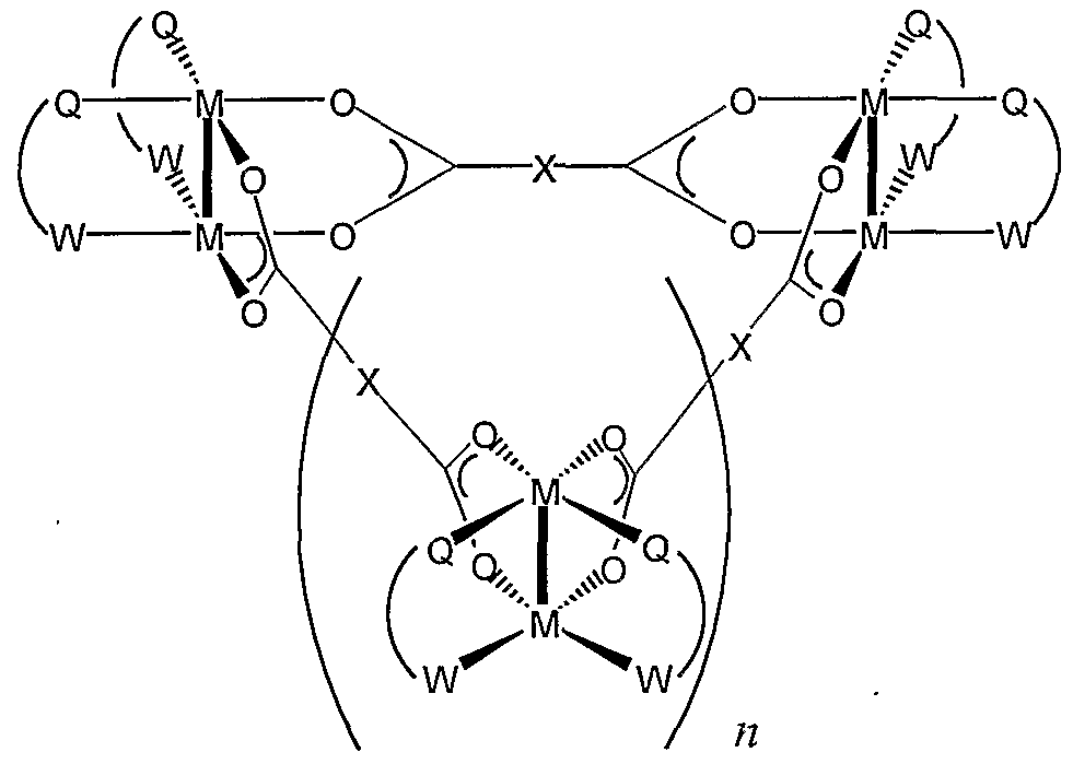
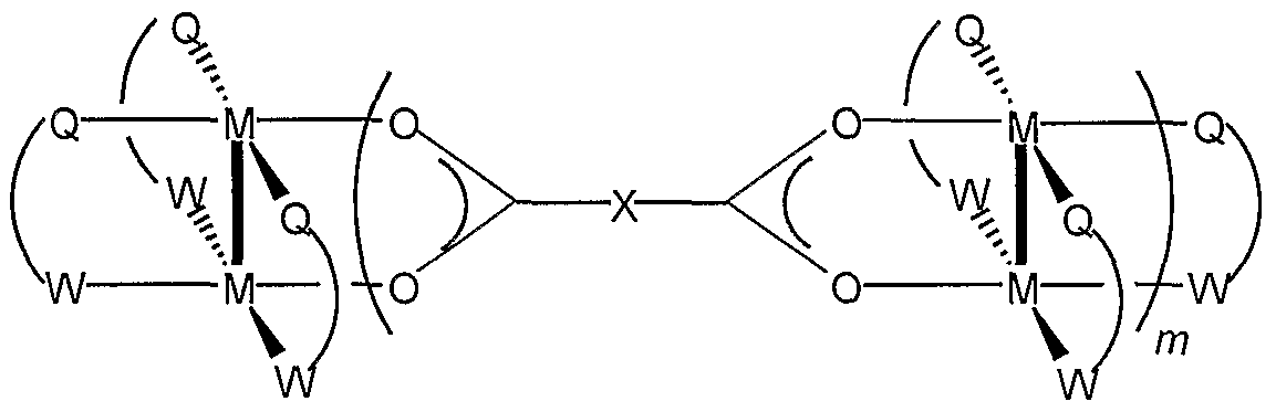
- L ax is an axial ligand
- L eq is an equatorial ligand; wherein two equatorial ligands together form a bidentate ligand Q '" ⁇ /V; wherein each Q ⁇ W is independently selected from the group consisting of: N"N, N"O, O ⁇ N, N""S, S ⁇ N, N ⁇ P, P N, O ⁇ S, S ⁇ O, O ⁇ O, P ⁇ P and S ⁇ S ligands;
- M is a transition metal
- o o is a bridging group each selected independently from the group consisting of: SO 2" , MoO 4 2" , WO 4 2" , ZnCI 2" and a dicarboxylate; and wherein m is an integer from 1 to 25, and n is 0 to 6;
- G3-Linker b -G4 wherein G3 and G4 are the same or different functional groups capable of interacting with a metal-metal bonded complex; and Linkerb is a single bond or a difunctional organic group bonded to G3 and G4; and (iii) a solvent; and
- the processes described herein include layer-by-layer growth of thin films having alternating monolayers of metal-metal bonded complexes and organic molecules. Such films have utility in solid-state applications.
- the films are prepared by repeated sequential depositions of metal- metal bonded units, e.g., dirhodium tetraformamidinate complexes, on a prefunctionalized substrate, followed by a proper organic linker, e.g., dipyridyl organic molecules, for the next deposition sequence.
- metal- metal bonded units e.g., dirhodium tetraformamidinate complexes
- organic linker e.g., dipyridyl organic molecules
- the deposition method is a self-assembling, tunable and stepwise process. Upon application onto a substrate, the complexes are adsorbed on the substrate. Thereafter, an organic monolayer is applied. Thus, repeating the steps, a stepwise layer by layer growth of the thin films can be achieved.
- the multi-layered thin films can be grown layer-by-layer to the desired thickness.
- the process includes the following steps:
- G1-Linker a -G2 to produce a primer layer of the first linker compound on the substrate, wherein G1 is a functional group capable of interacting with the surface of the substrate; G2 is a functional group capable of interacting with a metal- metal bonded complex; and Linker a is a difunctional organic group bonded to G1 and G2;
- the metal-metal bonded complex being selected from the group consisting of compounds represented by the following formulas:
- L ax is an axial ligand
- M is a transition metal
- o o is a bridging group each independently selected from the group consisting of: SO 4 2" , MoO 4 2" , W0 4 2" , ZnCI 2" and a dicarboxylate; and wherein m is an integer from 1 to 25, and n is 0 to 6;
- G3 and G4 are the same or different functional groups capable of interacting with a metal-metal bonded complex; and Linker b is a single bond or a difunctional organic group bonded to G3 and G4; and optionally
- the thin film has from 1 to 100 alternating monolayers of a metal-metal bonded complex monolayer and an organic monolayer. More preferably, the thin film has from 30 to 40 alternating monolayers of a metal-metal bonded complex monolayer and an organic monolayer.
- the films are deposited from liquid solutions and therefore they may be deposited on substrates having diverse topography and configuration.
- the following illustration describes the layer-by-layer growth methods used according to the present invention to fabricate metal-metal bonded compounds on a substrate.
- any suitable material can be used as a substrate.
- Suitable substrates include, for example, a metal, a metal oxide, a semiconductor, a metal alloy, a semiconductor alloy, a polymer, an organic solid, and a combination thereof.
- the form of the substrates can be a planar solid or a non-planar solid such as a stepped or curved surface.
- the following preferred substrates have been demonstrated: Au, ITO and Si0 2 .
- G1-Linker a -G2 groups are suitable molecular species that can form a self-assembled monolayer include organic molecular species having a functional group G1 capable of interaction with the surface of the substrate forming a coated surface.
- Examples of this group that can be designed into molecules for interacting with or binding to a particular substate surface with chemical specificity include one or more of the same or different functional groups, such as phosphine oxide, phosphite, phosphate, phosphazine, azide, hydrazine, sulfonic acid, sulfide, disulfide, aldehyde, ketone, silane, germane, arsine, nitrile, isocyanide, isocyanate, thiocyanate, isothiocyanate, amide, alcohol, selenol, nitro, boronic acid, ether, thioether, carbamate, thiocarbamate, dithiocarbamate, dithiocarboxylate, xanthate, thioxanthate, alkylthiophosphate, dialkyldithiophosphate or a combination thereof.
- functional groups such as phosphine oxide, phosphite, phosphate
- Functional group G2 on the tran direction of G1 is capable of interaction with the next layer metal-metal boned molecules.
- this group that can be designed into molecules for interacting with or binding to a particular metal-metal bonded molecule with chemical specificity include one or more of the same or different functional groups.
- G2 in the first linker compound can independently be: 4-pyridyl, 3- pyridyl, cyano, 4-cyanophenyl, 3-cyanophenyl, perfluoro-3-cyanophenyl and perfluoro-4-cyanopheny.
- G2a and G2b There are two types of these molecules, G2a and G2b.
- G2a is used for the axial direction linkage, such as nitrile, pyridyl, trimethylsilane compounds; and the G2b is used for the equatorial direction linkage, such as some bridging bidentate ligands with (N,N), (N,O), (O,O), (O,S), (P,P), (N,S), and (S,S) donor sets.
- bidentate ligands are amidinates that are a (N,N) donor set, acetamides that are a (N,O) set, carboxylates that are a (O,O) set, thiocarboxylates that are a (O,S) set, diphosphines that are a (P,P) set, mercaptopyrimidines that are a (N,S) set, and dithiocarboxylates that are a (S,S) set.
- L- ⁇ J are suitable molecules containing at least one metal- metal bonded unit.
- examples of these metal-metal bonded complexs can be containing one or more than one metal-metal bonded units of which axial direction can interact with or bind to G2a group, such as the molecules containing one or more than one of the following metal-metal bonded cores: Cr 2 4+ , Mo 2 4+ , Re 2 6+ , Re 2 5+ , Re 2 4+ , Ru 2 5+ , Ru 2 6+ , Rh 2 4+ .
- Preferred molecules suitable for use as the molecular species that can interact with or bind to G2a group include: tetrakis(carboxylato)dichromium, tetrakis(carboxylato)dimolybdenum, tetrakis(amidinato)dichlorodirhenium, tetrakis(amidinato)chloro- diruthenium, tetrakis(carboxylato)dirhodium, tetrakis(amidinato)dirhodium, bis(carboxylato)bis(amidinato)dirhodium, and complexes containing more than one dimetal units.
- examples of these metal-metal bonded complexes can be containing one or more than one metal-metal bonded units of which equatorial direction can interact with or bind to G2b group, such as the molecules containing one of the following metal-metal bonded cores: Cr 2 + , Mo 2 4+ , W 2 4+ , Re 2 6+ , Re 2 5+ , Re 2 4+ , Ru 2 4+ , Ru 2 5+ , Ru 2 6+ , Os 2 6+ , Rh 2 4+ .
- Preferred molecules suitable for use as the molecular species that can interact with or bind to G2b group include: tetrakis(carboxylato)dimetal (where the metal is the one of the above), decakis(acetonitrile)dimetal (where the metal is Mo, Re, and Rh).
- G3- inker 4 - G4 are suitable molecules bearing two functional groups at both ends. These functional groups will interact with or bind to the previous metal-metal bonded unit terminated surface. Both G3 and G4 functional groups are every similar to G2.
- G3 and G4 in the second linker compound can independently be 4-pyridyl, 3-pyridyl, cyano, 4-cyanophenyl, 3-cyanophenyl, perfluoro-3- cyanophenyl and perfluoro-4-cyanopheny.
- Linker b can be a single bond, an alkylene, an alkenediyl, an alkynediyl, a 1 ,4-arylene, an arene-1 ,3,5- triyl, a 1 ,2,3-triazine-2,4,6-triyl, 4,4',4", 4"'-(21H,23H-porphine-5,10,15,20- tetrayl) and zinc complex of 4,4',4", 4"'-(21 H,23H-porphine-5, 10,15,20- tetrayl) and a combination thereof.
- G3-LinkenrG4 groups include polynitriles, polypyridyls, ditrimethylsilanes, and organic molecules containing at least two of any of the following donor sets used as bridging bidentate ligands: (N,N), (N,O), (O,O), (O,S), (P,P), (N,S), and (S,S), such as, NTI, NT), OT1, NT, STI, NT, PTI, OT, ST), OT), PT and S" ⁇ S ligands.
- Some molecules with tetrahedral geometry may also be used as equatorial linkers, such as S0 2" , MoO 4 2" , WO 4 2 -, ZnCI 4 2" .
- Examples of the second linker compounds include compounds represented by the following formulas:
- Preferred molecules carrying at least two required functional groups include:
- the process of the present invention includes the steps of:
- G1 is selected from the group consisting of: CI 3 Si and SH
- G2 is selected from the group consisting of: 4-pyridyl and 4-cyanophenyl
- Linker a is selected from the group consisting of:C- ⁇ -C 8 alkylene, C ⁇ -C 3 alkenediyl, C Cs alkynediyl and 1 ,4-arylene;
- metal-metal bonded complex (2) applying onto the primer layer a metal-metal bonded complex to produce on the primer layer a metal-metal bonded complex monolayer; wherein the metal-metal bonded complex is selected from the group consisting of compounds represented by the following formulas:
- L ax is an axial ligand
- L eq is an equatorial ligand
- two equatorial ligands together form a bidentate ligand QTV
- each QTV is independently selected from the group consisting of: NT, NT), OTI, NT>, ST, NT, PTJ, OT, ST, OT, PT and ST ligands
- M is a transition metal
- group o o is a dicarboxylate bridging group selected from the group consisting of compounds represented by the formulas:
- n is 0 to 3;
- G3 and G4 are the same or different functional groups capable of interacting with a metal-metal bonded complex; and Linker b is a single bond or a difunctional organic group bonded to G3 and G4; and optionally
- the substrates used for film growth can be various kinds of metals, insulators, and semiconductors such as glass, quartz, aluminum, gold, platinum, gold/palladium alloy, silicon, thermally grown silicon dioxide on silicon, and indium-tin-oxide coated glass. Since the films are deposited from liquid solutions, they may be deposited on substrates having diverse topography and configuration.
- the form of the substrates can be a planar solid or a non-planar solid such as a stepped or curved surface.
- the second step of thin film deposition is to treat the modified substrate with an appropriate compound containing at least one metal- metal bonded unit from solution.
- Metal-metal bond units will interact with N atoms through their axial directions or with bidentate ligands through their equatorial directions. The opposite direction that has not been used to interact with the molecular template will be used as the site for the next step of the layer-by-layer thin film growth.
- the metal atoms used in the metal-metal bonded units may be any of the following: V, Nb, Cr, Mo, W, Tc, Re, Fe, Ru, Os, Co, Rh, Ir, Ni, Pd, Pt, Cu, Ag.
- pyridyl functionalized oxide substrates such as quartz, indium-tin-oxide (ITO), and silicon wafers that have a native or thermally grown silicon dioxide surface.
- Substrates were first silated by immersion in a toluene solution containing 1 mM 4-[2-(trichlorosilyl)]-ethylpyridine for 30 min. After rinsing with copious amounts of toluene and ethanol, the substrates were vacuum-dried. Metal-metal bonded molecular films were grown by first dipping the substrates into a 0.1 mM toluene solution of molecule 1 for 2 h at -15 °C and then in a 0.1 mM ether solution of 2 for 30 min at room temperature, with rinsing between steps.
- Figure 1 shows a cross-sectional view of a typical two-terminal lateral electronic device having a substrate 10.
- the device includes a metal-metal bonded complex material layer 4.
- Layer 4 is a metal-metal bonded complex and serves as the active switching medium between the electrodes 6 and 8 fabricated on substrate 10.
- Figure 2 shows a cross-sectional view of a typical three-terminal lateral electronic device 20 in the configuration of a transistor.
- the transistor 20 includes a metal-metal bonded material layer 22.
- Layer 22 is a metal-metal bonded complex and serves as the channel between source and drain electrodes 24 and 26.
- the conductance of the metal-metal bonded complex is modulated across an electrically insulating layer 28, such as a thin SiO 2 film, by a gate electrode 30, which may be a degenerately doped silicon layer, all of which are fabricated on substrate 32.
- Figure 3 shows a cross-sectional view of a typical two-terminal vertical electronic device 40.
- Device 40 includes a metal-metal bonded complex material layer 42.
- Layer 42 is a metal-metal bonded complex and serves as the active switching medium between electrodes 44 and 46 fabricated on substrate 48.
- electrode 44 is deposited on top of the metal-metal bonded layer.
- Figure 4 shows a cross-sectional view of a typical three-terminal veritcal electronic device 60 in the configuration of a transistor.
- the transistor 60 includes a metal-metal bonded material layer 62.
- Layer 62 is a metal-metal bonded complex and serves as the channel between source and drain electrodes 64 and 66.
- the conductance of the metal-metal bonded complex is modulated across an electrically insulating layer 68, such as a thin SiO 2 film, by a gate electrode 70, which may be a degenerately doped silicon layer, all of which are fabricated on substrate 72.
- electrode 64 is deposited on top of the metal-metal bonded layer.
- Figure 5 shows AFM images of metal-metal bonded complex assembled layer-by-layer from solution showing the complex spanning the distance between Au electrodes as the number of bilayers is increased from (a) 0 bilayers, (b) 7 bilayers, (c) 17 bilayers, and (d) 30 bilayers.
- the Au electrodes were deposited onto 40 nm thick SiO 2 on a degenerately doped silicon substrate.
- Figure 6 shows line-cuts of the AFM images shown in Figure 5.
- the metal-metal bonded complex spans the distance between electrodes, closing the separation between electrodes as the number of bilayers is increased from (a) 0 bilayers, (b) 7 bilayers, (c) 17 bilayers, and (d) 30 bilayers.
- the metal-metal bonded complex spans the distance between electrodes, either by assembling the complex layer-by-layer or by spin- coating a polycrystalline thin film in which the metal-metal bonded units and the organic ligands self-assemble, the electrodes are electrically connected.
- Figure 8 shows negative differential resistance in the l-V characteristics for a metal-metal bonded complex in which Rh-Rh is the metal-metal bonded unit and 1 ,2-bis(4-pyridyl)ethylene is the ligand.
- the compound was grown layer-by-layer from Au electrodes using mercaptan ethylpyridine as the linker.
- the device is fabricated in the lateral geometry with an 80 nm spacing between metal electrodes.
- Figure 9 shows an AFM image of the metal-metal bonded complex in which Rh-Rh is the metal-metal bonded unit and zinc 5,10,15,20-tetra(4- pyridyl)-21 H,23H-porphine is the ligand.
- the complex was deposited by spin-coating from a solution in chloroform to form a polycrystalline thin film with grain structure consistent with the underlying structural motif of the metal-metal bonded complex.
- Figure 10 shows negative differential resistance in the l-V characteristics for a metal-metal bonded complex in which Rh-Rh is the metal-metal bonded unit and zinc 5,10,15,20-tetra(4-pyridyl)-21 H,23H- porphine is the ligand.
- the complex was deposited by spin-coating from a solution in chloroform.
- Figure 11 shows an AFM image of the metal-metal bonded complex in which Rh-Rh is the metal-metal bonded unit and 1 ,2-bis(4- pyridyl)ethylene is the ligand.
- the complex was deposited by spin-coating from a solution in chloroform to form a polycrystalline thin film with grain structure consistent with the underlying structural motif of the metal-metal bonded complex.
- Figure 12 shows negative differential resistance in the l-V characteristics for a metal-metal bonded complex in which Rh-Rh is the metal-metal bonded unit and 1 ,2-bis(4-pyridyl)ethylene is the ligand.
- the complex was deposited by spin-coating from a solution in chloroform.
- the electronic properties of the metal-metal bonded complexes may be tailored through chemistry. There is a wide-range of metal-metal and organic ligands usable as the metal-metal bonded complex. Metal- metal bonded complexes may be designed by choosing the chemistry and structural motif of the complex. The flexibility in the chemistry may be used to tailor the electronic properties of the molecular devices.
Landscapes
- Engineering & Computer Science (AREA)
- Chemical & Material Sciences (AREA)
- Physics & Mathematics (AREA)
- Materials Engineering (AREA)
- Nanotechnology (AREA)
- Theoretical Computer Science (AREA)
- Spectroscopy & Molecular Physics (AREA)
- Inorganic Chemistry (AREA)
- Crystallography & Structural Chemistry (AREA)
- Mathematical Physics (AREA)
- General Physics & Mathematics (AREA)
- Software Systems (AREA)
- Molecular Biology (AREA)
- General Health & Medical Sciences (AREA)
- General Engineering & Computer Science (AREA)
- Life Sciences & Earth Sciences (AREA)
- Computing Systems (AREA)
- Health & Medical Sciences (AREA)
- High Energy & Nuclear Physics (AREA)
- Thin Film Transistor (AREA)
- Electrodes Of Semiconductors (AREA)
Abstract
Description


Claims


Priority Applications (7)
| Application Number | Priority Date | Filing Date | Title |
|---|---|---|---|
| JP2003585194A JP4283119B2 (en) | 2002-04-05 | 2003-03-27 | Molecular electronic devices using metal-metal bonded complexes |
| AT03721488T ATE520157T1 (en) | 2002-04-05 | 2003-03-27 | MOLECULAR ELECTRONIC DEVICE WITH METAL-METAL COMPLEXES |
| MXPA04009562A MXPA04009562A (en) | 2002-04-05 | 2003-03-27 | Molecular electronic device using metal-metal bonded complexes. |
| KR1020047014081A KR100745527B1 (en) | 2002-04-05 | 2003-03-27 | Molecular Electronic Devices Using Metal-Metal Bonded Complexes |
| EP03721488A EP1493194B1 (en) | 2002-04-05 | 2003-03-27 | Molecular electronic device using metal-metal bonded complexes |
| CN03807494XA CN1643708B (en) | 2002-04-05 | 2003-03-27 | Molecular electronic device using metal-metal bonded complexes |
| AU2003224798A AU2003224798A1 (en) | 2002-04-05 | 2003-03-27 | Molecular electronic device using metal-metal bonded complexes |
Applications Claiming Priority (2)
| Application Number | Priority Date | Filing Date | Title |
|---|---|---|---|
| US10/117,789 | 2002-04-05 | ||
| US10/117,789 US6646285B1 (en) | 2002-04-05 | 2002-04-05 | Molecular electronic device using metal-metal bonded complexes |
Publications (2)
| Publication Number | Publication Date |
|---|---|
| WO2003088372A2 true WO2003088372A2 (en) | 2003-10-23 |
| WO2003088372A3 WO2003088372A3 (en) | 2003-11-20 |
Family
ID=29248208
Family Applications (1)
| Application Number | Title | Priority Date | Filing Date |
|---|---|---|---|
| PCT/US2003/009566 Ceased WO2003088372A2 (en) | 2002-04-05 | 2003-03-27 | Molecular electronic device using metal-metal bonded complexes |
Country Status (10)
| Country | Link |
|---|---|
| US (1) | US6646285B1 (en) |
| EP (1) | EP1493194B1 (en) |
| JP (1) | JP4283119B2 (en) |
| KR (1) | KR100745527B1 (en) |
| CN (1) | CN1643708B (en) |
| AT (1) | ATE520157T1 (en) |
| AU (1) | AU2003224798A1 (en) |
| MX (1) | MXPA04009562A (en) |
| TW (1) | TWI229704B (en) |
| WO (1) | WO2003088372A2 (en) |
Cited By (1)
| Publication number | Priority date | Publication date | Assignee | Title |
|---|---|---|---|---|
| WO2004006353A3 (en) * | 2002-07-03 | 2004-08-05 | Univ Cambridge Tech | Organic-inorganic hybrid transistors |
Families Citing this family (15)
| Publication number | Priority date | Publication date | Assignee | Title |
|---|---|---|---|---|
| US7189433B2 (en) * | 2002-04-05 | 2007-03-13 | International Business Machines Corporation | Process for preparing a film having alternatively monolayers of a metal-metal bonded complex monolayer and an organic monolayer by layer-by layer growth |
| DE10228772A1 (en) * | 2002-06-27 | 2004-01-15 | Infineon Technologies Ag | Reduction of the contact resistance in organic field effect transistors with palladium contacts by using nitriles and isonitriles |
| US7285440B2 (en) * | 2002-11-25 | 2007-10-23 | International Business Machines Corporation | Organic underlayers that improve the performance of organic semiconductors |
| US7132678B2 (en) * | 2003-03-21 | 2006-11-07 | International Business Machines Corporation | Electronic device including a self-assembled monolayer, and a method of fabricating the same |
| US7166327B2 (en) * | 2003-03-21 | 2007-01-23 | International Business Machines Corporation | Method of preparing a conjugated molecular assembly |
| DE102004010954A1 (en) * | 2004-03-03 | 2005-10-06 | Novaled Gmbh | Use of a metal complex as an n-dopant for an organic semiconductive matrix material, organic semiconductor material and electronic component |
| KR101151159B1 (en) * | 2006-09-19 | 2012-06-01 | 삼성전자주식회사 | Organic thin film transistor comprising phosphate-based selfassembly monolayer and method for manufacturing the same |
| JP2008124164A (en) * | 2006-11-10 | 2008-05-29 | Sony Corp | Semiconductor device and manufacturing method thereof |
| JP2008124360A (en) * | 2006-11-15 | 2008-05-29 | Sony Corp | Functional molecular device, manufacturing method thereof, and functional molecular device |
| DE102007028236A1 (en) * | 2007-06-20 | 2009-01-02 | Siemens Ag | Semiconducting material and organic rectifier diode |
| CN101118607B (en) * | 2007-09-07 | 2013-05-08 | 中国科学院上海微系统与信息技术研究所 | Real time detecting single electron spinning state method |
| JP5213458B2 (en) | 2008-01-08 | 2013-06-19 | キヤノン株式会社 | Amorphous oxide and field effect transistor |
| FR2967923A1 (en) * | 2010-11-30 | 2012-06-01 | Corning Inc | ORGANO-METALLIC STRUCTURE USED IN PARTICULAR AS A CATALYST, AS WELL AS ITS MANUFACTURING PROCESS |
| KR102078435B1 (en) * | 2016-07-14 | 2020-02-17 | 주식회사 엘지화학 | Organic light emitting diode and manufacturing method of the same |
| CN114121810B (en) | 2020-08-27 | 2024-12-06 | 长鑫存储技术有限公司 | Semiconductor structure and method for manufacturing the same |
Family Cites Families (12)
| Publication number | Priority date | Publication date | Assignee | Title |
|---|---|---|---|---|
| US4939556A (en) * | 1986-07-10 | 1990-07-03 | Canon Kabushiki Kaisha | Conductor device |
| US5152805A (en) * | 1989-12-29 | 1992-10-06 | Gte Laboratories Incorporated | M-I-M' device and fabrication method |
| IL98753A0 (en) * | 1990-10-10 | 1992-07-15 | Yeda Res & Dev | Process for the production of composite organic-inorganic superlattices |
| EP0482920A3 (en) * | 1990-10-24 | 1993-01-07 | Kabushiki Kaisha Toshiba | Organic optical element |
| US5217792A (en) | 1991-10-17 | 1993-06-08 | At&T Bell Laboratories | Stable polar optically nonlinear multilayer films and devices using the same |
| WO1999003154A1 (en) * | 1997-07-11 | 1999-01-21 | University Of Southern California | Charge generators in heterolamellar multilayer thin films |
| US6314019B1 (en) | 1999-03-29 | 2001-11-06 | Hewlett-Packard Company | Molecular-wire crossbar interconnect (MWCI) for signal routing and communications |
| US6128214A (en) | 1999-03-29 | 2000-10-03 | Hewlett-Packard | Molecular wire crossbar memory |
| US6459095B1 (en) | 1999-03-29 | 2002-10-01 | Hewlett-Packard Company | Chemically synthesized and assembled electronics devices |
| US6198655B1 (en) | 1999-12-10 | 2001-03-06 | The Regents Of The University Of California | Electrically addressable volatile non-volatile molecular-based switching devices |
| EP1215199A1 (en) * | 2000-12-08 | 2002-06-19 | Sony International (Europe) GmbH | Linker molecules for selective metallisation of nucleic acids and their uses |
| US20020167003A1 (en) * | 2001-04-18 | 2002-11-14 | Campbell Ian H. | Chemical and biological sensor using organic self-assembled transitors |
-
2002
- 2002-04-05 US US10/117,789 patent/US6646285B1/en not_active Expired - Lifetime
-
2003
- 2003-03-27 WO PCT/US2003/009566 patent/WO2003088372A2/en not_active Ceased
- 2003-03-27 AU AU2003224798A patent/AU2003224798A1/en not_active Abandoned
- 2003-03-27 CN CN03807494XA patent/CN1643708B/en not_active Expired - Lifetime
- 2003-03-27 MX MXPA04009562A patent/MXPA04009562A/en active IP Right Grant
- 2003-03-27 EP EP03721488A patent/EP1493194B1/en not_active Expired - Lifetime
- 2003-03-27 JP JP2003585194A patent/JP4283119B2/en not_active Expired - Fee Related
- 2003-03-27 AT AT03721488T patent/ATE520157T1/en not_active IP Right Cessation
- 2003-03-27 KR KR1020047014081A patent/KR100745527B1/en not_active Expired - Fee Related
- 2003-04-02 TW TW092107511A patent/TWI229704B/en not_active IP Right Cessation
Cited By (1)
| Publication number | Priority date | Publication date | Assignee | Title |
|---|---|---|---|---|
| WO2004006353A3 (en) * | 2002-07-03 | 2004-08-05 | Univ Cambridge Tech | Organic-inorganic hybrid transistors |
Also Published As
| Publication number | Publication date |
|---|---|
| CN1643708B (en) | 2011-04-13 |
| JP4283119B2 (en) | 2009-06-24 |
| EP1493194B1 (en) | 2011-08-10 |
| US20030203168A1 (en) | 2003-10-30 |
| US6646285B1 (en) | 2003-11-11 |
| ATE520157T1 (en) | 2011-08-15 |
| TWI229704B (en) | 2005-03-21 |
| KR20040104497A (en) | 2004-12-10 |
| CN1643708A (en) | 2005-07-20 |
| WO2003088372A3 (en) | 2003-11-20 |
| AU2003224798A1 (en) | 2003-10-27 |
| KR100745527B1 (en) | 2007-08-03 |
| MXPA04009562A (en) | 2005-01-25 |
| TW200401844A (en) | 2004-02-01 |
| JP2006508525A (en) | 2006-03-09 |
| EP1493194A2 (en) | 2005-01-05 |
Similar Documents
| Publication | Publication Date | Title |
|---|---|---|
| EP1493194B1 (en) | Molecular electronic device using metal-metal bonded complexes | |
| US8021753B2 (en) | Film having alternating monolayers of a metal-metal bonded complex monolayer and an organic monolayer by layer-by-layer growth | |
| CN100377795C (en) | Conjugated molecular assemblies, methods of making the assemblies, and devices comprising the assemblies | |
| Ulman | Formation and structure of self-assembled monolayers | |
| Liedberg et al. | Self-assembly of α-functionalized terthiophenes on gold | |
| Maskus et al. | Synthesis and characterization of redox-active metal complexes sequentially self-assembled onto gold electrodes via a new thiol− terpyridine ligand | |
| Li et al. | Surface confined metallosupramolecular architectures: formation and scanning tunneling microscopy characterization | |
| Heimel et al. | The interface energetics of self-assembled monolayers on metals | |
| Steinem et al. | Valinomycin-mediated transport of alkali cations through solid supported membranes | |
| Rubio-Gimenez et al. | Ultrathin films of 2D Hofmann-type coordination polymers: influence of pillaring linkers on structural flexibility and vertical charge transport | |
| KR101202568B1 (en) | Method for Manufacturing Insulated Gate Field Effect Transistors | |
| Albers et al. | Design of novel molecular wires for realizing long-distance electron transfer | |
| Li et al. | Effect of Electric Fields on Silicon-Based Monolayers | |
| Taherinia | Investigation of the interfacial electron transfer kinetics in ferrocene-terminated oligophenyleneimine self-assembled monolayers | |
| KR100836759B1 (en) | Organic memory device and method of forming the same | |
| McCreery et al. | Surface functionalization in the nanoscale domain | |
| KR100661695B1 (en) | Semiconductor thin film using self-assembled monolayer and its manufacturing method | |
| JP2008249511A (en) | Humidity sensor | |
| RU2796048C1 (en) | Reservoir computing device based on organometallic framework polymer and method for its manufacture | |
| Gupta et al. | Self-assembled and electrochemically deposited mono/multilayers for molecular electronics applications | |
| KR100347763B1 (en) | The manufacturing method of multilayer thin film using spin coating | |
| Patil et al. | Self-assembled multilayer formation of an aromatic bifunctional molecule via selective ionic interaction | |
| Joo | New functionalized polyoxometalates (POMS) for molecular memory devices compatible with a CMOS processing | |
| KR20030007024A (en) | A manufacturing method for monolayer/multilayer ultrathin films using spin coating | |
| DES NOUVEAUX DERIVÉS | NICOLETA JOO |
Legal Events
| Date | Code | Title | Description |
|---|---|---|---|
| AK | Designated states |
Kind code of ref document: A2 Designated state(s): AE AG AL AM AT AU AZ BA BB BG BR BY BZ CA CH CN CO CR CU CZ DE DK DM DZ EC EE ES FI GB GD GE GH GM HR HU ID IL IN IS JP KE KG KP KR KZ LC LK LR LS LT LU LV MA MD MG MK MN MW MX MZ NO NZ OM PH PL PT RO RU SD SE SG SK SL TJ TM TN TR TT TZ UA UG UZ VN YU ZA ZM ZW |
|
| AL | Designated countries for regional patents |
Kind code of ref document: A2 Designated state(s): GH GM KE LS MW MZ SD SL SZ TZ UG ZM ZW AM AZ BY KG KZ MD RU TJ TM AT BE BG CH CY CZ DE DK EE ES FI FR GB GR HU IE IT LU MC NL PT RO SE SI SK TR BF BJ CF CG CI CM GA GN GQ GW ML MR NE SN TD TG |
|
| DFPE | Request for preliminary examination filed prior to expiration of 19th month from priority date (pct application filed before 20040101) | ||
| 121 | Ep: the epo has been informed by wipo that ep was designated in this application | ||
| WWE | Wipo information: entry into national phase |
Ref document number: 1020047014081 Country of ref document: KR |
|
| WWE | Wipo information: entry into national phase |
Ref document number: 2003807494X Country of ref document: CN |
|
| WWE | Wipo information: entry into national phase |
Ref document number: 2185/CHENP/2004 Country of ref document: IN |
|
| WWE | Wipo information: entry into national phase |
Ref document number: PA/a/2004/009562 Country of ref document: MX |
|
| WWE | Wipo information: entry into national phase |
Ref document number: 2003585194 Country of ref document: JP |
|
| WWE | Wipo information: entry into national phase |
Ref document number: 2003721488 Country of ref document: EP |
|
| WWP | Wipo information: published in national office |
Ref document number: 1020047014081 Country of ref document: KR |
|
| WWP | Wipo information: published in national office |
Ref document number: 2003721488 Country of ref document: EP |