WO2003098587A1 - Charge/discharge control circuit, light emitting device, and drive method thereof - Google Patents
Charge/discharge control circuit, light emitting device, and drive method thereof Download PDFInfo
- Publication number
- WO2003098587A1 WO2003098587A1 PCT/JP2003/006169 JP0306169W WO03098587A1 WO 2003098587 A1 WO2003098587 A1 WO 2003098587A1 JP 0306169 W JP0306169 W JP 0306169W WO 03098587 A1 WO03098587 A1 WO 03098587A1
- Authority
- WO
- WIPO (PCT)
- Prior art keywords
- light emitting
- charge
- charging
- path
- emitting device
- Prior art date
- Legal status (The legal status is an assumption and is not a legal conclusion. Google has not performed a legal analysis and makes no representation as to the accuracy of the status listed.)
- Ceased
Links
Classifications
-
- G—PHYSICS
- G09—EDUCATION; CRYPTOGRAPHY; DISPLAY; ADVERTISING; SEALS
- G09G—ARRANGEMENTS OR CIRCUITS FOR CONTROL OF INDICATING DEVICES USING STATIC MEANS TO PRESENT VARIABLE INFORMATION
- G09G3/00—Control arrangements or circuits, of interest only in connection with visual indicators other than cathode-ray tubes
- G09G3/20—Control arrangements or circuits, of interest only in connection with visual indicators other than cathode-ray tubes for presentation of an assembly of a number of characters, e.g. a page, by composing the assembly by combination of individual elements arranged in a matrix no fixed position being assigned to or needed to be assigned to the individual characters or partial characters
- G09G3/22—Control arrangements or circuits, of interest only in connection with visual indicators other than cathode-ray tubes for presentation of an assembly of a number of characters, e.g. a page, by composing the assembly by combination of individual elements arranged in a matrix no fixed position being assigned to or needed to be assigned to the individual characters or partial characters using controlled light sources
- G09G3/30—Control arrangements or circuits, of interest only in connection with visual indicators other than cathode-ray tubes for presentation of an assembly of a number of characters, e.g. a page, by composing the assembly by combination of individual elements arranged in a matrix no fixed position being assigned to or needed to be assigned to the individual characters or partial characters using controlled light sources using electroluminescent panels
- G09G3/32—Control arrangements or circuits, of interest only in connection with visual indicators other than cathode-ray tubes for presentation of an assembly of a number of characters, e.g. a page, by composing the assembly by combination of individual elements arranged in a matrix no fixed position being assigned to or needed to be assigned to the individual characters or partial characters using controlled light sources using electroluminescent panels semiconductive, e.g. using light-emitting diodes [LED]
- G09G3/3208—Control arrangements or circuits, of interest only in connection with visual indicators other than cathode-ray tubes for presentation of an assembly of a number of characters, e.g. a page, by composing the assembly by combination of individual elements arranged in a matrix no fixed position being assigned to or needed to be assigned to the individual characters or partial characters using controlled light sources using electroluminescent panels semiconductive, e.g. using light-emitting diodes [LED] organic, e.g. using organic light-emitting diodes [OLED]
- G09G3/3266—Details of drivers for scan electrodes
-
- G—PHYSICS
- G09—EDUCATION; CRYPTOGRAPHY; DISPLAY; ADVERTISING; SEALS
- G09G—ARRANGEMENTS OR CIRCUITS FOR CONTROL OF INDICATING DEVICES USING STATIC MEANS TO PRESENT VARIABLE INFORMATION
- G09G3/00—Control arrangements or circuits, of interest only in connection with visual indicators other than cathode-ray tubes
- G09G3/20—Control arrangements or circuits, of interest only in connection with visual indicators other than cathode-ray tubes for presentation of an assembly of a number of characters, e.g. a page, by composing the assembly by combination of individual elements arranged in a matrix no fixed position being assigned to or needed to be assigned to the individual characters or partial characters
- G09G3/22—Control arrangements or circuits, of interest only in connection with visual indicators other than cathode-ray tubes for presentation of an assembly of a number of characters, e.g. a page, by composing the assembly by combination of individual elements arranged in a matrix no fixed position being assigned to or needed to be assigned to the individual characters or partial characters using controlled light sources
- G09G3/30—Control arrangements or circuits, of interest only in connection with visual indicators other than cathode-ray tubes for presentation of an assembly of a number of characters, e.g. a page, by composing the assembly by combination of individual elements arranged in a matrix no fixed position being assigned to or needed to be assigned to the individual characters or partial characters using controlled light sources using electroluminescent panels
- G09G3/32—Control arrangements or circuits, of interest only in connection with visual indicators other than cathode-ray tubes for presentation of an assembly of a number of characters, e.g. a page, by composing the assembly by combination of individual elements arranged in a matrix no fixed position being assigned to or needed to be assigned to the individual characters or partial characters using controlled light sources using electroluminescent panels semiconductive, e.g. using light-emitting diodes [LED]
- G09G3/3208—Control arrangements or circuits, of interest only in connection with visual indicators other than cathode-ray tubes for presentation of an assembly of a number of characters, e.g. a page, by composing the assembly by combination of individual elements arranged in a matrix no fixed position being assigned to or needed to be assigned to the individual characters or partial characters using controlled light sources using electroluminescent panels semiconductive, e.g. using light-emitting diodes [LED] organic, e.g. using organic light-emitting diodes [OLED]
- G09G3/3216—Control arrangements or circuits, of interest only in connection with visual indicators other than cathode-ray tubes for presentation of an assembly of a number of characters, e.g. a page, by composing the assembly by combination of individual elements arranged in a matrix no fixed position being assigned to or needed to be assigned to the individual characters or partial characters using controlled light sources using electroluminescent panels semiconductive, e.g. using light-emitting diodes [LED] organic, e.g. using organic light-emitting diodes [OLED] using a passive matrix
-
- G—PHYSICS
- G09—EDUCATION; CRYPTOGRAPHY; DISPLAY; ADVERTISING; SEALS
- G09G—ARRANGEMENTS OR CIRCUITS FOR CONTROL OF INDICATING DEVICES USING STATIC MEANS TO PRESENT VARIABLE INFORMATION
- G09G3/00—Control arrangements or circuits, of interest only in connection with visual indicators other than cathode-ray tubes
- G09G3/20—Control arrangements or circuits, of interest only in connection with visual indicators other than cathode-ray tubes for presentation of an assembly of a number of characters, e.g. a page, by composing the assembly by combination of individual elements arranged in a matrix no fixed position being assigned to or needed to be assigned to the individual characters or partial characters
- G09G3/34—Control arrangements or circuits, of interest only in connection with visual indicators other than cathode-ray tubes for presentation of an assembly of a number of characters, e.g. a page, by composing the assembly by combination of individual elements arranged in a matrix no fixed position being assigned to or needed to be assigned to the individual characters or partial characters by control of light from an independent source
- G09G3/36—Control arrangements or circuits, of interest only in connection with visual indicators other than cathode-ray tubes for presentation of an assembly of a number of characters, e.g. a page, by composing the assembly by combination of individual elements arranged in a matrix no fixed position being assigned to or needed to be assigned to the individual characters or partial characters by control of light from an independent source using liquid crystals
-
- G—PHYSICS
- G09—EDUCATION; CRYPTOGRAPHY; DISPLAY; ADVERTISING; SEALS
- G09G—ARRANGEMENTS OR CIRCUITS FOR CONTROL OF INDICATING DEVICES USING STATIC MEANS TO PRESENT VARIABLE INFORMATION
- G09G2310/00—Command of the display device
- G09G2310/02—Addressing, scanning or driving the display screen or processing steps related thereto
- G09G2310/0243—Details of the generation of driving signals
- G09G2310/0251—Precharge or discharge of pixel before applying new pixel voltage
-
- G—PHYSICS
- G09—EDUCATION; CRYPTOGRAPHY; DISPLAY; ADVERTISING; SEALS
- G09G—ARRANGEMENTS OR CIRCUITS FOR CONTROL OF INDICATING DEVICES USING STATIC MEANS TO PRESENT VARIABLE INFORMATION
- G09G2310/00—Command of the display device
- G09G2310/02—Addressing, scanning or driving the display screen or processing steps related thereto
- G09G2310/0264—Details of driving circuits
- G09G2310/0275—Details of drivers for data electrodes, other than drivers for liquid crystal, plasma or OLED displays, not related to handling digital grey scale data or to communication of data to the pixels by means of a current
-
- G—PHYSICS
- G09—EDUCATION; CRYPTOGRAPHY; DISPLAY; ADVERTISING; SEALS
- G09G—ARRANGEMENTS OR CIRCUITS FOR CONTROL OF INDICATING DEVICES USING STATIC MEANS TO PRESENT VARIABLE INFORMATION
- G09G2320/00—Control of display operating conditions
- G09G2320/02—Improving the quality of display appearance
-
- G—PHYSICS
- G09—EDUCATION; CRYPTOGRAPHY; DISPLAY; ADVERTISING; SEALS
- G09G—ARRANGEMENTS OR CIRCUITS FOR CONTROL OF INDICATING DEVICES USING STATIC MEANS TO PRESENT VARIABLE INFORMATION
- G09G3/00—Control arrangements or circuits, of interest only in connection with visual indicators other than cathode-ray tubes
- G09G3/20—Control arrangements or circuits, of interest only in connection with visual indicators other than cathode-ray tubes for presentation of an assembly of a number of characters, e.g. a page, by composing the assembly by combination of individual elements arranged in a matrix no fixed position being assigned to or needed to be assigned to the individual characters or partial characters
- G09G3/22—Control arrangements or circuits, of interest only in connection with visual indicators other than cathode-ray tubes for presentation of an assembly of a number of characters, e.g. a page, by composing the assembly by combination of individual elements arranged in a matrix no fixed position being assigned to or needed to be assigned to the individual characters or partial characters using controlled light sources
Definitions
- the present invention relates to a charge / discharge control circuit for controlling charge / discharge in a light emitting device provided with a display unit in which a plurality of driven elements such as a plurality of light emitting elements and liquid crystal are arranged, a light emitting device, and a driving method thereof.
- LED displays are constructed by combining multiple LED units according to the installation location, and the LED units are composed of RGB light emitting diodes arranged in a dot matrix on a substrate. It is composed.
- the LED display is provided with a drive circuit that can individually drive each light emitting diode.
- each LED control device for transferring display data to each LED unit is connected, and a plurality of these are connected to form one large display.
- more LED units will be used. For larger ones, for example, a total of 120,000 LED units (300 x 400) will be used.
- the LED display a dynamic driving method is used as a driving method. Specifically, the LED display is connected and driven as follows.
- each light emitting diode (LED) located in each row is connected in common to one common source line, and each light emitting diode (LED) located in each column is connected.
- LED light emitting diode
- the display is performed by sequentially turning on the m-th common source line at a predetermined cycle.
- the switching of the m-th common source line is performed, for example, via a decoder circuit based on an address signal.
- the same drive circuit (method) can be driven in an electroluminescence display device, a field emission type display device (FED), a liquid crystal, and the like.
- FED field emission type display device
- a conventional display device such as an LED display device
- a light-emitting diode (light-emitting element) connected to a selected common source line is turned on, a non-selected non-lighted common source line is turned on.
- charges remain in the connected light emitting diode (light emitting element), and when the common source line is selected, extra current is generated due to the charges remaining when the common source line is not selected.
- the light emitting diode that is controlled not to emit light may emit a small amount of light, causing erroneous lighting or failing to provide sufficient contrast in the displayed image, resulting in poor display quality. It was the cause of lowering. Therefore, as shown in Fig. 3, a circuit 37 using only the resistor (R1) is provided in the drive circuit, and the circuit 37 remaining on the anode terminal side of the light-emitting diode connected to the unselected common source line A method of discharging electric charge from the ground terminal has been used.
- the present invention can reduce the influence of the above-described residual charges, and can realize a charge / discharge control circuit capable of realizing a light emitting device such as an LED display device, a liquid crystal display device, an EL display device, or a light receiving device such as a CCD having a high display quality. It is an object to provide an apparatus and a driving method thereof. Disclosure of the invention
- the invention according to claim 1 provides a driven element having a drive state and a non-drive state, a charging element having one end grounded, and a drive connected to the driven element to control the drive state and the non-drive state.
- a charge / discharge control circuit including a circuit, which charges a charge element in a non-drive state with a residual charge generated in a driven element and / or a wiring connected to the driven element, the charge being connected to the driven element.
- a charge / discharge control circuit having a charging path and a discharging path connected to the charging element and discharging the residual charge from the charging element to the ground terminal in a driving state.
- the driven element comprises a plurality of driven elements arranged in a matrix of m rows and n columns, and one terminal of each driven element arranged in each column is connected. Each is connected to a first line provided for each column, and the other terminal of each driven element arranged for each row is connected to a second line provided for each row. It is a charge / discharge control circuit that controls at least one of a first line and a second line.
- the invention according to claim 3 is a charge / discharge control circuit in which the charging path and the discharging path have one end grounded via a charging element.
- the charge path is a charge / discharge control circuit including a load.
- the discharge path is a charge / discharge control circuit including a rectifier.
- a charging path which is connected to a driven element and charges a charging element in a non-driving state with a residual charge generated in the driven element and / or a wiring connected to the driven element. Is a charge / discharge control circuit connected to the anode terminal side of the driven element.
- the invention according to claim 7 is a charge / discharge control circuit in which one end of the rectifier is connected to a charging element, and the other end is connected to a ground side.
- the invention according to claim 8 is a charge / discharge control circuit in which the driven element is a semiconductor element having a parasitic capacitance.
- the invention according to claim 9 is a charge / discharge control circuit in which the charging element is a capacitor.
- the invention according to claim 10 is the charge / discharge control circuit, wherein the load is a resistor.
- the invention according to claim 11 is a charge / discharge control circuit in which the rectifier is a diode.
- the driven element is a charge / discharge control circuit that is a semiconductor light emitting element.
- the invention according to claim 13 is a charge / discharge control circuit in which the driven element is a light emitting diode.
- the invention according to claim 14 is that the driven element is a light emitting element, and the charge / discharge control circuit is a charge / discharge control circuit constituting an erroneous lighting prevention circuit for preventing erroneous lighting of the light emitting element.
- the invention according to claim 15 is a charge / discharge control circuit in which a charge path and a discharge path are the same path, and residual charge charged in the charging element is discharged as a driving current in a driving state of the driven element. .
- the invention according to claim 16 is a driven element having a driving state and a non-driving state, a charging element having one end grounded, and a driving circuit connected to the driven element to control the driving state and the non-driving state.
- a light-emitting device comprising: a charging path that is connected to the driven element and that charges the charging element in a non-driving state with residual charges generated in the driven element and / or wiring connected to the driven element.
- a light emitting device connected to the charging element and having a discharge path for discharging the residual charge from the charging element to the ground terminal in a driving state.
- the invention according to claim 17 is characterized in that the driven element comprises a plurality of driven elements arranged in a matrix of m rows and n columns, and one terminal of each driven element arranged in each column. Are connected to the first line provided for each column, and the other terminal of each driven element provided for each row is connected to the second line provided for each row.
- the light emitting device controls at least one of the first line and the second line.
- the invention according to claim 18 is a light-emitting device in which the charging path and the discharging path are grounded at one end via a charging element.
- the invention according to claim 19 is the light emitting device, wherein the charging path includes a load.
- the invention according to claim 20 is the light emitting device, wherein the discharge path includes a rectifier.
- the invention according to claim 21 is a charging device that charges a charging element in a non-driving state with a residual charge generated in a wiring connected to the driven element and connected to the driven element and / or the driven element.
- the path is a light emitting device connected to the anode terminal side of the driven element.
- the invention according to claim 22 is the light-emitting device, wherein one end of the rectifier is connected to the charging element, and the other end is connected to the ground.
- the invention according to claim 23 is the light emitting device, wherein the driven element is a semiconductor element having a parasitic capacitance.
- the invention according to claim 24 is the light emitting device, wherein the charging element is a capacitor.
- the invention according to claim 25 is the light-emitting device, wherein the load is a resistor.
- the invention according to claim 26 is the light-emitting device, wherein the rectifier is a diode.
- An invention according to claim 27 is the light emitting device, wherein the driven element is a semiconductor light emitting element.
- An invention according to claim 28 is the light-emitting device, wherein the driven element is a light-emitting diode.
- the invention according to claim 29 is the light-emitting device, wherein the driven element is a light-emitting device, and the light-emitting device constitutes a false lighting prevention circuit for preventing false lighting of the light-emitting device.
- the invention according to claim 30 is the light-emitting device, wherein the charging path and the discharging path are the same path, and the residual charge charged in the charging element is discharged as a driving current in a driving state of the driven element.
- a light emitting device comprises a plurality of light emitting elements arranged in a matrix of m rows and n columns, and each light emitting element arranged in each column.
- the driving state and the non-driving state are controlled by a plurality of light emitting elements connected to the current line, and an input lighting control signal.
- a drive circuit for controlling the conduction of each of the common source lines based on display data, wherein the drive circuit is connected to an anode terminal of each of the light emitting elements and the drive circuit.
- the anode terminal of the light emitting element when al the transition to a non-driven state And a discharge path connected to the charge path and discharging the residual charge from the charging element to the ground terminal in the driving state.
- a light emitting device comprising a false lighting prevention circuit.
- the light emitting device wherein the discharge path is a path that is connected to the charge path and reaches the ground terminal via the drive circuit. It is.
- the driving circuit further includes m switching circuits connected to the common source lines, respectively, and is input in the driving state.
- a current source switching circuit that connects a common source line specified by an address signal to a current source; and a storage circuit that stores n pieces of gradation data of the display data that are sequentially input.
- a constant current control circuit unit that turns on a current line corresponding to a gradation width corresponding to gradation data stored in the storage circuit.
- the charging path is a path including a charging element having one end connected to the anode terminal side of each of the light emitting elements and the other end grounded.
- the discharge path is a path including a rectifier having an anode terminal connected to the charging path and a cathode terminal connected to the ground end. 35.
- a light-emitting device according to any one of items 34 to 34.
- the discharge path including the rectifier By forming the discharge path including the rectifier in this way, the residual charges can be reliably discharged, and the effect of the residual charges is substantially eliminated, so that a light emitting device with high display quality can be easily provided. be able to.
- the invention according to claim 36 according to the present invention is the light emitting device according to claims 31 to 35, wherein the charging path is a path including at least one resistor.
- the invention according to claim 37 of the present invention is the light emitting device according to any one of claims 31 to 36, wherein the light emitting element is a light emitting diode.
- the invention according to claim 38 of the present invention is the light emitting device according to claims 31 to 37, wherein the charging element is a capacitor.
- the invention according to claim 39 according to the present invention is the light emitting device according to claims 31 to 38, wherein the rectifier is a diode.
- the invention according to claim 40 according to the present invention is the light emitting device according to claims 31 to 39, wherein the light emitting device is an LED display.
- a plurality of light-emitting elements are arranged in a matrix of m rows and n columns, and the cathode terminals of each light-emitting element arranged in each column are respectively
- a display unit connected to a current line provided for each column and an anode terminal of each light emitting element arranged for each row connected to a common source line provided for each row, and connected to the current line;
- the driving state and the non-driving state are controlled by the plurality of light emitting elements thus input and the input lighting control signal, and the energization of each of the common source lines is controlled based on the display data input in each driving state.
- a driving method of a light emitting device having a driving circuit comprising: controlling a driving state and a non-driving state by a lighting control signal for controlling a lighting state and a non-lighting state; Controlling the energization of one end of each of the common source lines and one end of each of the current lines based on the display data to be displayed, and the charging path connected to the anode terminal of each of the light emitting elements and the driving circuit.
- a control circuit, a light-emitting device, and a driving method thereof can be provided.
- a control circuit, a light-emitting device, and a driving method thereof can be provided.
- the above-described residual charges can be reliably discharged, and by substantially eliminating the influence of the residual charges, charge / discharge control capable of realizing a display device with high display quality can be realized.
- a circuit, a light-emitting device, and a driving method thereof can be provided.
- the present invention can be used as a charge / discharge control circuit, a light emitting device, and a driving method thereof capable of realizing a display device with high display quality.
- the driving state can be set by flowing a desired current, and if the driven element is a voltage driving element, a desired voltage can be applied. It can be in a driving state.
- the current / voltage application state in the above-mentioned driving and non-driving states can be reversed, and various current / voltage application states can be set depending on the characteristics of the driven element.
- a driving state and a non-driving state exist for an element that is controlled by, for example, an electric field or a magnetic field other than the current and the voltage.
- the driving state and the non-driving state as referred to herein refer to at least two or more different states that can be recognized or observed and evaluated.
- the driving level in the driving state and the non-driving level in the non-driving state Each of two or more stages 6169
- a driven element refers to an element or a device that is driven based on a drive control signal or the like.
- it is an element with a capacitance component, such as a semiconductor light emitting diode—liquid crystal, EL, laser diode, CCD, photodiode, phototransistor, semiconductor memory, CPU, various sensors, various electronic devices, Conductive elements, rectifiers such as diodes and thyristors, light-emitting elements, light-receiving elements, etc., but have some kind of capacitance, including parasitic capacitance, such as diodes, bipolar, FETs, HEMTs, and other transistors, capacitors, etc.
- parasitic capacitance such as diodes, bipolar, FETs, HEMTs, and other transistors, capacitors, etc.
- driven element does not necessarily mean only a single element, but a device having a plurality of elements, for example, one pixel or a group of pixels that drives a plurality of LEDs as one pixel, a semiconductor laser diode, or the like.
- An array such as an array or an array group may be used, and in this sense, a unit to be driven.
- the charging element is typically a capacitor, but any element or device capable of temporarily storing and holding electric charge regardless of the amount and releasing the stored and held electric charge at a predetermined time. Any type can be used as the charging element according to the present specification. In addition, it is not always necessary to release all the charges temporarily stored and held in the charging element. Furthermore, the residual charge to be charged is the charge remaining on the driven element, its periphery, connected wiring, and the like, but a part of the residual charge is charged even if not all of it is charged. It may be good to keep it. Grounding one end typically means electrically connecting the charging element so that the potential at one end of the charging element is substantially at the ground potential.
- the specific configuration of the circuit does not matter as long as it is electrically connected.
- the circuit does not need to be grounded at all times, and can be grounded as appropriate according to the circuit drive (for example, a 5 V specified by a switch circuit). It is also possible to use a circuit capable of switching between the potential and the land access.
- an electric element or the like is appropriately provided between one end of the charging element and the ground, and a bias is applied to one end of the charging element to the extent that the charging / discharging control drive to the charging element described in this specification can be performed. Even in a certain state, there is no problem in practicing the present invention.
- connection typically means electrically connecting, and does not necessarily mean only physical connection.
- electro-optical devices such as EIC (Sub-Electronic Integrated Circuit)
- EIC Electro-Electronic Integrated Circuit
- electromagnetic fields such as electricity and light, pressure, sound waves, and radio waves
- connection the state of 'connected' so that transmission and reception of signals and transmission and reception of various kinds of energy using heat or the like as a medium
- direct connection the state of 'connected' so that transmission and reception of signals and transmission and reception of various kinds of energy using heat or the like as a medium
- direct connection does not matter.
- the residual charge is typically generated in a charge element that has a parasitic capacitance component, but even in a driven element that does not have a parasitic capacitance component, it floats on the wiring or the like connected to the element or in the vicinity. It exists and occurs in the form of capacity. Such residual charges tend to increase as the wiring length increases and the number of wires increases, and therefore, erroneous lighting, erroneous driving, erroneous display, and erroneous operation due to these residual charges also increase. In the present invention, it is possible to remove the residual charge generated in the connection wiring to the driven element, and the above problem can be solved.
- the optimal residual charge amount at the start of driving differs depending on the drive initial operating voltage and drive initial operating current that are optimal for the operation of the driven element.
- the residual charge can be removed until the desired amount of charge optimal for the above-mentioned operation drive is achieved, and malfunction, malfunction, light emission, etc. can be reduced to a level where there is no practical problem. It is sufficient if the residual charge can be removed to a certain extent, and it is not necessary to remove all the residual charge. As a typical example, in the case of the light emitting diode described in the embodiment shown in FIG. Is desirable.
- the amount of residual charge that can be removed can be designed and adjusted by appropriately adjusting a desired load, a charging element, a rectifier, and the like.
- the residual charge referred to in this specification can correspond to both positive and negative residual charges in relation to the driven element, and the residual charge can be appropriately set by setting the bias of the charge / discharge control circuit. It is possible not only to remove the charge but also to configure so that the charge opposite to that during driving remains.
- the driven element is composed of a rectifying element having a rectifying action (typically a diode and furthermore a light emitting diode)
- the charge / discharge control circuit of the present invention provides a reverse bias between the time when the driven element is driven and the time when the driven element is driven.
- the charging path is a path for accumulating charge in the charging element. It is only necessary to be connected so that some or all of the charge can move from the driven element and its surroundings, the wiring connected to the driven element to the charging element, and it is short-circuited so that current always flows. It does not have to be in the state. It is desirable that the charging path has a configuration that has a small resistance to the resistance of the driven element during charging so that the electric charge of the driven element can easily move to the charging element, and has a resistance of about 1 k ⁇ . It is more preferable to configure as follows.
- the ground terminal means a terminal electrically connected to the ground. It does not matter whether the length of the wiring up to the ground or the device between them, that is, direct ground or indirect ground.
- a discharge path is a path for discharging electric charge from a charging element. It is sufficient if some or all of the charge stored in the charging element can be moved from the charging element to the ground or a desired discharge point, and it is short-circuited so that current always flows. It does not have to be.
- a configuration including a switch circuit such as a transistor for controlling the timing of discharge and a rectifier may be employed.
- Discharge destination In addition to the ground discharge to the ground, it is also possible to make the discharge to be used as part or all of the drive current to the driven element.In this case, it is possible to drive effectively without discarding the residual charge Since it can be reused as electric current, energy saving and an eco-recycling circuit can be realized.
- a charge / discharge control circuit is a circuit provided to remove, reduce, or appropriately control residual charge generated in a driven element, its periphery, and wiring connected to the driven element.
- it has a drive circuit for controlling the driving and non-driving of the driven element, and has a charging element and a charging path and a discharging path for charging the charging element.
- the charging element is a capacitor, and preferably includes a resistor and a rectifier.
- a transistor, a switch circuit, or the like can be provided as appropriate in order to control charging and discharging.
- m and n are each an integer of 0 or more.
- a dot line-shaped array of only one row or one column may be used, and an array composed of one row and one column, that is, only one driven element may be included.
- the matrix is as described above, and is not a word that expresses the overall shape.It is not always necessary to form a square mesh, so even an arrangement that allows a flexible and flexible shape change is possible. Good thing.
- the actual shape and form are not limited as long as the connected connection form is a matrix connection. However, it is more preferable to use a matrix including the actual shape, because the wiring of the charge / discharge control circuit can be simplified.
- the first line can be a common line, a current drive line, a voltage drive line, a common source line, or the like.
- the second line can be a common line, a current drive line, a voltage drive line, a common source line, or the like.
- a semiconductor element having a parasitic capacitance is typically a light-emitting diode, a transistor, a photodiode, a phototransistor, a CCD, a memory, a liquid crystal, a light-emitting device such as an EL (electret luminescence) device, a light-receiving device, or a display device. It is a control element.
- a parasitic capacitance not only a semiconductor device but also a semiconductor device including a plurality of semiconductor devices or a semiconductor device including a semiconductor device and a peripheral circuit (typically, an IC or the like) are described in this specification.
- Semiconductor element In other words, the term “element” as used herein means not only a single device but also one unit, and is used to mean one unit of a semiconductor device group.
- the same charge path and discharge path typically means that they are the same electrical path, and both paths have opposite current directions.
- An electronic functional element such as a transistor can be provided in both paths. In this case, it is not always necessary that the current path inside the electronic functional element such as a transistor is the same.
- FIG. 1 is a conceptual diagram conceptually showing a configuration of a display device according to an embodiment of the present invention.
- FIG. 2 is a circuit diagram showing a specific example of the false lighting prevention circuit according to the present invention.
- FIG. 3 is a circuit diagram shown for comparison with a false lighting prevention circuit according to the present invention.
- FIG. 4 is a diagram showing experimental results for comparison with the false lighting prevention circuit according to the present invention.
- FIG. 5 is a diagram showing an experimental result for confirming the effectiveness of the false lighting prevention circuit according to the present invention.
- FIG. 6 is a timing chart when controlling the display device according to the present invention.
- FIG. 7 is an explanatory diagram of the first step of the second driving method of the present invention.
- FIG. 8 is an explanatory diagram of a second step of the second driving method according to the present invention.
- FIG. 9 is an explanatory diagram of the third step of the second driving method according to the present invention.
- FIG. 10 is an explanatory diagram of a fourth step of the second driving method according to the present invention.
- FIG. 11 is an explanatory diagram according to the embodiment of the present invention.
- FIG. 12 is an explanatory diagram relating to a third embodiment of the pseudo lighting prevention circuit.
- FIG. 13 is an explanatory diagram relating to a fourth embodiment of the pseudo lighting prevention circuit.
- FIG. 14 is an explanatory diagram relating to a fifth embodiment of the pseudo lighting prevention circuit.
- FIG. 15 is an explanatory diagram relating to a sixth embodiment of the pseudo lighting prevention circuit.
- FIG. 16 is an explanatory diagram related to Embodiment 7 of the pseudo lighting prevention circuit.
- FIG. 17 is an explanatory diagram related to Embodiment 8 of the false lighting prevention circuit.
- FIG. 1 is a conceptual diagram schematically showing a configuration of a light emitting device according to an embodiment of the present invention. As shown in the conceptual diagram of FIG.
- the plurality of light emitting elements 4 are arranged in a matrix of m rows and n columns, the cathode terminals of the light emitting elements 4 in each column are connected to the current lines 6, respectively, and the anode terminals of the light emitting elements 4 in each row are connected.
- a display unit configured by being connected to the common source line 5;
- a storage circuit is provided for storing each of the sequentially input n gradation data, and according to the gradation data stored in each storage circuit during the lighting period specified by the inputted lighting control signal.
- a constant current control circuit section 3 for driving a corresponding current line with a varied gradation width, and
- the current source switching circuit 1 includes a driving circuit for the common source driver 12 for controlling ON / OFF of the common source line, and a charging circuit connected to the anode terminal of each light emitting element and one end of the driving circuit.
- An erroneous lighting prevention circuit having a path and a discharge path connected to the charging path and reaching the ground terminal via the driving circuit.
- the charging path is a path through which the residual charge near each light emitting element flows into the charging element when the common source line is in a non-conductive state
- the discharging path is a common source line. This is a path through which the charge charged in the charging element is discharged at the ground terminal when the line is in a conductive state.
- the switching between the current source switching circuit 1 and the constant current control circuit unit 3 is performed by a lighting control signal, and when the lighting control signal indicates the lighting period, the current is switched.
- the source switching circuit 1 and the constant current control circuit 3 are driven.
- the common source line specified by the address signal input in the current source switching circuit 1 is connected to the current source, and the gradation stored in each memory circuit is stored in the constant current control circuit unit 3.
- each light emitting element connected to the common source line specified by the address signal is set to the corresponding grayscale level. Lights with the gradation width according to the data.
- the current source switching circuit 1 is not driven.
- the lighting control signal indicates a non-lighting period
- the charge remaining in each light emitting element or its surroundings is charged to the charging element through the charging path, and the lighting control signal sets the lighting period.
- the electric charge charged in the charging element is discharged from the ground terminal through the discharge path, so that almost no electric charge remains in each light emitting element or its periphery.
- the lighting period and the non-lighting period are sequentially repeated.
- the arranged light emitting elements are turned on.
- the electric charge accumulated in the light emitting element or its surroundings during the lighting period is discharged in the next non-lighting period, so that it is always unnecessary for each light emitting element and its surroundings during the lighting period.
- Lighting control can be performed in a state where no large charges are accumulated.
- the lighting can be controlled without being affected by the residual charge, so that a sufficient contrast can be obtained in a light emitting state, and a high quality display can be achieved.
- the current source switching circuit 1 is composed of a decoder circuit 11 and a common source driver 12, and the decoder circuit 11 is designated according to the address signal when the lighting control signal is at the LOW level. ONZOFF control of common source driver 12 so that common source line 5 and current source are connected.
- a field effect transistor FET
- the drive circuit can be provided in the common source driver 12. Here, one end of the switching element is grounded, and the other end is connected to the gate terminal of the FET via a resistor.
- the drain terminal of the FET is connected to the power supply, and the source terminal is connected to the anode terminal of each light emitting element.
- a charging path is formed by connecting the source terminal side of the FET or the anode terminal side of each light emitting element to the charging element via a resistor, and one end of the charging element is grounded. ing.
- one end of the charging element that is not grounded is connected to the gate terminal side of the FET via a rectifier to form a discharging path.
- the decoder circuit 11 controls the common source driver 12 so as to disconnect all the common source lines from the current source.
- the current source switching circuit 1 configured as described above, only the common source line 5 specified by the address signal when the lighting control signal is at the LOW level is supplied to the common source line 5 of the LED display section 10.
- the constant current control circuit unit 3 includes a shift register 31, a storage circuit 32, a counter 33, a data comparator 34, and a constant current driving unit 35.
- the constant current control circuit section 3 configured as described above shifts the grayscale data n times by the shift register 31 in synchronization with the shift clock, and responds to the latch clock to each of the n current lines. Is input to the storage circuit 32 and stored therein. Then, while the lighting control signal is at the low level, the value counted by the counter 33 is compared with the gradation data by the comparator 34 using the gradation reference clock as a counting clock. The current is input to the constant current drive unit 35, and the constant current drive unit 35 controls the constant current to flow through each current line during the drive pulse width corresponding to the gradation data value.
- the LED display gradation control is performed by the current source switching circuit 1 and the constant current control circuit unit 3 while the lighting control signal is at the low level. Note that while the lighting control signal is at the HIGH level, the LED display section 10 is not connected to the current source switching circuit 1 and the constant current control circuit section 3.
- the lighting control signal when the lighting control signal is at the L ⁇ W level, a predetermined light emitting diode is lit by driving the LED display unit 10 at a constant current, and the lighting control signal When is at the high level, the constant current drive of the LED display 10 is stopped.
- an LED display device using a light emitting diode as a light emitting element has been described.
- the present invention is not limited to this.
- the present invention can be similarly applied to a display device using another light emitting element such as a luminescence display device and a field emission type display device (FED).
- FED field emission type display device
- FIG. 1 is a conceptual diagram schematically illustrating the configuration of an LED display device according to an embodiment of the present invention. It is. Here, the false lighting prevention circuit 36 according to the present invention is provided for each common source line.
- a plurality of light emitting diodes 4 are arranged in a matrix of m rows and n columns, the cathode terminals of the light emitting diodes 4 in each column are connected to the current lines 6, respectively, and the light emitting diodes 4 in each row are connected.
- LED display section composed of ground terminals connected to common source line 5, respectively.
- m switch circuits connected to the common source line 5 respectively.
- the common source line specified by the address signal is connected to the current source during the lighting period specified by the input lighting control signal.
- a current source switching circuit 1 for supplying a current to the light emitting diode 4 connected to the common source line, and a storage circuit for storing sequentially inputted n pieces of gradation data.
- a constant current control circuit section 3 for driving a current line corresponding to a gradation width corresponding to the gradation data stored in each storage circuit in a lighting period specified by the control signal.
- FIG. 2 is a circuit diagram of a common source driver drive circuit and a false light prevention circuit 36 according to the present embodiment.
- the portion of the false lighting prevention circuit 36 in the present invention is a range surrounded by a broken line in FIG.
- a FET, a transistor for controlling 0 N / ⁇ FF of the FET, and a drive circuit including a plurality of resistors can be provided in the common source driver 12 for each common source line.
- An erroneous lighting prevention circuit 36 is provided for each of the drive circuits.
- an FET hereinafter referred to as “Q 1” or “Q 2”
- a transistor for controlling ON / OFF of the FET hereinafter referred to as “Q 3”
- a drive circuit including a plurality of resistors, and an erroneous lighting prevention circuit 36 are connected to an arbitrary common source line (hereinafter referred to as “common source line 1”) and another common source line (hereinafter referred to as “common source line 2”). This is described below.
- the emitter terminal of Q3 is grounded, the collector terminal is connected to the gate terminal of Q1 via resistor R3 (resistance 22 ⁇ ), and the base terminal is the decoder Connected to the circuit.
- the drain terminal of Q1 is connected to the power supply (5 V), and the number of source terminals is n for common source line 1. It is connected to the anode terminal of an arbitrary light emitting diode (hereinafter, referred to as “L lj”) among the light emitting diodes provided.
- a charge path is formed by connecting the anode terminal side to one end of a capacitor (hereinafter referred to as “C 1”) through a resistor R 1, and the other end of C 1 is grounded.
- one end of C1 which is not grounded, is connected to the gate terminal of Q1 and the collector terminal of Q3 via a diode (hereinafter referred to as "D1"), so that the end of the charging path is not connected.
- D1 diode
- the resistor R 1 installed in the middle of the charging path prevents a certain amount of charge from flowing into C 1 when the common source line 1 is selected and is in an energized state. The resistance is adjusted to prevent malfunction such as oscillation of Q1 due to an increase in gate voltage.
- the resistance value of R 1 is too small, the current that is discarded when driving the light emitting diode L 1 increases (Q 1 ⁇ R 1 ⁇ D 1 ⁇ Q 3 ⁇ ground earth), which does not contribute to lighting. Since current is generated, power consumption is increased and energy efficiency of the light emitting device is deteriorated, which is not preferable.
- the resistance value of R 1 is too large (up to 21 ⁇ or more), the residual charge of the light emitting diode L 1 becomes a resistance when charging the capacitor C 1, and the charge tends to be inhibited, which is not preferable.
- the optimum value can be determined by the resistance value of the light emitting diode before forward conduction, etc., but it has been found that an operation of around 1 ⁇ is very favorable (false lighting can be prevented).
- the diode D 1 installed in the middle of the discharge path is connected to the power supply (5 V) when Q 1 shifts from the driving state to the non-driving state, that is, when Q 3 changes to the non-driving state. Provided to prevent current from flowing into C1 through R2.
- the drive circuit for controlling the energization of the common source line 2 a drive circuit similar to that provided for the common source line 1 and a false lighting prevention circuit 36 are provided.
- the source terminal of Q 2 is connected to the anode terminal of an arbitrary light emitting diode (hereinafter referred to as “L 2”) among ⁇ light emitting diodes provided for the common source line 2.
- L 2 an arbitrary light emitting diode
- both L.1 and L2 are connected to one end of a driver IC in the constant current control circuit section 3, and the other end of the driver IC is grounded.
- the capacitance of C1 When determining the optimum value of the charge / discharge capacitor C1, the capacitance of C1 must be large. If it is too long, the residual charge of the light emitting diode L1 will easily charge the capacitor C1 and the amount of residual charge that can be accumulated will increase. However, when there is a reverse leakage current of the light emitting diode L1, Q2 ⁇ L2 ⁇ L1— It is not preferable because a large current path of R1 ⁇ C1 is generated, and the tendency of the light emitting diode L2 to erroneously light is increased. On the other hand, if the capacity of the charging and discharging capacitor C1 is too small, the residual charge generated in the light emitting diode L1 cannot be sufficiently stored in the capacitor C1.
- the light emitting diode L1 may be erroneously turned on due to the residual charge remaining.
- the capacitance of the capacitor C1 is about 0.01 F, which is the optimum value from the above viewpoint.
- FIG. 6 shows a timing chart when lighting control of the LED display device is performed using the false lighting prevention circuit of the present invention.
- a method of controlling the lighting of each common source line without accumulating the residual charge around L1 will be described step by step.
- Q 1 is a P-channel FET, a device that is energized when the potential of the gate terminal is LOW (0 V), and de-energized when the potential of the gate terminal is HIGH (5 V). It is.
- the common source line 1 is selected, that is, when Q 1 is energized, the gate potential of Q 1 is L OW, so the charge of C 1 (capacitance 0.01 / F) passes through the discharge path including D 1 Discharge from the emitter terminal side of the grounded Q3.
- FIG. 5 (c) shows the change with time of the anode terminal side voltage of L1 when no false lighting prevention circuit exists
- Fig. 5 (d) shows the results when the false lighting prevention circuit according to the present invention is used.
- FIG. 6 is a diagram showing a change with time of the anode terminal side voltage of L1. If there is no false lighting prevention circuit, as shown in Fig. 5 (c), at the moment Q1 is de-energized, the residual charge passes through L1, so the anode terminal voltage of L1 is Q1 Gradually decrease to the voltage level immediately before the driving state.
- the erroneous lighting prevention circuit according to the present invention when used, the residual charge is immediately charged to the capacitor at the moment when Q1 is turned off as shown in FIG.
- the node terminal voltage instantaneously drops to the voltage level immediately before Q1 enters the driving state.
- Q1 Indicates that almost no current is generated on the anode terminal side of L1 when the power is turned off. Therefore, it was confirmed that the erroneous lighting prevention circuit according to the present invention prevents the erroneous lighting due to the extra current.
- Fig. 4 (a) shows the change with time of the anode terminal voltage of L1 when the circuit 37 does not exist
- Fig. 4 (b) shows the change of the anode terminal voltage of L1 when the circuit 37 is provided. It is a figure showing a temporal change.
- the circuit 37 is provided, as shown in Fig. 4 (a), at the moment when Q1 is de-energized, the residual charge is Since the voltage passes through L1, the anode terminal voltage of L1 gradually drops to the voltage level immediately before Q1 is driven.
- the circuit 37 is provided, as shown in Fig.
- FIG. 3 is a circuit diagram formed for comparison with the false lighting prevention circuit of the present invention.
- the area surrounded by the broken line is the portion of the circuit 37 formed for comparison with the present invention.
- a circuit 37 composed of only a resistor is formed for the anode terminal of the light emitting element and the source terminal of Q 1 (Q2).
- one end of the resistor is connected to the anode terminal of the light emitting element and the source terminal of Ql (Q2), and the other end is grounded.
- the circuit configuration according to this comparative example when the rectification function of L1 was lost, reverse current flowed through L1 and erroneous lighting was confirmed over the entire display device.
- FIG. 7 to 10 show a second driving method according to the present invention.
- the second driving method is an example of a case where the current line is subjected to residual charge removal when scanning moves to the next common switch line.
- a scanning circuit, 42 is a current line drive circuit, 43 is an anode charge / discharge control circuit, and 44 is a drive control circuit.
- the common switch line scanning circuit 41 includes scanning switches 45, to 45 "for sequentially scanning the common switch lines ⁇ , ⁇ . Each of the scanning switches 45, to 45" 6169
- One terminal of 45 M is connected to the reverse bias voltage (for example, 10 V) composed of the power supply voltage, and the other terminal is connected to the ground potential (0 V).
- the reverse bias voltage for example, 10 V
- the other terminal is connected to the ground potential (0 V).
- the current line drive circuit 42 includes a current source 42> to 42 256 as a drive source and drive switches 46 and 46 to select the current lines A and A 256 , respectively. Is turned on, the drive current sources 42! To 42256 are connected to the current line.
- anode charge / discharge control circuit 43 includes a current line 8! ⁇ 8 ⁇ , and the charge element E connected to each intersection point! ⁇ E 256. 64 charge and discharge for capacitor for removing residual charge, and a diode.
- the ON / OFF of the scanning switches 45 and 45 to the drive switches 46 to 46 and the charge / discharge control of the anode charge / discharge control circuit 43 are controlled by the drive control circuit 44.
- the scanning switch 45! Is switched to the 0V side, and the common switch line is scanned.
- Other common switch line B 2 .about.B M, the reverse bias voltage 1 0 V is applied by the scanning switch 45 2 ⁇ 4 5 M.
- current lines A, to the A 2, the drive switch 46, is connected to a current source 42 ,, 42 2 by a 46 2. The remaining charge is removed from the other current lines A 3 to A 256 by the anode charge / discharge control circuit 43.
- the charge element E 2, 2 together with the charging current flowing in the current source 4 2 2 ⁇ drive switches 4 6 2 ⁇ current line
- Alpha 2 ⁇ charge element E 2, 2 ⁇ scanning switch 4 5 2 routes run Inspection switch 4 5 Common switch line ⁇ , —Charge element ⁇ 2 ,, ⁇ Charge element ⁇ 2 , 2 ⁇ Route of scan switch 45 2 , Scan switch 4 5 3 ⁇ Common switch line ⁇ 3 ⁇ Charge element ⁇ 2 , 3 ⁇ charge element £ 2 , 2 ⁇ route of scan switch 4 5 2 , ⁇ , scan switch 4 5 64 ⁇ common switch line ⁇ 64 ⁇ charge element ⁇ 2 , ⁇ ⁇ charge element Eu ⁇ scan switch 4 5 2
- the charging current flows from the route of ( 2) , and the charge elements E 2 , 2 are charged and driven by the plurality of charging currents, and shift to the steady state shown in FIG.
- the residual charge of the current line is removed before the next scan, and the residual charge is removed once. Then, the charge elements on the switched scanning line can be driven quickly.
- each of the current lines At to A is driven as a single module in an independent form, and each of the current lines At to A is driven as one module.
- the present invention can also be realized as an embodiment in which a plurality of units are driven together as one module, or an embodiment in which a plurality of units are connected in the column direction.
- one charge element corresponds to the common switch line, it is difficult to supply current to other charge elements through the common switch line even if there is a leak. Is also preferable because it can reliably prevent false lighting.
- the present invention can be implemented without depending on the number of current lines, the number of common switch lines, and the number and the number of wires of each charge element arranged at each intersection of the current line and the common switch line. It is possible and is not limited to this embodiment. That is, a charge / discharge control circuit can be provided for each charge element.
- each charge element E i to E 2 5 6.64 various electronic functional elements example also, the rectifying element or a light-emitting element, light receiving element, and the al diode or bipolar, FET, various transistors such as HEMT, there have has a liquid crystal, a parasitic capacitance such as capacitor
- the present invention can be implemented for an element having some electric capacity and a module, and different elements may be used in combination in one module. Therefore, the technical scope of the present invention is entirely limited to this embodiment. It is not something to be done.
- the charge elements E 2 , 2 and E 3 , 2 to be driven next are: current source 4 2 2, 4 2 3 not only charged from only other connected charges from Komonsui Tsuchirain B ,, B 3 .about.B M given a reverse bias voltage to the current line a 2, a 3 It is also charged through the element.
- the charge elements E 2 and 2 can be driven with a small force by only the charging current through the other charge elements. it can. Therefore, in such a case, if the common switch line is scanned in a cycle shorter than the driving duration by the charging current through the other charge elements, the current sources 4 2, to 4 2 256 of the anode drive circuit 2 can be obtained. May be unnecessary.
- the parasitic capacitance of the charge element to be driven is charged by the drive source via the drive line, and the parasitic capacitance of the other charge element that is not driven is charged. Since the charging is performed also by the reverse bias voltage of the scanning line, the voltage between both ends of the charge element to be driven can be raised to a drivable potential, and the charge element can be driven quickly. In addition, since charging via another charge element is used, the capacity of each drive source can be reduced, and the drive device can be downsized.
- the driving device can be further simplified and downsized.
- the common switch line scanning circuit 41 for controlling the common switch lines (scanning lines) ⁇ , ⁇ has one terminal of each of the scanning switches 45,.
- a reverse bias voltage for example, 10 V
- a lower reverse bias voltage Vcc for example, IV
- Opening is more preferable because, even when a leak occurs in each charge element, it is difficult to form a current path in which other charge elements are erroneously driven.
- the current source 42 is provided on the node side in this embodiment, but may be a circuit provided on the cathode side. It is also possible to use a circuit or element driven by a voltage source instead of a current source.
- the switch (SW2) operates in synchronization with the switch (SW1).
- the switch (SW1) is connected to the power supply (5 V)
- the switch (SW2) is opened and the switch (SW1) is opened.
- switch (SW2) is set to be connected to ground.
- the transistor (Q1) turns on and the light emitting diode (L1) lights up according to the driving state of the driver IC.
- the switch (SW2) is connected to the ground, and the residual charge stored in the capacitor (C1) is discharged through the switch (SW2).
- the switch (SW1) When the switch (SW1) is connected to the power supply (5 V), the transistor (Q1) is turned off and the light emitting diode (L1) is in the non-driving state regardless of the driving state of the driver IC. At the same time that the transistor (Q1) turns off, the switch (SW2) is opened, and unnecessary residual charge stored in the light emitting diode (L1) passes through the resistor (R1) and is charged in the capacitor (C1). In addition, it is possible to quickly prevent the light emitting diode (L 1) from being erroneously turned on due to the residual charge of the light emitting diode (L 1).
- the transistor (Q1) turns off and the transistor (Q 2) turns on, Q 2 ⁇ L 2 ⁇ L 1 (leak) ⁇ R 1 ⁇ C 1 ⁇ SW2 ⁇ Ground current path is formed, but the capacitor (C 1) is the residual charge of the light emitting diode (L 1) Since the battery is charged, no more current flows through this path, and the light emitting diode (L2) does not turn on incorrectly.
- the transistors (Q1, Q2,... -Qn) show examples of p-channel MOS FETs.
- the circuit is not limited to this as it can be replaced. :.
- the third embodiment is characterized in that a dedicated discharge path is provided. Since this discharge circuit is not provided with another electronic functional element, it can be discharged quickly from the capacitor (C1). It is possible to keep the residual charge of (C 1) at substantially zero level. Further, in the present embodiment, the switch 1 and the switch 2 are operated in synchronization, but even if they are not necessarily in synchronization, the operation may be appropriately set so that charging and discharging can be performed according to lighting / non-lighting of the diode. In particular, the discharge timing may be any time during the drive lighting period of the diode.
- FIG. 13 shows a simple reconfiguration of the circuit configuration of FIG. The operation is briefly described below.
- the transistor (Q1) turns on and the light emitting diode (L1) lights up according to the driving state of the driver IC.
- the charge stored in the capacitor (C1) forms a discharge path of C1, D1, SW1, and ground, and is discharged through this discharge path.
- the capacitor (C 1) is charged only by the residual charge of the light emitting diode (L 1).
- the capacitor (C 1) is appropriately set so that only the residual charge of the light emitting diode (L 1) is charged. If the light-emitting diode (L2) does not light up erroneously, the capacitor (C1) should have the above current if the capacitor (C1) has a considerably larger capacity than the residual charge of the light-emitting diode (L1).
- the capacitor (C 1) is determined to have a value of about 0.01 xF which performs the most appropriate operation in relation to the light emitting diode (L 1) and can reliably prevent false lighting. Revealed.
- timing chart relating to this drive can be driven by the chart shown in FIG. Even in this case, even if there is some leakage current in the LED (L 1), a current path that leaks from the LED (L 2) to the LED (L 1) is not formed. Can be effectively reduced.
- the discharge path from the capacitor (C1) also serves as a part of the wiring for the control circuit of the transistor (Q1), the number of wirings can be reduced and the wiring capacity can be reduced. Since the number is reduced, control is simple and it can contribute to cost reduction.
- Embodiment 5 is an example in which the residual charge stored in the capacitor (C1) is utilized as a drive current for the light emitting diode through the same discharge path as the charging path without discharging to the ground.
- Switch (SW2) is switch 69
- the switch (SW1) when the switch (SW1) is connected to ground, the transistor (Q1) turns on and the light emitting diode (L1) turns on under the control of the constant current driver IC.
- the switch (SW2) is connected to the power supply (5 V), and the charge stored in the capacitor (C1) passes through the resistor (R1) and is discharged toward the light emitting diode (L1).
- the switch (SW1) when the switch (SW1) is connected to the power supply (5 V), the transistor (Q1) turns off and the light-emitting diode (L1) is turned off regardless of the state of the driver IC.
- the switch (SW2) is connected to the ground, and one end of the capacitor (C1) is connected to the ground (ground). Therefore, unnecessary residual charges stored on the anode side of the light emitting diode (L1) are removed by the capacitor. (C 1) is charged.
- the transistor (Q1) turns off and the transistor (Q2) turns on, Q2 ⁇ L2 ⁇ L1 ⁇ R1 ⁇ C 1—Ground current path is available, but capacitor (C 1) is a light emitting diode
- the capacitor (C 1) Since it is charged with the residual charge of (L1), no more current flows through this path, and the light emitting diode (L2) does not turn on incorrectly. If the capacity of the capacitor (C 1) has a considerably large capacity compared to the residual charge of the light emitting diode (L 1), a large amount of current flows in the above current path, and (L2) will be erroneously turned on. In the case of this embodiment, the value of the capacitor (C 1) is about 0.01 / iF, which is the value that can perform the most appropriate operation in relation to the light emitting diode (L 1) and can reliably prevent false lighting. found.
- the resistor (R 1) may be short-circuited.
- the power supply (5V in this case) to which the switch (SW2) is connected does not have to be the same voltage as the power supply (5V) to which the switch (SW1) is connected. It is preferable to appropriately set a voltage value that can be discharged to the anode side of the light emitting diode through the discharge path.
- the charging path and the discharging path are the same (however, (The direction is reversed.)
- the number of wires and the length of wires can be reduced and shortened, which is suitable for weight reduction, cost reduction, and high-speed driving.
- the residual charge stored in the capacitor (C1) is not discarded by the grounding to the ground side and can be reused as (part of) the driving current, the amount of electricity used is reduced, and low power consumption is achieved. It is very preferable because low current driving is realized.
- Embodiment 6 is different from Embodiment 5 in that an inverting circuit is provided between the switch (SW1) and the capacitor (C1), instead of providing the switch (SW2) of the false lighting prevention circuit (see FIG. 14). Only the control of the switch (SW1) can realize the same operation as the operation of the pseudo lighting prevention circuit of the fifth embodiment.
- the switch (SW1) when the switch (SW1) is connected to ground, the transistor (Q1) turns ON and the light emitting diode (L1) turns on under the control of the constant current driver IC.
- one end of the capacitor (C 1) is connected to the power supply (5 V) by an inverting circuit, and the charge stored in the capacitor (C 1) passes through the resistor (R 1) and goes to the light emitting diode (L 1). This discharge current contributes to light emission as part or all of the drive current.
- the transistor (Q1) turns off and the transistor (Q2) turns on, Q2 ⁇ L2 ⁇ L1 ⁇ R1 ⁇ C 1—A ground current path is created, but since the capacitor (C 1) is charged with the residual charge of the light emitting diode (L 1), no more current flows through this path and the current of the light emitting diode (L 2) False lighting does not occur.
- the capacitor (C 1) has a considerably large capacity compared to the residual charge of the light emitting diode (L 1), a large amount of current flows in the above current path, and the False lighting of the diode (L2) will occur.
- the capacitor (C 1) has a value of about 0.01 F with the light emitting diode (L 1).
- the resistor (R 1) may be short-circuited.
- the charge path and the discharge path are the same (however, the direction of the current is opposite), the number of wires and the length of the wires can be reduced and reduced, resulting in reduction in weight, cost, and high-speed driving. Also suitable.
- the residual charge stored in the capacitor (C1) is not discarded by the ground ground to the ground side and can be reused as (all or part of) the driving current, the amount of electricity used can be saved, and low power consumption can be achieved. Very low current drive is very desirable.
- the false lighting prevention circuit (erroneous lighting prevention circuit) according to the seventh embodiment includes a transistor (Q3) between the light emitting diode (L1) and the capacitor (C1), which is a charging path of the false lighting prevention circuit of the fourth embodiment. Then, the resistor (R1) is rearranged in the discharge path, and the residual charge of the light emitting diode (L1) is charged to the capacitor (C1) by switching of the transistor (Q3) faster than in the fourth embodiment. In this sense, energy is saved (since there is no resistor (R1)), since heat generation and power consumption due to the resistance component can be reduced.
- the transistor (Q1) turns on and the light emitting diode (L1) lights up according to the drive state of the constant current driver IC.
- the charge stored in the capacitor (C1) is discharged through the path of C1, R1, D1, SW1, and ground.
- the transistor (Q3) is OFF, no current flows to the capacitor (C1) through the transistor (Q3).
- the light emitting diode (L1) is a device that has lost its rectifying function such that a leakage current occurs due to reverse bias, the transistor (Q1) turns off and the transistor (Q2) turns on.
- a current path of L2 ⁇ L1 ⁇ Q3 ⁇ C1 ⁇ ground is available, but since the capacitor (C1) is charged with the residual charge of the light emitting diode (L1), more current flows through this path.
- the light emitting diode (L 2 does not erroneously light up.
- the capacitor (C 1) has a considerably large capacity compared to the residual charge of the light emitting diode (L 1), However, a large amount of current flowing in the above current path causes erroneous lighting of the light emitting diode (L2)
- the capacitor (C1) has a capacitance of about 0.01 iF. Most appropriate operation in relation to light emitting diode (L 1) And the this turned out to be a value that can reliably prevent an erroneous lighting.
- the resistor (R1) is provided to prevent the transistor (Q1) from oscillating.
- the transistor (Q 1) and the transistor (Q 2) of the pseudo lighting prevention circuit of the sixth embodiment are changed to bipolar transistors, and an operation of removing the residual charge of the light emitting diode (L 1) without an inverting circuit is realized. It is an example.
- the switch (SW1) when the switch (SW1) is connected to the power supply (5 V), the transistor (Q1) turns on and the light emitting diode (L1) turns on under the control of the constant current driver IC.
- one end of the capacitor (C1) is connected to the power supply (5 V) via the switch (SW1), and the electric charge stored in the capacitor (C1) passes through the resistor (R1) and passes through the light emitting diode (L1 ) Is discharged as part or all of the drive current.
- the transistor (Q1) turns off and the transistor (Q2) turns on, Q2 ⁇ L2 ⁇ L1 ⁇ R1 ⁇ C 1 ⁇
- a ground current path is created, but the capacitor (C 1) is charged with the residual charge of the light emitting diode (L 1), so no more current flows through this path and the light emitting diode (L2) is illuminated incorrectly. Does not happen.
- the capacity of the capacitor (C 1) has a considerably large capacity compared to the residual charge of the light emitting diode (L 1), a large amount of current flows in the above current path, and (L 2) will be erroneously turned on. In the case of this embodiment, it was found that the value of about 0.01 F of the capacitor (C 1) performs the most appropriate operation in relation to the light emitting diode (L 1) and is a value that can surely prevent false lighting. did.
- the resistor (R1) may be short-circuited.
- a simpler circuit configuration can be used, which is advantageous in terms of reducing the number of wires, reducing the length of wires, and further reducing the weight. This is effective when used or when wiring space is required to be saved.
- the charge / discharge control circuit, the light emitting device, and the method for driving the light emitting device according to the present invention include: in a driving state, a residual charge accumulated in a light emitting element, a driving element, a periphery thereof, connected wiring, and the like.
- a charge / discharge control circuit such as a device, a display device, or a charge element driving device, a light emitting device, and a method for driving the light emitting device can be provided.
- the charge / discharge control circuit, the light emitting device, and the driving method according to the present invention include a display device using a light emitting element such as an LED and an LD, an electroluminescent display device, a field emission type display device, and a liquid crystal display.
- Light-emitting devices such as devices, light-receiving elements such as CCDs and optical sensors, or electronic devices such as transistors and power devices. Suitable for light sources for media communication, such as DVDs, etc. that store large amounts of information, such as DVDs, etc. Available.
Landscapes
- Engineering & Computer Science (AREA)
- Physics & Mathematics (AREA)
- Computer Hardware Design (AREA)
- General Physics & Mathematics (AREA)
- Theoretical Computer Science (AREA)
- Chemical & Material Sciences (AREA)
- Crystallography & Structural Chemistry (AREA)
- Control Of Indicators Other Than Cathode Ray Tubes (AREA)
- Control Of El Displays (AREA)
- Led Devices (AREA)
Description
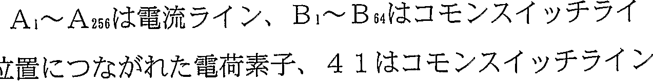
Claims
Priority Applications (2)
| Application Number | Priority Date | Filing Date | Title |
|---|---|---|---|
| EP03730504.2A EP1507251B1 (en) | 2002-05-17 | 2003-05-16 | Charge/discharge control circuit for passive matrix device |
| KR1020047018490A KR100674789B1 (ko) | 2002-05-17 | 2003-05-16 | 충방전제어회로, 발광장치 및 그 구동방법 |
Applications Claiming Priority (4)
| Application Number | Priority Date | Filing Date | Title |
|---|---|---|---|
| JP2002142432 | 2002-05-17 | ||
| JP2002-142432 | 2002-05-17 | ||
| JP2003107044A JP3498745B1 (ja) | 2002-05-17 | 2003-04-10 | 発光装置及びその駆動方法 |
| JP2003-107044 | 2003-04-10 |
Publications (1)
| Publication Number | Publication Date |
|---|---|
| WO2003098587A1 true WO2003098587A1 (en) | 2003-11-27 |
Family
ID=29552296
Family Applications (1)
| Application Number | Title | Priority Date | Filing Date |
|---|---|---|---|
| PCT/JP2003/006169 Ceased WO2003098587A1 (en) | 2002-05-17 | 2003-05-16 | Charge/discharge control circuit, light emitting device, and drive method thereof |
Country Status (7)
| Country | Link |
|---|---|
| US (1) | US6847193B2 (ja) |
| EP (1) | EP1507251B1 (ja) |
| JP (1) | JP3498745B1 (ja) |
| KR (1) | KR100674789B1 (ja) |
| CN (1) | CN100399398C (ja) |
| TW (1) | TWI253606B (ja) |
| WO (1) | WO2003098587A1 (ja) |
Families Citing this family (36)
| Publication number | Priority date | Publication date | Assignee | Title |
|---|---|---|---|---|
| JP3737889B2 (ja) * | 1998-08-21 | 2006-01-25 | パイオニア株式会社 | 発光ディスプレイ装置および駆動方法 |
| JP5191075B2 (ja) * | 2001-08-30 | 2013-04-24 | ラピスセミコンダクタ株式会社 | 表示装置、表示装置の駆動方法、及び表示装置の駆動回路 |
| TWI349903B (en) * | 2002-11-06 | 2011-10-01 | Chimei Innolux Corp | Sensing of emissive elements in an active matrix display device |
| JP4566528B2 (ja) * | 2002-12-05 | 2010-10-20 | シャープ株式会社 | 表示装置 |
| JP4734891B2 (ja) * | 2004-10-29 | 2011-07-27 | 株式会社竹屋 | 遊技機 |
| KR100736574B1 (ko) * | 2006-04-28 | 2007-07-06 | 엘지전자 주식회사 | 발광 소자 및 이를 구동하는 방법 |
| KR100818125B1 (ko) * | 2006-09-26 | 2008-03-31 | (주) 에이프로 | 액정 표시장치의 백라이트 구동회로용 방전회로 |
| KR101374507B1 (ko) * | 2006-10-31 | 2014-03-26 | 엘지디스플레이 주식회사 | 유기발광다이오드 표시장치와 그 구동방법 |
| TWI382785B (zh) * | 2007-01-09 | 2013-01-11 | Spi Electronic Co Ltd | The control circuit of the light emitting unit |
| JP4993634B2 (ja) * | 2007-03-14 | 2012-08-08 | パイオニア株式会社 | 表示装置およびその駆動方法 |
| KR100913523B1 (ko) * | 2007-12-13 | 2009-08-21 | 주식회사엘디티 | Led 표시 패널의 잔상 현상을 제거하는 led 구동장치 및 방법 |
| US7804270B2 (en) * | 2008-03-13 | 2010-09-28 | International Controls And Measurements Corp. | Motor start circuit with capacitive discharge protection |
| WO2010034509A2 (de) * | 2008-09-25 | 2010-04-01 | Tridonicatco Gmbh & Co. Kg | Verfahren zum betrieb von leuchtmitteln |
| JP5793923B2 (ja) * | 2011-04-06 | 2015-10-14 | 日亜化学工業株式会社 | 発光装置、発光装置用駆動回路及び発光装置の駆動方法 |
| TWI459351B (zh) * | 2012-05-23 | 2014-11-01 | Macroblock Inc | 點矩陣發光二極體顯示裝置之驅動系統與驅動方法 |
| JP6361096B2 (ja) * | 2013-07-31 | 2018-07-25 | 日亜化学工業株式会社 | 表示装置 |
| EP2929756B1 (de) * | 2012-12-06 | 2021-02-03 | Tridonic GmbH & Co. KG | Betriebsgerät für leuchtmittel und zugehöriges verfahren |
| DE102012023934B4 (de) | 2012-12-06 | 2022-12-01 | Tridonic Gmbh & Co Kg | Betriebsgerät und Verfahren zum Unterdrücken von Glimmen eines Leuchtmittels |
| US9343007B2 (en) * | 2013-05-21 | 2016-05-17 | My-Semi Inc. | Switch structure and method of charging and discharing scan lines of an LED display |
| JP6167794B2 (ja) * | 2013-09-20 | 2017-07-26 | 日亜化学工業株式会社 | 表示装置 |
| KR101688897B1 (ko) * | 2014-11-14 | 2016-12-22 | (주)테크레인 | 키 스캔 기능을 갖는 엘이디 구동 장치 |
| TWM512525U (zh) * | 2015-06-08 | 2015-11-21 | Hualin Prec Technology Co Ltd | 具有警示用led面板之汽車急救電源 |
| US11657774B2 (en) | 2015-09-16 | 2023-05-23 | E Ink Corporation | Apparatus and methods for driving displays |
| US10803813B2 (en) | 2015-09-16 | 2020-10-13 | E Ink Corporation | Apparatus and methods for driving displays |
| CN113241041B (zh) * | 2015-09-16 | 2024-01-05 | 伊英克公司 | 用于驱动显示器的装置和方法 |
| CN105118460B (zh) * | 2015-09-17 | 2017-10-31 | 广东欧珀移动通信有限公司 | 一种液晶显示屏的电荷释放方法及装置 |
| CN105654899B (zh) * | 2016-03-17 | 2019-05-17 | 利亚德光电股份有限公司 | 显示电路及其控制方法 |
| CN106652903B (zh) * | 2017-03-03 | 2018-10-23 | 京东方科技集团股份有限公司 | 一种oled像素电路及其驱动方法、显示装置 |
| CN107633832A (zh) * | 2017-10-25 | 2018-01-26 | 南京中电熊猫平板显示科技有限公司 | 液晶显示装置及其驱动方法 |
| US11170698B2 (en) * | 2017-11-29 | 2021-11-09 | Planar Systems, Inc. | Active discharge circuitry for display matrix |
| US10935843B2 (en) | 2019-02-08 | 2021-03-02 | Sharp Kabushiki Kaisha | Backlight and display device provided with same |
| KR102634887B1 (ko) * | 2019-04-09 | 2024-02-08 | 옵시스 테크 엘티디 | 레이저 제어를 갖는 솔리드-스테이트 lidar 송신기 |
| TWI701648B (zh) * | 2019-08-06 | 2020-08-11 | 大陸商北京集創北方科技股份有限公司 | Led顯示驅動電路、led驅動電流調製方法、及led顯示器 |
| CN110930937B (zh) * | 2019-12-19 | 2022-05-13 | 业成科技(成都)有限公司 | 显示面板及驱动方法 |
| JP7510257B2 (ja) * | 2020-02-05 | 2024-07-03 | 株式会社Kelk | 残留電荷除去装置 |
| JP2023177039A (ja) | 2022-06-01 | 2023-12-13 | シャープディスプレイテクノロジー株式会社 | 発光装置、表示装置、およびled表示装置 |
Citations (7)
| Publication number | Priority date | Publication date | Assignee | Title |
|---|---|---|---|---|
| US5838289A (en) * | 1994-10-04 | 1998-11-17 | Nippondenso Co., Ltd. | EL display driver and system using floating charge transfers to reduce power consumption |
| JPH11161219A (ja) | 1997-09-10 | 1999-06-18 | Toray Ind Inc | 発光装置駆動回路 |
| WO2000060567A1 (en) * | 1999-04-02 | 2000-10-12 | Sun Microsystems, Inc. | Method and apparatus for selective enabling of display elements, specially for arrangements with image signal propagation along a display conductor with tap points |
| EP1067505A2 (en) * | 1999-07-08 | 2001-01-10 | Nichia Corporation | Image display apparatus with light emitting elements |
| EP1091340A2 (en) * | 1999-10-05 | 2001-04-11 | Nec Corporation | Driving device and driving method of organic thin film EL display |
| US6229267B1 (en) * | 1998-09-29 | 2001-05-08 | Pioneer Corporation | Display apparatus with capacitive light-emitting devices and method of driving the same |
| US6369515B1 (en) * | 1998-09-24 | 2002-04-09 | Pioneer Corporation | Display apparatus with capacitive light-emitting devices and method of driving the same |
Family Cites Families (7)
| Publication number | Priority date | Publication date | Assignee | Title |
|---|---|---|---|---|
| US4707692A (en) * | 1984-11-30 | 1987-11-17 | Hewlett-Packard Company | Electroluminescent display drive system |
| JP3507239B2 (ja) * | 1996-02-26 | 2004-03-15 | パイオニア株式会社 | 発光素子の駆動方法及び装置 |
| JP3568097B2 (ja) * | 1998-04-22 | 2004-09-22 | パイオニア株式会社 | 発光ディスプレイ及びその駆動方法 |
| JP4576647B2 (ja) | 1999-10-12 | 2010-11-10 | 日本テキサス・インスツルメンツ株式会社 | ドットマトリクス表示装置 |
| JP3915400B2 (ja) * | 2000-11-28 | 2007-05-16 | 株式会社日立製作所 | 画像表示装置及び画像表示装置の駆動方法 |
| JP4194451B2 (ja) * | 2002-09-02 | 2008-12-10 | キヤノン株式会社 | 駆動回路及び表示装置及び情報表示装置 |
| JP2004272213A (ja) * | 2003-02-17 | 2004-09-30 | Hitachi Ltd | 画像表示装置 |
-
2003
- 2003-04-10 JP JP2003107044A patent/JP3498745B1/ja not_active Expired - Lifetime
- 2003-05-14 US US10/437,449 patent/US6847193B2/en not_active Expired - Lifetime
- 2003-05-15 TW TW092113239A patent/TWI253606B/zh not_active IP Right Cessation
- 2003-05-16 KR KR1020047018490A patent/KR100674789B1/ko not_active Expired - Fee Related
- 2003-05-16 EP EP03730504.2A patent/EP1507251B1/en not_active Expired - Lifetime
- 2003-05-16 WO PCT/JP2003/006169 patent/WO2003098587A1/ja not_active Ceased
- 2003-05-16 CN CNB038112140A patent/CN100399398C/zh not_active Expired - Fee Related
Patent Citations (7)
| Publication number | Priority date | Publication date | Assignee | Title |
|---|---|---|---|---|
| US5838289A (en) * | 1994-10-04 | 1998-11-17 | Nippondenso Co., Ltd. | EL display driver and system using floating charge transfers to reduce power consumption |
| JPH11161219A (ja) | 1997-09-10 | 1999-06-18 | Toray Ind Inc | 発光装置駆動回路 |
| US6369515B1 (en) * | 1998-09-24 | 2002-04-09 | Pioneer Corporation | Display apparatus with capacitive light-emitting devices and method of driving the same |
| US6229267B1 (en) * | 1998-09-29 | 2001-05-08 | Pioneer Corporation | Display apparatus with capacitive light-emitting devices and method of driving the same |
| WO2000060567A1 (en) * | 1999-04-02 | 2000-10-12 | Sun Microsystems, Inc. | Method and apparatus for selective enabling of display elements, specially for arrangements with image signal propagation along a display conductor with tap points |
| EP1067505A2 (en) * | 1999-07-08 | 2001-01-10 | Nichia Corporation | Image display apparatus with light emitting elements |
| EP1091340A2 (en) * | 1999-10-05 | 2001-04-11 | Nec Corporation | Driving device and driving method of organic thin film EL display |
Non-Patent Citations (1)
| Title |
|---|
| See also references of EP1507251A4 |
Also Published As
| Publication number | Publication date |
|---|---|
| JP3498745B1 (ja) | 2004-02-16 |
| CN100399398C (zh) | 2008-07-02 |
| EP1507251B1 (en) | 2013-07-17 |
| EP1507251A4 (en) | 2007-07-04 |
| TW200402017A (en) | 2004-02-01 |
| EP1507251A1 (en) | 2005-02-16 |
| US6847193B2 (en) | 2005-01-25 |
| JP2004046088A (ja) | 2004-02-12 |
| KR20050010808A (ko) | 2005-01-28 |
| US20030227278A1 (en) | 2003-12-11 |
| CN1653511A (zh) | 2005-08-10 |
| KR100674789B1 (ko) | 2007-01-25 |
| TWI253606B (en) | 2006-04-21 |
Similar Documents
| Publication | Publication Date | Title |
|---|---|---|
| WO2003098587A1 (en) | Charge/discharge control circuit, light emitting device, and drive method thereof | |
| JP5236156B2 (ja) | 有機発光ダイオード表示装置 | |
| KR100993404B1 (ko) | 정전기 보호회로 및 이를 구비한 유기전계발광 표시장치 | |
| EP1978503A2 (en) | Organic light emitting display | |
| US20090225068A1 (en) | Emission driver and organic light emitting display using the same | |
| US10490131B2 (en) | Driving control circuit for driving pixel driving circuit and display apparatus thereof | |
| JP2007522492A (ja) | アクティブマトリクスによる電界発光表示装置 | |
| EP2144222A1 (en) | Light emitting diode display device | |
| CN110176214B (zh) | 像素驱动电路以及有机电致发光显示器 | |
| US7880699B2 (en) | Method for driving pixels of an organic light emitting display | |
| CN100378781C (zh) | 显示面板及其驱动方法 | |
| US12112691B2 (en) | Display module including a display panel and driving circuit | |
| KR100568592B1 (ko) | 일렉트로-루미네센스 표시장치와 그의 구동방법 | |
| JP2004126285A (ja) | 有機エレクトロルミネッセンス素子の発光駆動回路及び表示装置 | |
| KR100628277B1 (ko) | 유기전계발광표시장치 및 이의 구동방법 | |
| KR100702094B1 (ko) | 액티브 매트릭스형 표시 장치 및 그 구동 방법 | |
| US20060244388A1 (en) | Emission control driver and organic light emitting display having the same | |
| KR20100072509A (ko) | 유기발광다이오드표시장치 및 그 구동방법 | |
| CN113948032A (zh) | 像素电路及其驱动方法 | |
| CN100428312C (zh) | 电致发光显示装置及其驱动方法 | |
| US7893894B2 (en) | Organic light emitting display and driving circuit thereof | |
| CN115662350B (zh) | 电源电压控制电路、像素电路、驱动电路及显示面板 | |
| KR100793555B1 (ko) | 발광 표시장치 | |
| JP5594977B2 (ja) | 画像表示装置 | |
| US20250140204A1 (en) | Driving circuit |
Legal Events
| Date | Code | Title | Description |
|---|---|---|---|
| AK | Designated states |
Kind code of ref document: A1 Designated state(s): CN KR |
|
| AL | Designated countries for regional patents |
Kind code of ref document: A1 Designated state(s): AT BE BG CH CY CZ DE DK EE ES FI FR GB GR HU IE IT LU MC NL PT RO SE SI SK TR |
|
| 121 | Ep: the epo has been informed by wipo that ep was designated in this application | ||
| WWE | Wipo information: entry into national phase |
Ref document number: 2003730504 Country of ref document: EP Ref document number: 1020047018490 Country of ref document: KR |
|
| WWE | Wipo information: entry into national phase |
Ref document number: 20038112140 Country of ref document: CN |
|
| WWP | Wipo information: published in national office |
Ref document number: 1020047018490 Country of ref document: KR |
|
| WWP | Wipo information: published in national office |
Ref document number: 2003730504 Country of ref document: EP |