WO2003104886A1 - 波長分割多重光再生システム及び波長分割多重光再生方法 - Google Patents
波長分割多重光再生システム及び波長分割多重光再生方法 Download PDFInfo
- Publication number
- WO2003104886A1 WO2003104886A1 PCT/JP2003/007433 JP0307433W WO03104886A1 WO 2003104886 A1 WO2003104886 A1 WO 2003104886A1 JP 0307433 W JP0307433 W JP 0307433W WO 03104886 A1 WO03104886 A1 WO 03104886A1
- Authority
- WO
- WIPO (PCT)
- Prior art keywords
- optical
- pulse
- fiber
- light
- soliton
- Prior art date
- Legal status (The legal status is an assumption and is not a legal conclusion. Google has not performed a legal analysis and makes no representation as to the accuracy of the status listed.)
- Ceased
Links
Classifications
-
- H—ELECTRICITY
- H04—ELECTRIC COMMUNICATION TECHNIQUE
- H04B—TRANSMISSION
- H04B10/00—Transmission systems employing electromagnetic waves other than radio-waves, e.g. infrared, visible or ultraviolet light, or employing corpuscular radiation, e.g. quantum communication
- H04B10/29—Repeaters
- H04B10/291—Repeaters in which processing or amplification is carried out without conversion of the main signal from optical form
- H04B10/299—Signal waveform processing, e.g. reshaping or retiming
-
- H—ELECTRICITY
- H04—ELECTRIC COMMUNICATION TECHNIQUE
- H04B—TRANSMISSION
- H04B10/00—Transmission systems employing electromagnetic waves other than radio-waves, e.g. infrared, visible or ultraviolet light, or employing corpuscular radiation, e.g. quantum communication
- H04B10/25—Arrangements specific to fibre transmission
- H04B10/2507—Arrangements specific to fibre transmission for the reduction or elimination of distortion or dispersion
- H04B10/25077—Arrangements specific to fibre transmission for the reduction or elimination of distortion or dispersion using soliton propagation
-
- G—PHYSICS
- G02—OPTICS
- G02F—OPTICAL DEVICES OR ARRANGEMENTS FOR THE CONTROL OF LIGHT BY MODIFICATION OF THE OPTICAL PROPERTIES OF THE MEDIA OF THE ELEMENTS INVOLVED THEREIN; NON-LINEAR OPTICS; FREQUENCY-CHANGING OF LIGHT; OPTICAL LOGIC ELEMENTS; OPTICAL ANALOGUE/DIGITAL CONVERTERS
- G02F1/00—Devices or arrangements for the control of the intensity, colour, phase, polarisation or direction of light arriving from an independent light source, e.g. switching, gating or modulating; Non-linear optics
- G02F1/35—Non-linear optics
- G02F1/3511—Self-focusing or self-trapping of light; Light-induced birefringence; Induced optical Kerr-effect
- G02F1/3513—Soliton propagation
Definitions
- the present invention relates to a wavelength division multiplexing optical regeneration system and a wavelength division multiplexing optical regeneration method.
- the transmission capacity of communication systems is steadily increasing, and the transmission capacity is increasing remarkably by optical communication systems using optical fibers.
- communication systems are divided into point-to-point trunk systems, metro systems, and access systems.
- Optical communication systems have already become widespread in the former trunk systems, and optical communications systems have also been used in the latter.
- the transition to communication systems is underway. That is, the entire communication system is being constructed by an optical communication system.
- the amount of information that can be transmitted over a single optical fiber has increased dramatically due to wavelength division multiplexing. In this method, the low-loss band of the optical fiber is converted to the spectral conversion efficiency.
- the transmission capacity that can be transmitted with one optical fiber is about 3.2 Tbit / s.
- this transmission capacity is realized by 320 channels, assuming that the signal light transmission speed of each channel (wavelength) is 10 Gbit / s currently used.
- This optical signal reproduction system includes, for example, a receiving device that receives deteriorated signal light and converts it into an electric signal, and a desired reproduction such as amplification, noise removal, waveform reproduction, and clock reproduction for the electric signal.
- 3200 corresponds to the number of channels.
- One optical receiving device, a reproducing device, and a transmitting device are incorporated.
- Such an optical signal reproduction system including a large number of devices has problems that it is difficult to reduce the size and that the power consumption is large.
- the reproducing apparatus used in the above-mentioned optical signal reproducing system is an electric device for processing an electric signal, and has a physical upper limit of response speed.
- the transmission speed limit of signals that can be processed by electrical devices is currently 40 Gbit / s, and this transmission speed still requires about 80 channels. Furthermore, high power is required to drive electrical devices at such high speeds. Therefore, in an optical signal regeneration system using an electric device, the transmission speed of each channel has an upper limit, and in reality, it is difficult to reduce the size and power consumption of the channel.
- One of the methods to solve the problems in the optical signal regeneration system using such an electric device is to convert the signal light into an electric signal without converting the signal light into an electric signal.
- a device using the all-optical signal reproducing method generally includes a high-speed electric modulator and a reproducing device utilizing a nonlinear optical effect of a substance.
- this all-optical signal reproducing apparatus uses an electric modulator, there is an upper limit to the processing speed as in the optical signal reproducing system that performs photoelectric conversion.
- the all-optical signal reproducing apparatus described above uses a nonlinear optical response (nonlinear optical effect) for reproducing an optical signal. In that case, the following problem also occurs.
- the polarization state of each signal light included in the propagated wavelength division multiplexed light is Slightly different for each wavelength.
- the nonlinear optical effect is determined according to the polarization state of the incident light. Since the magnitude greatly changes, the reproduced wavelength division multiplexed light includes a signal light that is not reproduced well or that is not reproduced at all.
- Light generation refers to the function of re-amplifying, re-shaping and re-timing (hereinafter abbreviated as 03R) the intensity, waveform shaping, and timing reproduction of an optical signal degraded by transmission.
- 03R re-amplifying, re-shaping and re-timing
- An optical regeneration system with this function can enable infinite (long-distance) optical fiber transmission.
- the infinite (long-distance) transmission described above is reported by Leuthold et al. (Le PC leakage 33 uthold et al., Electron. Lett., 38, p. 890, 2002). This report describes 40 Gb / s 1,000,000 km transmission using the 03R regenerator.
- Leuthold et al Used electronic circuit technology for extracting the optical clock required for time recovery (technology for generating a clock pulse train synchronized with the transmitted signal light) and for switching. For this reason, this device cannot handle transmission speeds that cannot be handled by electronic circuit technology. It cannot be applied to systems with transmission speeds exceeding the electronic circuit limit, such as 160 Gb / s systems. As for the 160 Gb / s system, an optical regeneration system using an optical switch has been reported (Schubert et al., Electron. Lett., 38, p. 903, 2002). However, this system cannot function as a 03R device because it does not have a clock extraction device. To summarize the above, the 03R based on effective all-optical technology has not yet been realized.
- the other is a method based on the self-phase modulation effect of optical pulses through an optical fiber nonlinear element (Mamyshev, EC0C, 98, p. 475, 1998).
- This is called the Mamyshev filter because of the proposer's name.
- the method of utilizing the supercontinuum light is positioned as a pursuit type of this.
- the latter (Mamyshev filter) is used in the 1,000,000 km transmission line of Leuthold et al.
- the mainstream of this technology is a combined method of optical clock extraction and optical switch technology.
- This configuration is shown in Figure 38. It consists of an optical clock extractor and an optical switch.
- the former optical clock extraction unit determines the phase of the input signal (optical signal or electric signal corresponding to the transmission signal) and the phase of local light (optical pulse train that can be a clock reference, also called optical local oscillator (optical L0)). It is to match.
- optical clock extraction is achieved by synchronizing the input light and the local light. Therefore, the light L0 needs to have repetitive frequency variability.
- optical switch section is an optical device that utilizes nonlinear effects in an optical fiber to realize a multiplication function in the optical domain, such as a four-wave mixing (FWM) device or a nonlinear optical loop mirror (.
- FWM four-wave mixing
- N0LM nonlinear optical loop mirror
- FIG. 38 a portion surrounded by a broken line is an optical extractor, which includes an optical phase comparator, an optical L0 generator, and a controller circuit.
- the optical phase comparator detects the phase difference between the external signal light and light L0, and reduces the oscillation frequency of light L0 so that the error is reduced. (Corresponding to the pulse train repetition frequency).
- a pulse train (hereinafter referred to as a clock pulse train) whose time position synchronized with the external signal is accurate can be obtained as an output.
- a phase comparator that can operate at high speeds exceeding 160 GHz is realized.
- Such a synchronization method using a phase comparator in the optical domain is called an optical phase locked loop (OPLL).
- OPLL optical phase locked loop
- Timing jitter means the amount of shift in the time position of a clock pulse. This suppression is important because this jitter can cause deterioration of the transmission system's “I” performance.
- the timing jitter of the clock pulse train is correlated with the 0PLL operation speed. Jitter is reduced, ie, 0PLL speed-up is effective for jitter reduction
- NOLM is used as in the above technology (Bigo et al, US6, 239, 893 Bl)
- the OPLL loop becomes long. In order to solve this, it is important to shorten the fiber length of the optical nonlinear device used in the phase comparator.
- the 0PLL operation band is not limited, in other words, the high-speed operation of the 0PLL is realized, and a high-quality quick pulse train with low jitter can be generated.
- an optical switch technology which describes a method of utilizing FWM, which is a typical example of an optical switch that utilizes the nonlinear effect of an optical fiber. You Then, if any of the input light has sufficient optical power for the nonlinear effect, a new light wave different in color from them will be generated. This is the FWM phenomenon.
- a clock pulse train and signal light are input to an optical fiber, not only the information of the input signal light is superimposed on the FWM generated light, but also the pulse timing is determined by the click pulse train.
- the pulse-rectification technology that is effective for suppressing the increase in intensity noise in the optical switch, which is related to (1) the device that converts the optical pulse waveform into a waveform suitable for the optical switch.
- the time fluctuation (phase fluctuation) of an input transmission signal pulse is converted into the time fluctuation-reproduced output signal light intensity fluctuation.
- Figure 39A an optical switch of a pulse train having a jitter and a clock pulse train is considered.
- Optical switch output pulse power correlates with time overlap of transmitted pulse and clock pulse There is.
- the change in pulse overlap due to jitter is converted to optical switch output pulse power fluctuation.
- the rectangular conversion of the transmission signal light pulse or the extracted clock pulse is effective (Fig. 39B).
- the methods for making this rectangle can be broadly classified into a method that utilizes chromatic dispersion and polarization dispersion, and a method that utilizes the combined effect of nonlinear and normal dispersion.
- the former example is a method using a fiber Bragg grating or polarization maintaining fiber (Lee et al., 0FC2001, PD30-1, 2001 and Schubert et al., Electron. Lett., 38, p. 903, 2002).
- the latter example uses a normal dispersion fiber (Nakatsuka et al., Phys. Rev. Lett., 47, p. 910, 1981).
- the sharpness of the falling and rising edges of the rectangle to be converted is determined by the input pulse width. That is, in order to obtain a steep rectangular pulse, it is necessary to input a corresponding ultrashort light pulse.
- the latter has the advantage that the waveform can be converted into a sharp rectangular wave, but in order to obtain the nonlinear effect and dispersion effect required for the rectangularization, a high power of the input light is required. It is necessary to increase the length of the fiber.
- ASE spontaneous emission light
- noise has an optical spectrum wider than the signal light, so that noise components outside the signal light band can be removed to some extent by the optical filter. However, noise components in the signal light band remain.
- SRS stimulated Raman scattering
- Fig. 4 OA shows the configuration of the noise elimination device. It consists of an anomalous-dispersion fiber (ADF) and an optical filter. An optical soliton having a noise component as shown in the upper part of Fig. 40B is input to the ADF. In the propagation there, the optical soliton component is SSFS by SRS. It should be noted here that the SRS shifts the soliton component to the longer wavelength side, but does not shift the noise component to the longer wavelength side.
- ADF anomalous-dispersion fiber
- SRS shifts the soliton component to the longer wavelength side, but does not shift the noise component to the longer wavelength side.
- an object of the present invention is to solve these problems and provide a simple 03R system.
- the present invention solves the above-mentioned problems, and achieves a large transmission capacity, miniaturization, and power saving. It is an object of the present invention to provide a wavelength division multiplexing optical regenerating system and a wavelength division multiplexing optical regenerating method which can be realized and can reproduce all the signal light in the wavelength division multiplexing light. Disclosure of the invention
- Seo Li Tong 3 N'nota (Soliton Converter), Nono 0 Noresurora (Pulse Roller), Khasi Yatta (Kerr- shutter), or
- This is an optical regeneration system that is equipped with a regeneration device that has at least one device among the soliton purifiers and that reproduces degraded signal light.
- optical regenerating system of the present invention is an optical regenerating system in which a polarization converter is provided before the reproducing apparatus or inside the reproducing apparatus.
- a demultiplexer is provided in a stage preceding the reproducing device, or in a case where the polarization converter is provided in a stage preceding the reproducing device, in a stage preceding the polarization converter. It is an optical reproduction system provided.
- optical regenerating system of the present invention is an optical regenerating system provided with a multiplexing device after the reproducing device.
- optical regeneration system of the present invention includes: a stage preceding the reproducing device; a stage preceding the polarization converter when the polarization converter is provided in a stage preceding the reproducing device; or
- the optical regenerating system includes a dispersion compensator in the preceding stage of the demultiplexing device.
- optical regeneration system including, on an emission side of the reproduction device, a multiplexing device that multiplexes the signal light reproduced by the reproduction device and another signal light.
- Another aspect of the optical reproduction system of the present invention is an optical reproduction system in which the reproduction devices are connected in multiple stages.
- optical reproduction system of the present invention is an optical reproduction system in which an optical switch is provided between the reproduction apparatuses connected in multiple stages.
- optical reproducing system of the present invention is an optical reproducing system for adjusting input power at a stage prior to the reproducing apparatus.
- a first aspect of the waveform shaper of the present invention is a waveform shaper provided with a soliton converter having an anomalous-dispersion fiber (ADF) whose fiber length is equal to or less than twice the soliton period. .
- ADF anomalous-dispersion fiber
- waveform shaper of the present invention is a waveform shaper provided with an optical filter at a stage subsequent to the anomalous dispersion fiber.
- waveform shaper of the present invention is a waveform shaper provided with an optical amplifier at a stage preceding the anomalous dispersion fiber.
- waveform shaper of the present invention is a waveform shaper provided with a Mamyshev filter or N0LM instead of the soliton converter.
- Another embodiment of the waveform shaper of the present invention is a waveform shaper provided with a pulse compressor on the incident side.
- the pulse compressor is a waveform shaper using an adiabatic compression method.
- Another aspect of the waveform shaper of the present invention is a waveform shaper using a dispersion reducing fiber whose dispersion characteristic decreases in a longitudinal direction of an optical fiber as the pulse compressor.
- waveform shaper of the present invention is a waveform shaper in which the pulse compressor has a profile having a step-like dispersion characteristic in the longitudinal direction of the optical fiber.
- waveform shaper of the present invention is a waveform shaper in which a CDPF having a profile having a comb-like dispersion characteristic in the longitudinal direction of the optical fiber is used as the pulse compressor.
- a waveform shaper using an optical fiber having a non-linear characteristic increasing in a longitudinal direction, as the pulse compressor is also included in the waveform shaper.
- Another aspect of the waveform shaper of the present invention is a waveform shaper using an optical fiber having a stepwise profile having a non-linear characteristic in a longitudinal direction as the pulse compressor.
- the aspect of the invention is that the pulse compressor has a nonlinear characteristic in the longitudinal direction.
- This is a waveform shaper using an optical fiber having a comb-like profile.
- waveform shaper of the present invention is a waveform shaper provided with a Raman amplifier in the pulse compressor.
- Another embodiment of the waveform shaper of the present invention is a waveform shaper using a saturable absorber having a saturable absorption characteristic instead of the soliton converter.
- waveform shaper of the present invention is a waveform shaper provided with a position adjustment mechanism that adjusts a position of the saturable absorber to vary a saturable absorption characteristic.
- Another embodiment of the waveform shaper of the present invention is a waveform shaper in which the saturable absorption characteristic has an in-plane distribution.
- a first embodiment of the car shirt according to the present invention is a car shirt equipped with a duplexer, an optical phase-locked loop (OPLL), and an optical switch unit.
- OPLL optical phase-locked loop
- the bit rate difference in the 0 PLL is ⁇ , and the loop length is! ⁇ . .
- ⁇ be the velocity of light in the optical fiber, and the length of the fiber connecting the demultiplexer and the optical switch! ⁇ ⁇
- ⁇ is the refractive index of the optical fiber
- X is an arbitrary number
- L L. . P is, ⁇ ⁇ (L L oop) Ku v 'X / n' L A - a car shutter, wherein a relationship of B is determined to stand become.
- Another aspect of the car shirt according to the present invention includes: an optical L0 generator that generates an optical L0 signal in the 0 PLL; a phase comparator that detects a phase difference between an externally input signal light and the optical L0 signal; And a control unit for adjusting the frequency of the light L0 signal based on the phase difference.
- Another embodiment of the car shirt according to the present invention is a car shirt provided with an FWM unit for generating FWM light, an optical filter, and a light receiving unit in the optical phase comparator.
- Another embodiment of the car shirt according to the present invention is a car shirt in which any one of a highly non-linear optical fiber, PPLN (Periodically-poled LiN03) or SOA (Semi-conductive Optical Amplifier) is used in the FWM part.
- PPLN Periodically-poled LiN03
- SOA Silicon-conductive Optical Amplifier
- Another aspect of the car shirt according to the present invention is the car shirt described in that the light receiving unit is provided with a pulse roller in a preceding stage, and monitors a frequency characteristic of a pulse incident on the light receiving unit.
- Another embodiment of the car shutter according to the present invention is a car shutter in which the LO generator is provided with a beat light generator.
- the beat light generator comprises: one or more semiconductor lasers having two or more frequency components for generating CW light; and an optical coupler for multiplexing the CW light.
- a car shutter provided with:
- Another embodiment of the car shutter of the present invention is a car shutter in which the semiconductor laser is driven in series.
- Another embodiment of the car shutter of the present invention is a car shutter provided with an optical fiber compressor between the beat light generator and the optical switch section.
- the phase comparator includes a PD (Photo Diode), a Loop Filter, and an LD control unit, and the PD generates a photocurrent by two-photon absorption. It is a car shirt.
- the PD is a car shirt using a silicon avalanche photodiode (SiAPD).
- SiAPD silicon avalanche photodiode
- Another embodiment of the car shirt according to the present invention is a car shirt provided with an optical switch section, an FWM section, an optical filter, and a phase adjusting section.
- Another aspect of the car shutter according to the present invention is a car shutter in which the phase adjustment unit is controlled so that the amount of phase adjustment does not change in response to a change in environmental temperature.
- Another embodiment of the car shutter according to the present invention is a car shutter in which the phase adjustment amount is feedback-controlled based on an output pulse.
- the frequency interval of the pump light and the signal light delta [nu (the detuning), and the spectral width delta V [rho input pump pulse, the input signal pulse scan Bae This is a car shirt having the following relationship between the vector width A v s and.
- Another embodiment of the car shutter of the present invention is a car shutter in which the length L is determined by the following equation in the FWM section.
- L NL Another embodiment of the car shutter of the present invention is a car shutter in which the length L is determined by the following equation in the FWM section.
- an FWM unit provided in the optical phase comparator and an FWM unit provided in the optical switch unit are shared, and further, an optical L0 generator and a control unit are provided.
- This is a car shirt equipped with.
- a first aspect of the pulse roller of the present invention is a pulse roller provided with a pulse roller fiber having highly nonlinear characteristics.
- Another embodiment of the pulse roller according to the present invention is a pulse roller in which the pulse roller fiber is a normal dispersion increasing fiber having a characteristic that a normal distribution value increases in a longitudinal direction.
- pulse roller fiber is an optical fiber having a characteristic that a nonlinear value decreases in a longitudinal direction.
- Another embodiment of the pulse roller of the present invention is a pulse roller comprising a dispersion management optical fiber in which two or more types of optical fibers having different normal dispersion characteristics and nonlinear characteristics in a longitudinal direction are combined.
- Another aspect of the pulse roller of the present invention is the dispersion management optical fiber, wherein the pulse roller has an optical fiber in which a dispersion effect is dominant in a longitudinal direction and an optical fiber in which a nonlinear effect is dominant in a longitudinal direction. is there.
- Another aspect of the pulse roller of the present invention is the dispersion management optical fiber, wherein the dispersion characteristic of the optical fiber in which the dispersion effect is dominant and the nonlinear characteristic of the optical fiber in which the nonlinear effect is dominant are step-shaped.
- This is a pulse roller that is arranged to be a portal file.
- Another embodiment of the pulse roller of the present invention is the dispersion management light:
- the pulse roller is arranged so that the dispersion characteristic of the optical fiber in which the dispersion effect is dominant and the nonlinear characteristic of the optical fiber in which the nonlinear effect is dominant change into a comb-shaped profile.
- a first aspect of the 0TDM signal generator of the present invention is a 0TDM signal generator provided with a pulse roller and an optical switch.
- a first embodiment of the soliton pillifier of the present invention is a soliton purifier in which a soliton fiber is arranged between two optical filters.
- Another embodiment of the soliton puurifier of the present invention is a soliton purifier that controls a slope (gain slope) of a gain due to stimulated Raman scattering in the soliton fiber and realizes a wavelength shift of the soliton. .
- the soliton fiber is a soliton fiber which is a highly nonlinear fiber.
- Another embodiment of the present invention is a soliton purifier which is provided with a pump light generator for generating external pump light and generates stimulated Raman scattering by the external pump light.
- Another embodiment of the soliton pillifier of the present invention is a soliton pillifier further provided with a pulse compressor on the incident side.
- Another embodiment of the soliton pillifier of the present invention is a soliton pillifier that generates stimulated Raman scattering while performing adiabatic compression of the soliton.
- the first aspect of the soliton noise control method according to the present invention is a method for controlling a predetermined noise amplification in an optical nonlinear signal processing using an optical soliton train, by using a duty ratio (a ratio of a pulse interval to a pulse width) and a dispersion distance.
- This is a soliton noise control method that determines the maximum propagation distance in gain.
- Another embodiment of the soliton noise control method of the present invention is a soliton noise control method using a CS-RZ pulse sequence as a modulation method.
- a first aspect of the optical transmission system of the present invention is an optical transmission system in which optical regeneration systems are connected in multiple stages in series.
- FIG. 1 is a schematic configuration diagram of a wavelength division multiplexing optical regeneration system according to a first embodiment of the present invention.
- FIG. 2 is a schematic configuration diagram of a playback device 15 included in the playback system of FIG.
- FIG. 3 is a schematic configuration diagram of the clock reproducing device 21 included in the reproducing device 15 of FIG.
- FIG. 4 is a schematic configuration diagram of another clock reproducing device 21 included in the reproducing device 15 of FIG.
- FIG. 5 is a schematic configuration diagram of a waveform reproducing device 19 included in the reproducing device 15 of FIG.
- FIG. 6 is a schematic configuration diagram of another waveform reproducing device 19 included in the reproducing device 15 of FIG.
- FIG. 7 is a schematic configuration diagram of a polarization converter 13 included in the reproduction system of FIG. 1.
- FIG. 8 is a schematic configuration diagram of another polarization converter 13 included in the reproduction system of FIG.
- FIG. 9 is a schematic configuration diagram of another polarization converter 13 included in the reproduction system of FIG.
- FIG. 10 is a schematic configuration diagram of one embodiment of the polarization converter 13 of FIG.
- FIG. 11 is a schematic configuration diagram of another embodiment of the polarization converter 13 of FIG.
- FIG. 12 is a schematic configuration diagram of still another embodiment of the polarization converter 13 of FIG.
- FIG. 13 is a schematic configuration diagram of a wavelength division multiplexing optical regeneration system according to the second embodiment of the present invention.
- FIG. 14 is a schematic configuration diagram of a wavelength division multiplexing optical regeneration system according to the third embodiment of the present invention.
- FIG. 15 is a schematic configuration diagram of a wavelength division multiplexing optical regeneration system according to the fourth embodiment of the present invention.
- FIG. 16 is a schematic configuration diagram of a wavelength division multiplexing optical regeneration system according to the fifth embodiment of the present invention.
- FIG. 17 is a configuration diagram of a playback device according to the present invention.
- Fig. 18 is a block diagram of the soliton converter in Fig. 17
- FIG. 19 is a schematic configuration diagram showing another form of the soliton converter of FIG. 17.
- FIG. 2OA is a graph showing an optical signal-to-noise ratio 0SNR of an output pulse from the soliton converter.
- Figure 2 0 B is a graph showing a soliton order ⁇ dependence of spectral line broadening factor ⁇ w / ⁇ ⁇ i ⁇ .
- Figure 2 1 shows the input power P i n depends ⁇ raw output pulse autocorrelation wave ⁇ delta t A c from soliton converter.
- the left graph portion before the input of the output optical filter, Dara off the right part is the output pulse autocorrelation trace width delta t A c after the output of the output optical filter.
- 2 2 left graph, 0, 2 0, 4 0 and 8 0 m long pulse after SMF propagation, central graph ⁇ Pi right graph when the adjustments of the P i n 7 is an autocorrelation waveform of an output pulse from the soliton converter of FIG.
- the middle graph is before input of the output optical filter, and the right graph is after output of the output optical filter.
- 6 is a graph showing the dependence of OSNR on n .
- FIG. 24 is a configuration diagram of a Kerr-shutter.
- FIG. 25A is a graph showing the timing jitter characteristic I 1 when the LD pair is driven independently.
- Fig. 25B is a graph showing the timing jitter characteristics during serial driving.
- FIG. 26A is a configuration diagram of the light receiving unit.
- FIG. 26B is a modification of FIG. 25A.
- FIG. 26C is a further modification of FIG. 26A.
- Fig. 27 is another configuration diagram of the Kerr-shutter, which shows the FW of the phase comparator and the optical switch.
- FIG. 28 is a configuration diagram of a pulse roller.
- Figure 29A shows the dispersion profile of a normal dispersion-enhanced fiber.
- Figure 29B shows the dispersion profile of the step-shaped dispersion profile fiber.
- Figure 29C shows the dispersion profile of the comb-shaped dispersion profile fiber.
- FIG. 3OA is a block diagram of a pulse roller, and shows a pulse rectangularization transmission line.
- FIG. 30B shows a dispersion profile of the pulse roller fiber of FIG. 3OA.
- FIG. 31 is a graph showing the results of the pulse propagation simulation in FIGS. 3OA and 3OA.
- FIG. 32 is a configuration diagram of a time reproducing apparatus or a time dividing apparatus including a pulse roller and an optical switch unit.
- FIG. 33 is a block diagram of a clock extractor in which a pulse roller and an OPL L are combined.
- FIGS. 34A and B show the time waveform and output characteristics of the pulse output from the pulse roller.
- FIGS. 35A and B show a light receiving unit for recognizing a phase difference.
- FIG. 36A is a configuration diagram of a soliton purifier.
- FIG. 36B shows an example using HNLF for soliton purifier.
- FIG. 36C shows an example in which Raman amplification is used for the soliton purifier.
- Figure 37 is a graph illustrating the gain slope in the soliton band.
- FIG. 38 is an explanatory diagram relating to a conventional time reproduction technique.
- FIGS. 39A and 39B are explanatory diagrams of a conventional pulse rectangularization technique.
- FIG. 4OA is a configuration diagram of a conventional noise elimination device.
- FIG. 40B is a graph showing a noise removal mechanism.
- FIG. 41A is a waveform diagram showing an input pulse.
- FIGS. 41B to 41D are waveform diagrams in which FIG. 41A is converted into a rectangular pulse.
- FIG. 42 is a waveform chart showing the relationship between pulse intensity and instantaneous frequency.
- FIG. 43 is a configuration diagram of a reproduction system according to the present invention.
- FIG. 44 is a configuration diagram of a reproduction system according to the present invention.
- FIG. 45 is a configuration diagram of a playback device according to the present invention.
- FIG. 46 is a block diagram showing a reproducing system using the reproducing apparatus according to the present invention.
- FIG. 47 is a graph showing the relationship between the input light intensity and the output light intensity of the saturable absorber.
- FIG. 48 is a configuration diagram of a device using a saturable absorber.
- FIG. 49 is a block diagram showing a modification of the device of FIG.
- FIG. 50 is a block diagram showing a further modification of the device of FIG.
- FIG. 51A is a diagram showing an input pulse and an output pulse in the FWM when the horizontal axis represents time.
- FIG. 51B is a diagram illustrating an input pulse and an output pulse in the FWM when the horizontal axis indicates frequency.
- Fig. 52 is a graph showing the relationship between the bandwidth required for FWM and the fiber length.
- Fig. 53 is a flow chart illustrating one design method for determining the optimal fiber length in FWM. .
- FIG. 54 is an experimental configuration diagram in which the fiber length is optimized according to the flowchart of FIG. 53 and wavelength conversion is performed by FWM.
- FIG. 55 is a graph showing input / output pulse waveforms obtained in the experiment of FIG.
- FIG. 56 is a graph showing the autocorrelation waveform at the time of input / output according to the experiment of FIG.
- FIG. 57 is a configuration diagram of a waveform shaper using FWM and SPM.
- FIG. 58 is a graph showing a pulse waveform in the waveform shaper.
- FIG. 59 is a graph showing the relationship between the input pump power and the output FWM power in the waveform shaper of FIG.
- FIG. 6OA is an example of a configuration for detecting a phase difference without using an optical fiber in the FWM unit.
- FIG. 60B shows a modification of the FWM unit.
- FIG. 61 is a graph illustrating a method of temporally changing the amplitude of a rectangular pulse in the OPLL operation.
- FIG. 62 is a configuration diagram of the OTDM signal generator according to the present invention.
- FIG. 63 is an explanatory diagram showing the relationship between the amplification gain of the Raman amplifier and the spectrum of the soliton.
- Fig. 64 is a graph showing the peak gain of noise amplification obtained by numerical calculation for the bit rate and the propagation distance.
- FIG. 65 is a graph showing the spectrum of the output pulse train when the repetition frequency is 32 O GHz and the propagation distance is l km in FIG.
- FIG. 66 is a configuration diagram showing the polarization maintenance of a device using the nonlinear effect.
- Fig. 67 shows the input and output when an optical soliton train with a repetition frequency of 160 GHz and a half width at lps is propagated to a 2 km HLF. It is a graph showing a vector.
- Fig. 68 is a modification of the Kerr-shutter shown in Fig. 24.
- the fiber length from the first demultiplexer to the optical switch is almost the same between the case where the fiber is passed through the OPLL and the case where it is directly.
- FIG. 3 is a schematic configuration diagram showing that the lengths are the same.
- Figure 69 is a graph showing the relationship between the length (distance) of the HNLF used in Figure 67 and the variance.
- FIG. 70 is a schematic configuration diagram showing an optical transmission system in which the reproduction systems shown in FIG. 1 are connected in multiple stages in series.
- the wavelength division multiplexed light including the degraded signal light is reproduced using the nonlinear optical effect as described later. Therefore, the nonlinear optical effect will be described first.
- the nonlinear optical effect occurs remarkably when light with high intensity enters a medium having a large nonlinear optical constant (hereinafter also referred to as a nonlinear optical medium).
- examples of the medium having a large nonlinear optical constant include an optical fiber (hereinafter, also referred to as a highly nonlinear fiber) doped with germanium, fluorine, a rare earth element, and the like, a ferroelectric material such as LiNb03, a semiconductor, and the like. .
- the signal light itself, or Examples of the control light include one or more control lights or pump lights prepared to generate this effect separately from the signal light.
- the nonlinear optical effect occurs, for example, a change in the waveform of the signal light incident on the medium or a modulation of the phase thereof occurs.
- a harmonic, a difference frequency, or a sum frequency having a different frequency from the control light or the excitation light is generated.
- nonlinear optical effects include self-phase modulation (hereinafter referred to as SPM), cross-phase modulation (hereinafter referred to as XPM) or four-wave mixing (hereinafter referred to as FWM), Raman amplification, parametric amplification, soliton Effects and the supercontinuum effect (hereinafter referred to as SC).
- SPM self-phase modulation
- XPM cross-phase modulation
- FWM four-wave mixing
- Raman amplification Raman amplification
- parametric amplification soliton Effects
- soliton Effects soliton Effects
- SC supercontinuum effect
- the magnitude of the nonlinear optical effect for example, the degree of frequency modulation and the intensity of generated harmonics are nonlinear with respect to the intensity of incident light.
- the magnitude of the nonlinear optical effect has polarization dependence. For example, consider a case in which high intensity light is not unpolarized light but has a certain polarization state, and the nonlinear optical medium has anisotropy in a plane orthogonal to the incident direction of the high intensity light. . In this case, the magnitude of the non-linear optical effect has polarization dependency that it depends on the polarization state of the light and the relative orientation of the medium. Even when the medium does not have such anisotropy, the magnitude of the nonlinear optical effect is such that when the light with high intensity is the control light or the excitation light, the polarization state of the signal light and the control light or the control light It strongly depends on the relative relationship between the excitation light and the polarization state.
- embodiments of the present invention will be described with reference to the drawings.
- FIG. 1 shows a wavelength division multiplexing optical reproduction system 1 (hereinafter, referred to as a reproduction system 1) according to a first embodiment of the present invention.
- the regenerating system 1 is installed in a wavelength division multiplexing communication system, for example, an optical fiber 4 and an optical fiber 6 which constitute a part of the optical transmission system. Used in a closed state.
- the reproduction system 1 transmits the signal light included in the wavelength division multiplexed light, which has been deteriorated by the propagation of the wavelength division multiplexed light through the transmission path of the wavelength division multiplexing communication system, before the propagation.
- the state is restored or reproduced, for example, the state immediately after emission from the transmitter.
- the deterioration of the signal light means that, for example, the intensity, phase, frequency, polarization state, or a plurality of these change over a predetermined allowable range.
- the reproduction system 1 includes a demultiplexer 8 and a multiplexer 10.
- the demultiplexer 8 has one input port 8a and a plurality of output ports, and the optical fiber 4 is connected to the input port 8a.
- the wavelength division multiplexed light that has entered the demultiplexer 8 from the optical fiber 4 via the input port 8a is demultiplexed into a plurality of signal lights ⁇ 2 , ⁇ 3 ,..., L n .
- Each of the signal lights # 2 , # 2 , # 3 , ... is output from the output port of the demultiplexer 8 which differs for each wavelength.
- a dispersion compensator 300 for compensating for the added added by the dispersion of the transmission line before the demultiplexing. This form is shown in FIG.
- dispersion compensators are commonly used modules such as modules using fiber Bragg gratings, modules using ET ports, DCF (Dispersion shifted fiber) modules, modules using prism pairs and gratings, etc. What has been applied is applicable. Note that the dispersion compensator 300 described above may be either a fixed type or a variable type, but the variable type is advantageous because the range of chirp compensation is expanded.
- the multiplexer 10 has a plurality of input ports and one output port 10a, and an optical fiber 6 is connected to the output port 10a.
- the signal light is incident on the multiplexing device 1 0 and via the input port; L have tut 2, ⁇ 3, ' ⁇ ⁇ ⁇ , are multiplexed becomes wavelength divider multiplexed light, the output port 1 0 a Through the optical fiber 6.
- Each of the demultiplexing device 8 and the multiplexing device 10 can be constituted by, for example, an arrayed waveguide diffraction grating, a filter type multiplexing / demultiplexing device, or an FBG (Fiber Bragg Grating) type multiplexing / demultiplexing device.
- FBG Fiber Bragg Grating
- both ends of the plurality of optical paths 12 have 12 2, 12 3, ... 12 "extends, the optical paths 12 have 12 2, 12 3, 12 eta Is connected to the output port of the demultiplexer 8 and the input port of the demultiplexer 10. At least one of the optical paths 12 2 , 12 ⁇ ...
- the polarization converter 13 and the optical signal regenerating device 15 (hereinafter, referred to as the regenerating device 15) are interposed in this order.
- each optical path 12 have 12 have 1 2 3, of ⁇ ' ⁇ 12 eta,
- each optical path 12 have 12 2, 12 3, ... 12 eta signal light ei ei lambda 3 that propagates, ... can be appropriately determined depending on the degree of degradation of L n.
- the configuration shown in FIG. 44 that does not include the polarization converter 13 is also possible.
- Each of the optical paths 12 2 , 12 3 ,..., 12 n can be constituted by, for example, an optical fiber such as a single mode fiber or a dispersion shift fiber, an optical waveguide, a space, or a combination thereof.
- Examples of such a polarization-maintaining waveguide 12a include a polarization-maintaining optical fiber, a semiconductor optical waveguide, and a planar waveguide made of glass.
- the signal light incident on the polarization converter 13 is Then, after the polarization state is converted into a desired polarization state suitable for reproduction processing by a reproduction apparatus 15 described later, for example, linearly polarized light, the light is emitted from the polarization converter 13.
- the signal light; ⁇ is its own wavelength, or the length, type, or type of the propagation optical path from being generated by the transmitter to being incident on the polarization converter 13. It has a certain polarization state corresponding to the state and the like. That is, the signal light has a polarization state corresponding to the chromatic dispersion of the optical path, the polarization mode dispersion (including the one due to the photoelastic effect), and the like.
- the polarization converter 13 is a signal light ⁇ ! That can assume any polarization state based on various and uncertain factors. Is subjected to polarization conversion, and the polarization state is converted to a desired polarization state.
- the polarization converter 13 emits light of a desired polarization state without depending on the polarization state of the signal light at the time of being incident thereon, and converts an arbitrary polarization state to a desired polarization state. It has a function to convert polarization.
- the signal light emitted from the polarization converter 13 propagates through the polarization maintaining waveguide 12 a and enters the reproducing device 15.
- the signal light propagating through the polarization-maintaining waveguide 12a can propagate while maintaining its polarization state. Therefore, the signal light emitted from the polarization converter 13 can enter the reproducing device 15 while maintaining its polarization state. More specifically, the signal light after the polarization conversion; ⁇ is linearly polarized light, and when a polarization maintaining optical fiber is used as the polarization maintaining waveguide 12a, the polarization plane of the signal light is used.
- a polarization maintaining optical fiber of the main shaft i.e., by matching the phase advance axis or the slow axis, between the polarization converter 1 3 and the playback device 1 5, the polarization state of the image signal light is preserved You. PC Mongolian 33
- a normal waveguide may be used as long as the polarization is maintained without using the polarization maintaining waveguide 12a.
- the preservation of the polarization state of the signal light ⁇ 1 or the change thereof can be performed between them. Can be suppressed.
- the optical path 12 i between the polarization converter 13 and the reproducing device 15 is not the polarization maintaining waveguide 12 a, the birefringence of this optical path 12!
- the signal light; W having a desired polarization state can be made incident on the reproducing device 15.
- the playback device 15 has an incoming signal light! To the signal processing by performing playback processing using the nonlinear optical effect! To play.
- the signal light emitted from the reproducing device 15 and propagated through the optical path 12 i enters the multiplexer 10 via the input port thereof.
- the multiplexing device 1 0, other optical path 1 2 2, 1 2 3, ... 1 2 n signal light propagating through the; L 2, ⁇ 3, ... e ⁇ also via the input port respectively different from each other Incident.
- the multiplexing device 1 0, the signal light; ⁇
- FIG. 70 an optical transmission system in which the above-described reproduction system 1 is connected in multiple stages in series at arbitrary intervals may be constructed.
- the reproduction system 1 is actually arranged as an optical transmission system, the configuration is as shown in FIG.
- the signal light is degraded by the effect of the characteristics of the optical fiber 4 or the optical fiber 6 to be transmitted, or by the transmission speed. .
- the optical transmission system shown in FIG. 70 is effective.
- Method A includes a demultiplexing step, a polarization conversion step, and a reproduction step.
- the demultiplexer 8 demultiplexes the wavelength division multiplexed light into a plurality of signal lights; 1 ⁇ 2 , ⁇ 3 ,..., L n for each wavelength. Then, in the polarization conversion step, the polarization converter 13 converts the polarization into at least one signal light; L i of the plurality of signal lights ⁇ 2 , ⁇ 3 , ' ⁇ obtained in the demultiplexing step. Apply. In this polarization conversion, the polarization state of the signal light; L i is reproduced in the reproducing apparatus 15 in a polarization state suitable for the expression of a desired nonlinear optical effect, or in the reproducing apparatus 15 if the signal light has the signal light.
- the polarization is converted to a polarization state. Then, in the reproducing step, the reproducing device 15 performs a reproducing process using the nonlinear optical effect on the signal light i subjected to the polarization conversion in the polarization conversion step.
- reproduction system 1 and method A have the following operations.
- a plurality of signal lights having different wavelengths included in the wavelength division multiplexed light after the wavelength division multiplexed light is emitted from, for example, a transmitter in a communication system and propagated through the communication system, their polarization state is changed to a wavelength. Depending on each other. Therefore, when a plurality of signal lights having different wavelengths are collectively reproduced by a reproducing apparatus utilizing the nonlinear optical effect, the degree of reproduction of the signal light differs for each wavelength. In other words, there may be a case where the signal light of one wavelength was successfully reproduced, but the signal light of another wavelength was not reproduced.
- the polarization state of the signal light has wavelength dependence, and the degree of reproduction of the signal light using the nonlinear optical effect depends on the polarization state of the signal light. Strong relationship with the polarization state of control light or excitation light Dependencies need to be considered. Therefore, first, the wavelength division multiplexed light is demultiplexed into a plurality of signal lights for each wavelength, and each signal light is handled independently. Then, the polarization state of the signal light requiring the reproduction processing by the reproduction device 15 is adjusted to a polarization state suitable for reproduction before the signal light enters the reproduction device 15.
- the reproduction system 1 and the method A can faithfully reproduce the signal light that needs the reproduction processing to a state immediately after being emitted from the transmitter or a state of the signal light before deterioration. As a result, it is possible to satisfactorily reproduce the waveform of the wavelength division multiplexed light including the reproduced signal light. Furthermore, in the reproduction system 1 and the method A, the signal light is reproduced without being converted into an electric signal, so that the transmission capacity is not limited by the electric device or the like. Therefore, according to the reproduction system 1 and the method A, it is possible to increase the transmission speed of the signal light of each wavelength (channel) beyond 40 Gbit / s, and it is possible to reduce the number of channels of the wavelength division multiplexed light. As a result, the reproduction system 1 is composed of a smaller number of reproduction devices 15 than in the past, so that its compact size and power saving can be achieved. Hereinafter, the playback device 15 will be described in detail.
- the reproducing device 15 includes an amplifier 17, a waveform reproducing device 19, a clock reproducing device 21, and a noise removing device 23.
- the reproducing device 15 was selected from the group consisting of an optical amplifier 17, a waveform reproducing device 19, a clock reproducing device 21, and a noise removing device 23 according to the reproducing capability required for the reproducing system 1. Including one or more.
- the selected device performs a reproducing process using a nonlinear optical effect.
- the arrangement of the amplifying device 17, the waveform reproducing device 19, the clock reproducing device 21, and the noise removing device 23 is not limited, and can be appropriately changed as needed.
- the clock reproducing device 21 may be arranged at a stage preceding the waveform reproducing device 19.
- the amplifying device 17 amplifies the attenuated signal light
- the waveform reproducing device 19 reproduces the waveform of the signal light
- the clock reproducing device 21 reproduces the clock of the signal light
- the noise removing device. 23 removes noise included in the signal light. Even if the signal light is amplified by the amplifying device 17 and contains spontaneous emission light (non-polarized light) as noise, the noise contained in the signal light can be reduced to half by transmitting the light through the polarizer. That is, the combination of the amplifier 17 and the polarizer can be used as the noise eliminator 23.
- the amplifying device 17 include an erbium-doped fiber amplifier, a Raman amplifier, a semiconductor optical amplifier, and a parametric optical amplifier.
- the Raman gain depends on the relative state of polarization between the signal light incident on it and the pump light.
- the polarization converter 13 converts the signal light in advance into a polarization state suitable for obtaining a desired Raman gain, so that the Raman amplifier can stably amplify the signal light. it can.
- a semiconductor optical amplifier and a parametric optical amplifier each have a polarization dependent gain.
- the semiconductor optical amplifier and the parametric optical amplifier stably amplify the signal light. can do.
- the clock recovery device 21 uses, for example, XPM or FWM as the nonlinear optical effect.
- the former (using XPM) clock recovery device 21 is illustrated in Fig. 3.
- the clock reproducing device 21 includes a control light generating device 25 for emitting pulse-like control light, a phase synchronizing device 3 for aligning the phase of the signal light with the control light by an optical delay unit 27 and a control unit 29. 1, the control light is introduced into the optical path through the optical power bra 33, the control pulse light and the signal light propagate, and the control light enters the highly nonlinear fiber 35, which generates XPM, and the highly nonlinear fiber 35.
- WDM force bras 37 and 39 for emitting light therefrom.
- the clock recovery device 21 includes an isolator 41 for preventing return light of the signal light from the highly nonlinear filter 35, and an optical filter 43.
- FIG. 4 shows an example of the latter clock recovery device 21 (using FWM).
- the clock regenerating device 21 includes an excitation light emitting device 45 for emitting pulsed excitation light, phase synchronization means 31 for aligning the phase of the signal light with the excitation light, and a multiplexer 47 (for example, a WDM And a non-linear optical medium 49 in which the excitation light and the signal light are incident via a power blur or a 3 dB power blur) to generate FWM.
- the signal light that has entered the nonlinear optical medium 49 exits the nonlinear optical medium 49 together with the signal light that has been wavelength-converted using the FWM, so that the signal that has not been wavelength-converted
- the light and the pump light are separated from the signal light obtained by the wavelength conversion using the optical filter and the WDM coupler 51.
- the clock recovery device 21 shown in FIGS. 3 and 4 performs a clock recovery process on signal light using XPM or FWM in the highly nonlinear fiber 35 or the nonlinear optical medium 49. ing. In such a clock recovery process, if the obtained nonlinear optical effect is small, it becomes impossible to properly recover the clock of the signal light.
- the polarization state of the signal light incident on the clock recovery device 21 is linearly polarized.
- the polarization state of the signal light is maintained such that the polarization plane of the excitation light or the control light and the polarization plane of the signal light are parallel to each other.
- the clock reproducing device 21 can reproduce the clock of the signal light to a predetermined degree.
- Some of the waveform reproducing devices 19 use the soliton effect or SPM or SC as the nonlinear optical effect. For example, as shown in FIG.
- the former waveform reproducing device 19 (using the soliton effect) includes an amplifying device 17a, a nonlinear optical medium 53, an optical filter (bandpass filter) 55, It is composed of
- examples of the nonlinear optical medium 53 include highly nonlinear fibers and semiconductor elements.
- FIG. 5 shows an example in which the amplifying device 17a is arranged in the waveform device 19. However, if the amplifier 17 is arranged as shown in FIG. 2 and the intensity of the signal light incident on the waveform reproducing device 19 can be sufficiently increased only by the amplifier 17, the amplifier 17 a It is not necessary to always arrange the. That is, the amplifying device 17a in the waveform reproducing device 19 may be arranged as needed. In the reproducing apparatus 19 shown in FIG.
- the signal light whose intensity has been increased by the amplifying apparatus 17a is incident on the nonlinear optical medium 53, and the soliton effect generated in the medium 53 converts the signal light into signal light.
- the temporal noise component contained is removed, and the waveform of the signal light is reproduced.
- An example of the latter (using SPM or SC) waveform reproducing apparatus 19 is shown in FIG.
- the waveform reproducing device 19 includes an amplifying device 17a, a nonlinear optical medium 56, an optical filter 55, and a wavelength conversion section 57. Note that, for the same reason as in FIG. 5, the amplifier 17a is arranged as necessary. In the waveform reproducing device 19 in FIG.
- the signal light whose intensity is increased by the amplifying device 17a enters the nonlinear optical medium 53, and the SPM or the SPM generated in the medium 56 is generated.
- the wavelength band is expanded only for the signal light from which the temporal noise component has been removed.
- the signal light having the widened wavelength band enters the optical filter 55, and only the signal light having the predetermined wavelength band passes through the optical filter 55, whereby the waveform of the signal light is reproduced.
- the signal light whose waveform has been reproduced enters the wavelength conversion unit 57 and is subjected to wavelength conversion.
- the wavelength conversion by the wavelength conversion section 57 is for returning the wavelength band of the signal light emitted from the waveform reproducing device 19 to the wavelength band before being expanded by the medium 56. Therefore, when it is not necessary to return the wavelength band, it is not necessary to provide the wavelength conversion unit 57 in the waveform reproducing device 19.
- Some wavelength converters 57 use, for example, FWM, XPM or SPM as the nonlinear optical effect. Among these, those using FWM or XPM have basically the same configuration as the clock recovery device 21 described above. Therefore, the wavelength conversion unit 57 can also serve as the clock recovery device 21. In the case of the waveform recovery device 19 shown in FIG. 6, it is not necessary to arrange the clock recovery device 21 on the emission side.
- SPM is used for the wavelength conversion unit 57
- the wavelength conversion unit 57 can be configured by an amplifier, a nonlinear fiber, and an optical filter.
- the waveform regenerating process of the signal light by the waveform regenerating device 19 is performed by the SPM, XPM, FWM, soliton effect, SC, and the like in the media 53, 56, 35, and 49. Utilizes the nonlinear optical effect.
- the control light or the pump light emitted from the control light or the pump light generators 25, 45 and the signal light are converted into the same medium 3.
- XPM or FWM is generated by incident on 5, 49. In such a waveform reproduction process, if the obtained nonlinear optical effect is too large or too small, the waveform of the signal light may not be reproduced properly.
- the noise removing device 23 can be configured by an amplifier, a nonlinear optical medium, an optical filter, and the like, like the waveform reproducing device 19.
- the noise eliminator 23 uses a nonlinear optical effect such as SPM or SC to broaden the wavelength band of the signal component, and then separates the signal portion from the noise portion.
- the control light or excitation light generating device used in the waveform reproducing device 19, the clock reproducing device 21 or the noise removing device 23 described above is a light using a comb-type dispersion arrangement (comb-type dispersion profile).
- a pulse light source an optical pulse light source compressed by a fiber-type compression device, a supercontinuum light source, a soliton pulse light source, and a fiber ring laser. Because these light sources can generate high repetition pulses with a narrow pulse time width, the pulse time width and the repetition pattern are appropriately set in consideration of, for example, the frequency of the signal light. Because you can. Next, the polarization converter 13 will be described in detail with reference to FIG.
- the polarization converter 13 may be any as long as it has a function of converting an arbitrary polarization state into a desired polarization state.
- a polarization converter 13 includes at least a polarization conversion unit 71 that performs polarization conversion on incident light (signal light) to obtain a desired polarization state.
- incident light signal light
- the polarization state is controlled by the polarization converter 13 so as to be linearly polarized light whose polarization plane is parallel to the control light or the excitation light. Then, as shown in FIG.
- the polarization converter 13 detects the polarization state of the signal light incident on the polarization conversion unit 71, and feed-forward controls the polarization conversion unit 71 based on the detection result.
- the polarization converter 13 detects the polarization state of the signal light emitted from the polarization conversion unit 71, and performs feedback control of the polarization conversion unit 71 based on the detection result.
- the polarization converter 13 preferably includes a detection unit 73 and a control unit 75. The reason is that the signal light can be surely polarization-converted into a desired polarization state.
- the detection unit 73 a polarization analyzer that can detect the polarization state and intensity of the signal light demultiplexed by the optical splitter 77 or a power meter that can detect only the intensity is used.
- the control unit can be configured by a computer.
- the polarization conversion unit 71 includes a polarization separation element 79 that separates the incident signal light into two polarizations whose polarization planes are orthogonal to each other, and a multiplexer 81 that combines these two polarizations. ing.
- Two optical paths extend between the polarization separating element 79 and the multiplexer 81, and the Z two-wave plate 83 is interposed only in one of the optical paths.
- the signal light enters the polarization conversion section 71, one of the polarized lights separated by the polarization separation element 79 remains in the polarization plane parallel to the paper as indicated by the arrow in the figure. It is then incident on the multiplexer 81.
- the other polarized light having a polarization plane perpendicular to the paper surface passes through the ⁇ 2 wavelength plate 83, rotates the polarization plane by 90 °, and enters the multiplexer 81.
- FIG. 10 shows a polarization converter that converts incident signal light into linearly polarized light, and includes a detection unit 73 and a control unit 75 for performing feedback control of the polarization conversion unit 71. Is shown.
- the polarization conversion unit 71 includes a polarization separation element 79 that separates the incident signal light into two polarizations whose polarization planes are orthogonal to each other, and a multiplexer 81 that combines these two polarizations.
- Two optical paths extend between the polarization separating element 79 and the multiplexer 81, and one of the optical paths is provided with a one- and two-wavelength plate 83, and the other optical path is provided.
- an optical distributor 77 for dispersing the incident signal light into two lights at a predetermined intensity ratio is arranged.
- a power meter that receives a signal light and measures its intensity is disposed as a detection unit 73.
- the control unit 75 including a computer or the like is electrically connected to the detection unit 73 in order to control the intensity of the signal light based on the detection result of the detection unit 73.
- the control unit 75 transmits the other signal via the optical delay means 85 so that the detection result input from the detection unit 73, that is, the intensity of the signal light detected by the detection unit 73 is maximized.
- Fig. 11 shows that the incident signal light is not limited to linearly polarized light but has an arbitrary polarization state.
- 2 shows a polarization converter that converts the signal light into a signal light having a light distributor 77, a detector 73, and a controller 75 for performing feedback control of the polarization converter 71.
- the polarization converter 71 of the polarization converter includes a four-wavelength plate 89, a two-wavelength plate 91, which are sequentially arranged on the optical path of the signal light extending between the collimators 86, 87, ⁇ ⁇ 4 wavelength plates 93, and rotating means 95, 97, 99 attached to each wavelength plate for rotating the optical axis of these wavelength plates as a rotation axis. That is, in the polarization conversion section 71, the wave plates 89, 91, and 93 are rotated by the rotating means 95, 97, and 99, so that the wave plates 89, 93 for the polarization state of the signal light are rotated.
- the azimuths of the fast axis and slow axis of 9 1 and 9 3 are variable.
- the detection unit 73 is composed of a polarization analyzer that can obtain, for example, a Stokes parameter as the polarization state of the signal light. 7, 9 Adjust the rotation angle of 9. Therefore, according to the polarization converter shown in FIG. 11, light having an arbitrary polarization state can be polarization-converted into a desired polarization state.
- the polarization converter 71 is suitable for the reproducing process by the reproducing device 15.
- a linear polarizer 101 is disposed on the emission side of the polarization conversion unit 71 so as to transmit linearly polarized light, and the detection unit 75 is a power meter that detects the intensity of the signal light.
- the signal light; ⁇ passes through the polarizer 101, whereby the degree of polarization of the signal light can be increased, and the degree of reproduction by the reproducing device 15 can be further stabilized.
- an optical amplifier 105 is arranged on the incident side of the polarization converter 13 as described later (see FIG. 13), the optical amplifier 105 amplifies the optical amplifier.
- the polarization converter 71 of the polarization converter may be configured by arranging one or more birefringent materials instead of the wave plates 89, 91, and 93. At this time, the refraction material is controlled by the control unit 75 so that the power of the light transmitted through the polarizer 101 becomes maximum in the detection unit 73.
- the part from the polarizer 101 to the reproducing device 15 is constituted by a polarization maintaining waveguide 12a (see FIG. 1) capable of maintaining the polarization state.
- the main axis of the polarizer 101 is set at an angle at which polarization is maintained in the polarization maintaining waveguide 12a.
- control fluctuation appears as a change in output light intensity.
- the control fluctuation appears as an increase in the extinction ratio.
- the polarization converter using the polarizer 101 is effective in nonlinear signal processing in which the tolerance of the fluctuation of the optical power can be made larger than the tolerance of the fluctuation of the extinction ratio.
- FIG. 13 shows a wavelength division multiplexing optical reproduction system 103 (hereinafter, referred to as a reproduction system 103) according to the second embodiment of the present invention.
- the reproduction system 103 includes an optical amplifier 105 interposed in an optical path 1 2 ⁇ 1 2 2 , 1 2 3 ,... 12 n extending between the demultiplexer 8 and the polarization converter 13, and , A polarization-maintaining waveguide 12 extending between the polarization converter 13 and the optical signal regenerating device 15, 12 a, 12 b, 12 c,. It has the same configuration as the playback system 1 (see Fig. 1) except that step 7 is interposed.
- Optical amplifier 1 05 is disposed between the branching device 8 and polarization converter 1 3, the optical path 1 2 There 1 2 2 from the branching device 8, 1 2 3, propagated through ⁇ ⁇ ⁇ 1 2 n Signal light; I ⁇ 2 , 3 , ⁇ ⁇ ⁇ . Then, the optical amplifier 105 amplifies the signal light; L ⁇ ⁇ ⁇ ⁇ to a predetermined intensity, and outputs the signal light to the optical paths 12 2 , 12 3 ,... 12 ⁇ . That is, the optical amplifier 105 appropriately amplifies the intensity of the signal light incident thereon; I, ⁇ 3 , ′′ ′′, and emits it, thereby, for example, the signal light propagating through a wavelength division multiplexing communication system.
- the optical amplifier 105 may be located at any position between the demultiplexer 8 and the regenerator 15. Alternatively, the optical amplifier 105 is arranged on the input port 8a side of the demultiplexer 8. is, signal light eI tut 2 in a state contained in the wavelength division multiplexed light, 3, may be amplified "' ⁇ ⁇ .
- the amplification factor of the signal light by the optical amplifier 105 may be controlled by feedback or feedforward by a detection unit and a control unit included in the polarization converter 13.
- a tunable dispersion compensator 107 is disposed between the polarization converter 13 and the regenerating device 15, and the signal light L ⁇ 2 , ' ⁇ ⁇ emitted from the polarization converter 13 is polarization-maintaining. The light propagates through the waveguides 12 a, 12 b, 12 c --- l 2n and enters the tunable dispersion compensator 107.
- the tunable dispersion compensator 107 corrects the waveform distortion of the signal light due to the chromatic dispersion of the transmission path accumulated by propagating through the transmission path, and then corrects the polarization-maintaining waveguides 12a, 12b, 12c It is emitted to 12 n.
- the position where the tunable dispersion compensator 107 is disposed is not particularly limited, and the position of the tunable dispersion compensator 107 is not limited to the position between the polarization converter 13 and the regenerator 15 and between the demultiplexer 8 and the optical amplifier 105. Between the optical amplifier 105 and the polarization converter 13 and between the reproducing device 15 and the multiplexer 10.
- the reproduction system 109 includes: a polarization mode dispersion compensator 110; a polarization-maintaining waveguide extending between the tunable dispersion compensator 107 and the reproduction device 15;
- the difference from the playback system 103 shown in FIG. 13 lies in the point that 2c,...
- This polarization mode dispersion compensator 1 10 is based on a polarization mode in which birefringence, which exists locally and randomly in the transmission path, causes a propagation speed difference in the polarization mode and distorts the time waveform of the signal light.
- FIG. 15 shows a wavelength division multiplexing optical reproduction system 111 (hereinafter, referred to as a reproduction system 111) of a fourth embodiment according to the present invention.
- This reproduction system 111 is a polarization interleaver 112 in which the multiplexing device has a polarization interleaver function, and a polarization interleaver 111 is provided on the output side of the polarization interleaver 112.
- the reproduction system 103 differs from the reproduction system 103 in that a polarization converter 114 for converting the polarization state of the wavelength division multiplexed light emitted from the device into a polarization state is provided.
- Polarization interleaver 1 1 2, a plurality of signal lights of different wavelengths from each other; have 2, lambda 3, ... when multiplexing L n, the signal light adjacent in wavelength, so that the polarization states orthogonal to each other It has a polarization interleaving function for multiplexing the signals.
- the polarization converter 114 is used for wavelength division multiplexing in the polarization converter 111 and the next wavelength division multiplexing reproduction system or an optical transmission line (optical fiber 6) extending to the receiver. The polarization conversion is performed on the wavelength division multiplexed light emitted from the emission port 112a of the polarization interleaver 112 so as to minimize the influence of the polarization mode dispersion on the light.
- the reproduction system 111 not only the wavelength division multiplexed light input to the reproduction system 111 is reproduced, but also the polarization state of the wavelength division multiplexed light is output from the reproduction system 111 after the reproduction state.
- the reproduction system 111 can suppress the deterioration of the wavelength division multiplexed light until it enters the next wavelength division multiplex reproduction system or the receiver.
- the optical amplifier 105 is not connected between the demultiplexer 8 and the polarization converter 13 but is extended between the polarization converter 13 and the reproduction device 15.
- FIG. 16 shows a wavelength division multiplex reproduction system 1 16 (hereinafter, referred to as a reproduction system 1 16) of a fifth embodiment according to the present invention.
- the playback system 116 includes a plurality of subsystems 116a, 116b, ... connected to each other.
- Each subsystem 1 1 6 a, 1 1 6 b, ... are near both ends of the optical path 1 2, i.e. the branching device 8 side and the multiplexing device 1 1 2 side, respectively, the optical Suitsuchi 1 1 8 a, 1 1 , And 120a, 120b,..., Except that they have the same configuration as the playback system 111.
- the optical paths 12 2 , 1 2 3 , ... 1 2n other than the optical path 12 in each of the subsystems 1 16 a, 1 16 b, ... are omitted to avoid line clutter. did.
- each of the subsystems 1 16a, 1 16b,... Has at least one optical switch through the optical path 12i or the polarization-maintaining waveguide 12a.
- the regeneration process can be performed not only on the signal light demultiplexed by the wave device 8 but also on the signal light propagated from another part of the wavelength division multiplexing optical communication system.
- the optical switches 118a, 118b,..., Or the optical switches 120a, 120b are semiconductor optical switches. This is because the size of the reproduction system 116 can be prevented and the switching speed for switching the optical path among the subsystems 116a, 116b, ... can be increased.
- a semiconductor optical switch is an optical switch formed by applying a micromachining technique such as anisotropic etching or sacrificial layer etching to a semiconductor material. MEMS).
- MEMS micromachining technique
- the present invention is not limited to the embodiments described above, and various modifications are possible. For example, by forming the playback device 15 of FIG. 2 as an integrated circuit on a semiconductor substrate, the playback device 15 can be integrated and downsized.
- the waveform reproducing apparatus, the noise removing apparatus, and the clock reproducing apparatus may have the same function when mutually using the same nonlinear optical effect. Either one or two can be omitted, and the number of devices constituting the playback device 15 can be reduced.
- the reproducing apparatus of the present invention see FIG. 1 will be described in more detail.
- FIG. 17 is a conceptual diagram showing one embodiment of the reproducing apparatus 200.
- the reproducing apparatus 200 is configured by sequentially disposing a soliton converter 202, a pulse roller 204, a kerr shutter 206 and a soliton purifier 208. It is desirable for the reproduction system 1 to have a polarization converter 13 disposed in front of the reproduction apparatus 200 as shown in FIG. 1, but this is not necessary if the polarization is maintained. 44 A system configuration such as 4 may be used. First, the optical signal 210 degraded by the transmission is shaped by the soliton converter 202 together with the removal of the residual chirp.
- the pulse roller 204 After that, it is input to the pulse roller 204, where the signal light whose waveform has been shaped is converted into a rectangular wave, which is a waveform suitable for the next stage Kerr shutter 206.
- the signal light can be reproduced not only in waveform but also in time using the Kerr shutter 206.
- components other than the soliton such as spontaneous emission light generated by light amplification, are removed by the soliton purifier 208. Since the operation of each component of the reproducing apparatus 200 is based on optical nonlinearity, it often has polarization dependence. Therefore, as shown in FIG.
- a polarization controller 302 and a polarizer 304 are arranged on the input side of each component 202, 204, 206, 208 as necessary. Is preferred. In the case where the change in the polarization state is small in the reproducing apparatus 200, these are unnecessary.
- a system using at least one of the components 2 ⁇ 2, 204, 206, and 208 in the playback device 200 can be constructed. Good.
- a system composed of device A, a soliton converter placed as our device, and device B may be constructed. According to the purpose of the system, our device is appropriately selected from each of the components 202, 204, 206, and 208 described above, and each of the components 202, 204, 206 is selected.
- a and device B may be arranged.
- the first stage of the playback device 200 is a soliton converter 202.
- the related technologies of soliton converter 202 are described in Dany et al., Opt. Lett., 25, p. 319, 2002.
- FIG. 18 shows an example of the configuration of the soliton converter 202.
- the soliton converter 202 is an anomalous-dispersion fiber (ADF) 212 and an optical It consists of a filter (bandpass filter: BPF) 214.
- ADF anomalous-dispersion fiber
- BPF bandpass filter
- an optical limiter function is realized, and noise can be removed.
- An optical filter 218 for removing light may be provided.
- amplification of input noise via the soliton effect in soliton propagation may be a problem (Kubota et al., J. Opt. Soc. Am. B, 16, p. 2223, 1999).
- the soliton with noise is affected by fiber propagation, and the amplitude and phase noise is amplified through parametric gain caused by the interaction between anomalous dispersion and nonlinearity.
- the fiber length of the ADF212 becomes shorter, the distance over which noise and solitons propagate decreases, which directly suppresses their interaction. Therefore, shortening of ADF212 is effective for reducing noise amplification accompanying waveform shaping. The details of the ADF212 fiber length will be described later.
- a nonlinear effect is essential.
- the fiber length required for generating the nonlinear effect is required for the soliton converter 202.
- the soliton converter has a soliton period z. It is shown that the above fiber length is necessary. Where is given by the following equation.
- one-_ 0_ T 0 is the half width at the point where the intensity with respect to the input pulse is 1 / e of the peak.
- ⁇ Is the variance of the soli ton converter.
- ⁇ is a fiber nonlinear coefficient.
- 0SNR deteriorates as N increases in all soliton converters regardless of the normalized fiber length: z.
- the deterioration is small when the fiber length of the ADF 212 is about two soliton periods.
- only this soliton converter does not increase the spectrum line width ( ⁇ ⁇ ⁇ ⁇ ⁇ ).
- the above experimental results show that a soliton converter with a normalized fiber length ⁇ ⁇ ⁇ ⁇ of 2 or less is effective in suppressing noise amplification.
- z 2 the following N and OSNR or relationship N and delta upsilon / ⁇ w in, because the FIG. 20A, the same result as the uppermost Figure 20 B is obtained, not shown.
- the soliton converter 202 since the soliton converter 202 is arranged at the first stage of the reproducing apparatus 200, its input pulse may have a chirp due to residual dispersion. If the signal light has a chip, there is a problem that the pulse width is widened when converted to a pulse. Occurs. Therefore, the performance of the soliton converter 202 with respect to the chirp of the input pulse is also important.
- FIG. 22 shows the results of this test, which were directly confirmed by experiments.
- Left portion of FIG. 2. 2 shows an input pulse waveform
- the middle portion of FIG. 2. 2 shows an output pulse waveform from the soliton converter in the case of performing P in adjustment
- the cuff filter out the right portion of FIG. 2 2 5 shows an output pulse waveform from the.
- the same pulse waveform can be obtained as the output pulse waveform by adjusting ⁇ .
- a method of controlling the optical power by arranging a variable attenuator before the soliton converter can be considered.
- Autocorrelation width A t AC output soliton in short soliton converter of this embodiment the P in dependence of 0SNR 2 3.
- 0SNR degradation is suppressed to some extent as compared with the long type.
- the P in the A t AC is minimum 0SNR is significantly deteriorated.
- a technique for achieving both noise suppression and pulse compression is a combination of a compressor and a waveform shaper, which is one of the present invention (Fig. 19).
- a pulse compressor is arranged before a waveform shaper.
- the waveform shaper includes not only the above-mentioned soliton converter but also a Mamyshev filter and NO LM.
- the higher the input pulse peak power the better the performance of a waveform shaper based on fiber nonlinear effects.
- the present invention utilizes this.
- the pulse train is compressed in advance to increase the peak power and input to the waveform shaper.
- a compressor based on an adiabatic compression system having excellent low noise characteristics is suitable for this.
- the optical effect is adjusted so that the other effect follows it. It uses the fact that the parameters of the pulse change automatically.
- the dispersion effect is proportional to the square of the inverse of the dispersion value and pulse width of the fiber
- the nonlinear effect is proportional to the nonlinear constant and pulse power of the fiber. In other words, when the nonlinear effect is constant and the dispersion value of the fiber is reduced, the square of the reciprocal of the pulse width must be increased to compensate for the decrease, resulting in a smaller pulse width.
- a method using a distributed Raman amplifier and a method of increasing the nonlinearity of the fiber in the longitudinal direction can be considered.
- the former method increases the nonlinear effect because the power of the optical pulse increases during propagation due to the distributed Raman amplification.
- the pulse effect is adjusted so that the dispersion effect follows it. The width becomes smaller.
- the dispersion value is constant and the nonlinear effect increases in the longitudinal direction.
- the fiber nonlinear constant is sufficiently increased, and the power and nonlinear constant are increased.
- the dispersion effect must be large in order to follow the increasing nonlinear effect, and the pulse width must also be increased. Become smaller.
- the method of increasing the nonlinear constant of the fiber can be realized not only by a method of continuously increasing in the longitudinal direction, but also by a method of changing in a step-like manner or a method of arranging and approximating nonlinear constants in a comb shape.
- the fiber-shaped waveform shaper has been described above.
- a device having a threshold and a saturation characteristic in input / output characteristics (this is called a saturable absorption characteristic) has a waveform shaping function.
- this saturable absorber will be described.
- Devices with saturable absorption characteristics are indispensable for all-optical regenerative relay (03R) and mode-locked lasers.
- some saturable absorbers use the nonlinearity of optical fibers, but those that directly apply the saturable absorption characteristics of materials include semiconductor saturable absorber mirrors (SESAMs). S.
- Kikuchi "Mode-locked fiber lasers base d on a saturable absorber incorporating carbon nanotubes, Postdeadlme papers, OFC2003, PD 44., 2003) have been proposed.
- a saturable absorber of SES AM it is necessary to optimize the saturable absorption characteristics of the material in order to obtain the desired characteristics.
- the saturable absorption characteristic is determined by the composition around the saturable absorption layer, the absorption spectrum, the thickness, the relative positional relationship between the Bragg mirror and the saturable absorption layer, and the like. In particular, the light reflected by the plug mirror forms a standing wave with the incident light.
- the total light intensity density has a distribution in the depth direction of the semiconductor, and the relative relationship between the saturable absorbing layer and the light intensity density distribution is different even for the same incident light intensity.
- band gap and thickness are the main design parameters, and in any case, it is difficult to accurately achieve the desired saturable absorption characteristics, and it is difficult to use a 03R or mode-locked laser.
- the yield and characteristics are limited in the construction of the system
- the oscillation pulse characteristics of mode-locked lasers depend on the saturable absorption characteristics, the obtained pulse characteristics are determined by the selection of the saturable absorber. This not only lowers the yield of mode-locked lasers, but also limits the pulse characteristics that are oscillated.
- the saturable absorption characteristic is different from the saturable absorption characteristic for achieving shorter pulse operation and higher energy operation in principle, and there is a problem in principle. Had to be sacrificed.
- the above-described saturable absorber Has a variable structure of saturable absorption characteristics. If the saturable absorption characteristics are variable, it is possible to adjust the characteristics at the time of manufacturing and to establish a process to achieve the desired characteristics, thereby improving the yield. In addition, if the saturable absorption characteristics can be adjusted even after the system is installed, it can flexibly cope with changes in operating conditions due to disturbances or changes in system settings.
- Figure 47 shows typical saturable absorption characteristics.
- the horizontal axis is the input light intensity
- the vertical axis is the output light intensity. Unlike the linear case, it has the characteristic that it has a threshold characteristic in the low input light intensity region and shows a saturation characteristic in the light input light intensity region.
- Making the saturable absorption characteristic variable means that this curve can be adjusted freely. More specifically, the threshold saturation characteristic can be changed for a constant light intensity. In other words, the curve in Fig. 47 is expanded or contracted or the inclination is changed as shown in the figure. In general, by making the light intensity density incident on the saturable absorber variable, it is possible to make the saturable absorption characteristic I 1 life variable.
- Figure 48 shows the system. In the process of condensing the light emitted from the optical fiber 306 and coupling it to the other optical fiber 308 again, depending on where the saturable absorber 310 is arranged, The light intensity density incident on the saturable absorber 310 differs.
- FIG. 48 shows a transmissive structure, while FIG.
- the saturable absorption characteristics of SESAM and CNT can have an in-plane distribution.
- the positional relationship between the Bragg mirror and the saturable absorbing layer can be formed so as to continuously change in the plane by using the in-plane distribution of the film thickness.
- the in-plane distribution of the saturable absorption characteristics can be provided by changing the composition and thickness of the saturable absorption layer in the plane.
- the saturable absorber 310 having an in-plane distribution in the saturable absorption characteristic can be moved to the optical path between the optical fibers 306 and 308 coupled by a spatial coupling system as shown in FIG. 50.
- a device with variable saturable absorption characteristics can be realized. It can be moved vertically, horizontally, diagonally, or incline with respect to the optical path.
- the optical path length passing through the saturable absorber 310 is made variable.
- the moving direction of the saturable absorber may be the same in the transmission type shown in FIG. 48 and the reflection type shown in FIG. 49.
- the pulse width and energy are gradually adjusted by adjusting the curve shown in Fig. 47 so as to gradually extend upward from the saturable absorption characteristic of oscillating pulses.
- Each can be narrow and large. This corresponds to the saturable absorber 3 10 gradually moving from the center 3 12 toward the lens 3 16 in FIG. 48 as an example.
- the saturable absorber 3 10 is moved from the center 3 12 to the lens 3 16 side, but the saturable absorber 3 10 is moved from the center 3 12 to the lens 3 14 side.
- the same effect can be obtained by moving.
- the saturable absorber 310 is moved in this way, the intensity of light incident on the saturable absorber 310 decreases, so the curve in FIG. 47 corresponds to the vertical and horizontal axis directions. .
- the weak saturable absorption characteristic corresponds to, for example, a thin CNT film in the case of CNT.
- FIG. 24 shows an embodiment of the Kerr shutter 206 which is a time reproducing apparatus.
- This embodiment is composed of an optical phase-locked loop (OPLL) 220 and an optical switch section 222.
- the OPLL 220 includes an optical phase comparator 224, an optical LO generator 226, and a control unit 228.
- the phase difference between the signal light input from the outside and the optical LO signal light (hereinafter referred to as optical LO) is detected by the phase comparator 224, and the control unit 228 detects the phase difference.
- the repetition frequency of the optical LO is adjusted based on this.
- an optical clock pulse train synchronized with the external signal light is obtained.
- time-reproduced signal light can be obtained.
- the O PLL 220 of the present embodiment includes the optical phase comparator 224, the optical LO generator 226, and the control unit 228.
- the optical phase comparator 224 has a basic configuration of an FWM section 230 composed of optical fibers, an optical filter 232, and a light receiving section 234.
- the FWM section 230 is composed of a non-linear optical fiber or an optical element (not shown) on which FWM is performed, such as a PPLN (Periodically-poled LiN03) and an SOA (semi-conductive optical amplifier).
- the OPLL 220 generates new FWM light by inputting external signal light and optical LO to the FWM section 230.
- This FWM light is extracted by the optical filter 232 and received by the light receiving section 234 composed of a photodiode (photo-diode: PD).
- the light receiving section 234 and the control section 228 recognize the output electric signal as a phase difference signal, and adjust the oscillation frequency (corresponding to the repetition frequency) of the optical LO based on the recognition. As a result, a clock pulse train synchronized with the external signal light is obtained.
- an optical amplifier such as an EDFA or a semiconductor optical amplifier may be used as necessary (as shown in FIG. 24).
- a light filter (not shown) and a light filter (not shown) may be arranged at a stage preceding the FWM unit 230.
- an optical element such as PPLN or SOA, which performs FWM, in the FWM unit.
- the OPLL loop length is further shortened, and the OPLL band becomes larger.
- the FWM section is changed to a PPLN or nonlinear optical crystal, and the intensity change of the second-harmonic generation (SHG) light is used. May be.
- the light may be incident on a PD that is not sensitive to the wavelength of the input signal light but sensitive to light of a shorter wavelength, and the phase relationship may be converted into a photoelectric flow rate by two-photon absorption in the PD and detected.
- the optical LO generator 226 comprises a beat light generator 238.
- one or more semiconductor lasers having two or more frequency components are preferable, and FIG. 24 shows an example in which two semiconductor lasers (laser diode: LD) are used. .
- the CW light output from the beat light generator 238 is combined by the optical power plug 240 to obtain a beat light.
- the frequency of the beat light is controlled by adjusting the drive current and the temperature of at least one of the beat light generators 238.
- the beat light is input to the optical phase comparator 222 as an optical LO and is also input to the optical switch 222 as a clock signal.
- the optical fiber compressor 230 can convert the beat light from the beat light.
- the signal may be converted into a ton train and the mouthpiece signal waveform may be shaped in advance into a waveform suitable for the optical switch section 222.
- the most important factor in clock extraction is to reduce the timing jitter of the output clock pulse train. In other words, the accuracy of the temporal position of the pulse.
- the following three methods are used to reduce the timing jitter. The first is to shorten the length of the OPLL 220.
- Timing jitter has a correlation with the loop length of OPLL 220, and it is effective to reduce the loop length (fiber length) to suppress jitter.
- the phase comparator 224 since the phase comparator 224 has a configuration based on FWM, a shorter loop can be realized as compared with the conventional NOLM type. As a result, in the present embodiment, it is possible to obtain a clock pulse train in which jitter has been suppressed.
- As the optical fiber of the FWM section 230 of the phase comparator 222 a highly-nonlinear fiber (HNLF) having a nonlinear coefficient of 5 times or more as compared with a normal transmission line fiber is used. In this way, a reduction in the loop length can be realized.
- HNLF highly-nonlinear fiber
- the fiber length L A _ B [m] and the fiber length L A in FIG. 6 8 - is to substantially the same length the length of the c [m].
- the fiber length L A -B is the length of the fiber connecting the demultiplexer A and the optical switch B directly.
- the fiber length L A -c is the The length of the fiber connected to the optical switch C via the fiber compressor.
- v [m / s] is the speed of light in the fiber.
- the fiber compressor of Fig. 68 requires a length of, for example, several kilometers. Therefore, unless a fiber of the same length as the length L A _ c [m] is attached between the duplexer A and the optical switch B, the optical switch will be reached.
- is a number.
- SB [Hz] is described as the line width of the signal bit rate
- ⁇ L [Hz] is described as the frequency linewidth of the LO output light.
- the third is an LD pair drive circuit.
- Figure 25 shows the results of actually measuring the noise suppression effect of this LD series drive.
- Fig. 25 ⁇ shows the timing jitter characteristics when the LD pair is driven independently
- Fig. 25B shows the timing jitter characteristics when the LD pair is driven in series.
- the jitter at the time of serial driving is reduced to 1 to 10 as compared with the time of independent driving.
- the reason for the noise reduction by LD drive in series is that the drive current changes of the two LDs are equal.
- the same situation is realized by using a current mirror circuit instead of this LD pair drive circuit.
- the OPLL section 220 and the optical switch section 222 are generally separated, and the optical pulse compressor 239 in the optical LO generator 226 has a length L (m). Have.
- the input signal light is split by the first splitter 241 (the splitter where the input signal light is split into the OPLL and the optical switch in Fig.
- phase difference ⁇ ⁇ 2 ⁇ (0) 2 (t—te 2) — ⁇ 1 (t- ⁇ 1)) 'Thg ⁇ A co'Tlag You.
- the allowable value of the phase error ⁇ is 0.05 (rad), ⁇ c ⁇ 0.05 (n'c) power 2 ⁇ L) (Hz).
- the allowable amount of the frequency line width of the output beat light of the optical LO generator 226 is determined depending on the length L of the optical pulse compressor 239.
- the loop length refers to the length of the optical fiber in the optical clock extractor shown in FIG.
- the bit rate difference is ⁇
- the loop length is! ⁇ . .
- ⁇ and V be the speed of light in the optical fiber
- L A _ B be the length of the fiber connecting the splitter ⁇ and the optical switch ⁇
- n be the refractive index of the optical fiber
- X be any number.
- L L. . p is, ⁇ (L Lo op) ⁇ v 'XZn' L A - Rukoto determined such that the relationship holds for B are preferred. That is, in the present invention, since a highly nonlinear filter is used as the FWM unit 230, L L. . P becomes shorter.
- the optical switch section 222 includes an FWM section 242, an optical filter 244, and a phase adjustment section 246 (see FIG. 24).
- the configuration is the same as that of the phase comparator 2 24 except for the phase adjuster 246.
- the signal light and the pulse train are input to the FWM unit 242.
- time-reproduced signal light is generated as FWM light.
- the light wave is separated from the input light component by the optical filter 244 and output.
- the clock pulse and the signal light are synchronized by the OPLL 220 (the frequencies are the same), their phases must be matched. is there. Therefore, signal light
- a variable optical delay line inserted in at least one of the optical paths of the PC 33 or the clock pulse (
- the phase is adjusted by the phase adjusting unit 246, which is a force.
- the phase adjustment unit 246 may have a semi-fixed or variable delay length. When the phase adjustment unit 246 is semi-fixed, it is necessary to control the temperature of the entire system to be constant so that the required adjustment amount does not change with respect to the environmental temperature change. When the phase adjustment unit 246 is variable, the amount of phase adjustment is determined based on an electric signal obtained by receiving a part of the output pulse.
- the fiber type FWM unit 242 will be described. In this fiber type FWM section, waveform distortion may occur due to dispersion and non-linear effects due to optical fiber propagation of pulses. In order to suppress this, wavelength (frequency) arrangement and fiber selection suitable for input pulse conditions are important.
- the time width of the input pump pulse is At p
- the spectrum width is m v p
- the peak power is / 7 p
- the time width of the input signal pulse is At s
- the spectrum width is A v s
- the band on at least 2 delta [nu than is necessary.
- the causes of fiber bandwidth limitation in FWM include (a) phase mismatch due to chromatic dispersion, (b) polarization dispersion, and (c) coherence degradation. , Can be considered.
- Factor (a) can be avoided by setting the frequency arrangement that satisfies the phase matching condition, that is, by matching the pump wavelength with the zero dispersion wavelength of the fiber.
- the factor (c) has less influence than the factor (b). Therefore, in ordinary FWM, (b) the band limitation due to polarization dispersion becomes dominant.
- fiber polarization preservation S.
- the upper limit is set to y ⁇ below 3 ⁇ / 2 (Agrelle, “Nonlinear Fiber Optics”, Yoshioka Shoten), which is a nonlinear phase shift in which the pump pulse spectrum becomes bimodal by SPM.
- FWM is performed without spectral distortion. Revealed the range of (4)
- the time waveform may be distorted due to the dispersion effect on the input pump pulse and the signal light pulse. To suppress these, it is necessary to reduce the second- and third-order dispersion effects on those pulses. This condition is given by the following equation.
- the secondary dispersion at the input pump wavelength is small. Therefore, the third-order dispersion effect is dominant for the pump pulse, and the condition for suppressing this is given by the following equation.
- the second-order dispersion value at the input signal light pulse wavelength is given by 2 ⁇ ⁇ 3AV, and the suppression condition is given by the following equation.
- the fiber required for FWM without time waveform distortion is designed by the formulas described in (1) to (4) above 3 4 ⁇ LAv.
- the design procedure is summarized in the flow chart in Figure 53.
- Fig. 54 shows the experimental system.
- the configuration shown in Fig. 54 is composed of a 1556 nm 160 GHz, 2 ps pulse train and 1540 nm CW light combined by a 3 dB coupler, and a 0.2 km long low slope HNL. Enter in F.
- the generated FWM component is extracted by a two-stage BPF (the transmission center wavelength is 1572 nm and the half width is 4.5 nm).
- the ⁇ and dispersion slope of the HNLF used here are 24.1 / W / km and 0.014ps / nm2 / km, respectively. These are determined by the procedure shown in FIG. Figure 55 shows the HNLF input and output spectrum waveforms when the input pulse and CW powers are 19 dBm and 13 dBm, respectively.
- the output shows that FWM components are generated around 1572 nm and around 1524 nm.
- Figure 56 shows the autocorrelation waveform of this FWM pulse.
- the autocorrelation waveform of the input pulse is also shown for comparison.
- the pulse width is increased by about 10% by the two-stage BPF used for FWM component extraction, it is shown that the wavelength is converted without pulse time waveform distortion.
- the FWM power after passing through the two-stage BPF was -2 dBm.
- the BPF has a two-stage configuration, but a single-stage configuration may be used as long as the input pulse and CW components can be sufficiently removed. May be.
- ⁇ ⁇ F having a transmission center wavelength of 1572 nm was used, and only the vicinity of 1572 nm generated on the longer wavelength side by FWM was extracted as an output pulse, but not shown.
- the FWM component generated on the short wavelength side can be extracted.
- a carrier-suppressed pulse in which the phase between adjacent pulses has an antiphase relationship a so-called CS-RZ pulse (Carrier Suppressed Return-to-Zero) is used. Note the point.
- the FWM converted light (the component near 152 nm in this embodiment) generated on the short wavelength side is a CS-RZ pulse train in which adjacent pulses have opposite phases. It is.
- the FWM converted light (the component near 1572 nm in this embodiment) generated on the long wavelength side is an RZ pulse train with the same phase relationship between adjacent pulses. is there.
- the optical switch and the wavelength converter using the FWM have been described.
- a device that realizes a waveform shaping function can be realized. This configuration is shown in Fig. 57, and the phenomenon is shown in Fig. 58.
- the components themselves are almost the same as those of the embodiment of FIG.
- the difference is that the input pump power is increased and the spectrum broadband by SPM is actively utilized. Accordingly, the spectrum of the generated FWM pulse is also broadband.
- the FWM pulse spectrum is further expanded as a result of the cross-phase modulation effect in this nonlinear effect. That is, when the pump power is low, the spectrum width of the FWM pulse is almost the same as that of the pump pulse or the signal light pulse. However, when the pump power is high, the FWM pulse spectrum is widened. Therefore, by arranging a BPF having an appropriate FWHM, a broadened spectrum is cut, and nonlinear loss can be realized.
- FIG. 26A is a configuration example of the light receiving section 234.
- the light receiving section 234 includes a photo diode (PD), a loop filter, and an LD control section.
- the LD control section is a mechanism for controlling the drive current and temperature of the LD.
- FIG. 26A after the output light of the phase comparing section 224 is received by the PD, the low-frequency signal component is output by the loop filter. Based on this output electric signal, By controlling the LD drive current, the LD output wavelength of the beat light generator, that is, the beat frequency, is controlled.
- FIG. 26B is a modification of FIG. 26A, and includes two PDs, an adder, a loop filter, and an LD controller. In Fig. 26B, not only the output light from the phase comparator, but also the optical power of the signal light pulse is received by two PDs, and the difference between the outputs is input to the loop filter. This improves the extinction ratio of the change in the phase difference signal based on the phase shift between the signal light pulse and the light LO.
- FIG. 26C is a further modification of FIG. 26A, and includes a PD, a multiplier, a loop filter, an adder, an LD controller, and a reference signal generator. After the optical switch output is received by the PD, the low frequency component of the electric signal multiplied by the reference signal is detected by the loop filter. Furthermore, the LD is controlled based on the difference between the reference signal and the reference signal. With the configuration of the light receiving unit in Fig. 26C, it is possible to more efficiently find the point of the maximum output light power in the phase comparison unit. FIG.
- 60A is a modification of the phase comparison unit 224, and is a configuration example for detecting a phase difference without using an optical fiber in the FWM unit.
- the FWM light generating element 500 SOA or PPLN can be used.
- a PPLN, a nonlinear optical crystal, or the like can be used as the SHG generation element.
- the PD can be replaced with Si PD (silicon photodiode) to detect the phase difference by two-photon absorption.
- Si PD silicon photodiode
- the optical phase comparator and the optical switch section are composed of a common FWM section 250 and an optical LO generating section 252. Each component is the same as in FIG. 24 described above.
- Input signal light and optical LO FWM 250 The FWM light generated there is extracted by the optical filter 254.
- the FWM light is input to the optical LO frequency control unit as a phase error signal and output as a clock pulse train.
- the minimum components required for the optical regeneration system have been described above.
- a pulse roller and a soliton purifier are used to improve the performance.
- FIG. 17 One example of the pulse roller 204 is shown in FIG. In this configuration, signal light pulses are input to the pulse roller fiber 260.
- the input signal light is made rectangular by the interaction between the normal dispersion individual and the nonlinear effect in the pulse roller fiber 260.
- the nonlinear effect causes the pulse spectrum to be broadband, and the normal dispersion effect causes the pulse time waveform to be rectangular.
- the pulse rectangularization will be described with reference to FIGS. 41A to 41D and FIG.
- the pulse of Fig. 41A propagates through the normal dispersion fiber, it is transformed into a rectangular pulse.
- the interaction between the normal dispersion effect and the nonlinear effect is indispensable.
- an up-chirp occurs as shown in the lower part of Fig. 42, and the low-frequency component propagates quickly, the high-frequency component and the frequency component propagate slowly due to the normal dispersion effect.
- it is transformed into the shape shown in Fig. 41B.
- a normal dispersion: increasing fiber (ND IF) ⁇ r is used as the pulse roller fiber 260 in order to cause a highly efficient rectangularization phenomenon.
- Figure 29A shows the dispersion profile of this ND IF.
- the vertical axes in FIGS. 29A to 29C all represent negative dispersion values [ps / nm / km], and the dispersion values become closer to 0 as the coordinates move upward.
- the ND IF input has a low dispersion value
- the nonlinear effect becomes relatively dominant.
- the output side of the ND IF has a high dispersion value
- the normal dispersion effect is dominant.
- the pulse roller fiber 260 (optical fiber: ND IF) can be shortened. This is quantitatively expressed by using the nonlinear length L NL and the dispersion length L D , and it is designed that L D »L NI _ at the input end and L D ⁇ Lj ⁇ at the output end.
- L NL 1 / Y Po.
- y and P. Is the nonlinear coefficient and the input peak power. Furthermore, by adopting the ND IF, it is possible to create a rectangular pulse with a completely flat top as shown in Fig. 41C. This means that in the region where L D >> L NL , the pulse is transformed into an up-chirped super-Gaussian pulse, and then in the region where L D ⁇ L NL , the pulse is linearly broadened by the normal dispersion effect. This is because it can be done. It can be confirmed by theoretical calculation that the up-charged sub-Vargersian-type pulse, when propagating through a linear transmission line on which normal dispersion acts, has a completely flat top. The following describes the detailed principle of ND IF.
- the nonlinear We needed both large input power to generate the effect and some large variance value to generate the dispersion effect.
- the reason for this is that when the variance value is low, the waveform does not change to a rectangular shape because the effect of the variance is small, even if an up-chair occurs due to the nonlinear effect.
- the dispersion value is large, the component having an up-chair generated by the non-linear effect is immediately diffused due to the dispersion effect, and the peak power is reduced, so that the pulse propagates without accumulation of the chirp. become. -As a result, the rising of the pulse is slow as shown in Fig.
- the top of the head is essentially the same as the rising of the pulse shown in Fig. 41A, and is convex upward. Since the steepness of the rise of the noise depends on the high-frequency components included in the spectrum, the fact that the rise is slow corresponds to the fact that the generation of the high-frequency components due to a sufficient nonlinear effect is not performed.
- Such a situation can be realized by using an optical fiber that increases the normal dispersion value in the length direction.
- the nonlinear distance corresponding to the incident power of the pulse is designed to be sufficiently shorter than the dispersion distance corresponding to the width and dispersion value of the incident pulse.
- the dispersion distance is shorter than the nonlinear distance, and the design is made so that the dispersion effect is dominant. Since the high-frequency component has already been generated due to the nonlinear effect, the pulse rises steeply. On the other hand, the pulse at that time can be approximated by a sparger-type function having a large up-chirp.
- FIGS. 29B and 29C show another embodiment of FIG. 29A.
- a dispersion management optical fiber 260 step-type and comb-type dispersion profile fiber
- combining two or more types of optical fibers with different dispersion values and nonlinear coefficients was used. It is pulse roller 204.
- the pulse roller 204 having any one of the fibers shown in FIGS. 29B and 29C has the same action and effect as the one having the pulse roller fiber 260 shown in FIG. 29A.
- the effect of the nonlinear effect is dominant at the input end, and the effect of the dispersion effect is dominant at the output end.
- the pulse roller 204 shown in Fig. 29B and Fig. 29C has a pulse roller fiber 260 optical fiber in which the nonlinear effect is dominant, and the optical fiber in which the dispersion effect is dominant. It is a combination.
- FIG. 30A shows an example of an experimental configuration of pulse rectangularization using the pulse ro Her 204 in which the pulse roller fiber 260 is composed of two types of optical fibers.
- FIG. 30B shows the dispersion profile of this pulse roller fiber 260.
- the horizontal axis is the length of the optical fiber
- the vertical axis is the dispersion value.
- HNLF highly nonlinear fiber
- HNLF is an optical fiber that has a nonlinear constant greater than that of the transmission line fiber. By using this HNLF, it is possible to shorten the optical fiber. In addition, when HNLF is used, even if a constant dispersion value is used without using the ND IF as shown in FIGS. 29A to 29C, the length can be shortened as compared with the case where a normal fiber is used.
- Fig. 31 shows the results of a 2ps pulse propagation simulation in the pulse roller fiber of Fig. 30B.
- the solid line is the real-time waveform of the output pulse, and the corresponding autocorrelation waveform is shown by the dashed line.
- the output pulse waveform indicated by the solid line is rectangular.
- the autocorrelation waveform (dashed line) at that time has a triangular shape.
- the open circles are the experimental results of the autocorrelation waveform.
- FIG. 24 it is arranged between the first force bra and the optical switch or between the optical LO generator and the optical switch.
- Fig. 32 One example is shown in Fig. 32.
- the above-described pulse roller 204 is disposed in front of the optical switch section 222, and after external signal light or a clock pulse is rectangularized by the pulse roller 204, the optical switch section 222 is formed.
- This is a configuration for optical switching.
- the configuration of the optical switch section 222 is not limited to the FWM structure as shown in FIG. 24, and may be a NO LM type or a SOA (semi-conductive optical amplifier) type. Since one of the pulses is rectangular, the conversion from the relative time position shift between the two to the intensity fluctuation due to the timing jitter of the external signal light is suppressed. This principle is as described above (Fig. 39). The flat width of the rectangular pulse corresponds to this suppression range.
- Figure 33 shows the configuration. It consists of a pulse roller 204 and the clock extractor in Figure 24. After the signal light pulse is rectangularized by the pulse roller 204, the rectangularized pulse and the light LO are input to the FWM unit. The FWM light generated there is converted into an electric signal by the light receiving unit.
- One feature of the present invention is that the output pulse characteristic of the pulse roller is used for the method of recognizing the FWM light as an error signal.
- the optical switch shown in FIG. It is important to set the LO peak value The phase difference between the input signal light and the optical LO is detected from the change in the average power of the optical switch output.
- the optical switch section shown in Fig. 24 when the light receiving section shown in Fig. 26 is used, phase detection is performed using the average intensity of light. Time positions must be equal. For this reason, the optical switch section shown in FIG. 24 needs to be operated separately from the OPLL. Further, in the method of performing phase detection using output light from the frequency-modulated light LO, the input pulse peak and the intensity peak of the output light from the light LO match on average, but the peak of each pulse The time difference changes with the modulation frequency. Further, since the output light from the optical LO has been subjected to frequency modulation, timing jitter may be accumulated multiple times after performing optical regeneration.
- the peak values of the phase detection by the FWM light spectrum coincide with each other even though the average value processing is performed. Therefore, both functions of the optical switch unit and the OPLL can be performed at once.
- the time waveform of the typical pulse roller output pulse and the characteristics of the chirp are shown at the top of Figs. 34A and 34B, respectively.
- pulses that are squared by the interaction of normal dispersion and non-linear effects accumulate a linear chirp.
- the FWM light generated from this pulse and the conversion limit pulse (the center part in Fig. 34A and Fig. 34B) also has a linear chirp.
- FIGs. 34A and 34B show the FWM pulse characteristics at the bottom of Figs. 34A and 34B. Since the rectangular pulse has a linear chirp, the time lag between the input pulses is converted to the frequency lag of the output F WM light. Therefore, by monitoring the frequency shift of the FWM light, the phase difference between the input pulses can be recognized.
- Figures 35A and 35B show the light receiving part that recognizes the phase difference from FWM light. As shown in Fig. 35A, this optical receiver consists of a demultiplexer 262, two or more optical filters 2664 (three arranged in Fig. 35A) and a comparison of the optical power output from each filter. It consists of a container 26.
- FIG. 35B shows another embodiment of the light receiving section shown in FIG. 35A, which comprises a grating and a PD.
- the light receiving section of FIG. 35A comprises a grating and a PD.
- FIG. 35B has the same effect as that of FIG. 35A.
- an OPLL operation using a rectangular pulse an OPLL operation by changing the pulse amplitude over time and detecting a time position shift as an intensity shift as shown in Fig. 61 is also possible.
- methods for temporally changing the amplitude of the rectangular pulse include a method of slightly shifting the phase of the gain peak from the center of the rectangular pulse, and performing synchronous modulation.
- the combination of the pulse roller 204 and the optical switch 222 as described in FIG. 32 is not limited to the reproduction device 200 as shown in FIG. It can also be applied to a 0TDM signal generator with return characteristics.
- FIG. 62 shows an overall view of the 0TDM signal generator.
- the pulse light source 604 with a repetition frequency of Nrf [GHz] has very good repetition characteristics and no information is provided.
- the pulse light source 606 has a repetition frequency of f [GHz], has a compressed time width that allows N-channel optical time division, and further modulates f [Gbit / s] data. Done PT / JP03 / 07433. It is assumed that the pulse light source 604 and the N pulse light sources 606 are synchronized with the generated electric clock signal 602. In FIG. 62, the electric clock signal 602 is used to synchronize the pulse light source 604 and the pulse light source 606, but the invention is not limited to this. For example, an optical signal such as a beat light can be used.
- the information signals generated from the N pulse light sources 606 are time-division multiplexed by the optical time-division multiplexer 608.
- the combination of the pulse light source 606 and the optical time-division multiplexer 608 has been conventionally used, but cannot be said to have extremely high repetition characteristics such as generally having timing jitter.
- the signal multiplexed by the optical time division multiplexer 608 is rectangularized by the rectangularizer 610.
- the optical signal generated by the pulse light source 604 was time-aligned with the output signal of the rectifier 610 by the delay line 612, and multiplexed by the multiplexer 614.
- FIG. 36A shows a soliton purifier 208 which is a noise elimination device of the present embodiment.
- a soliton fiber 272 is arranged between two optical filters 270 and 274.
- the noise in the band other than the signal band is removed by the BPF 270, and then the Lama in the soliton fiber 272 Using the self-frequency shift phenomenon, the signal spectrum is shifted on the frequency axis by an amount equal to or greater than the band of the BPF270. At this time, noise existing in the original signal band does not shift in frequency, and soliton and noise can be separated. Finally, BPF274 removes noise outside the signal band again. As a result, signal noise is greatly reduced. From the optical signal pulse input to the soliton purifier 208, noise outside the signal light band is removed by the input side optical filter 270. Thereafter, the light is input to the soliton fiber 272 having anomalous dispersion.
- the soliton fiber 272 it is important that the soliton is controlled to feel a gain gradient (hereinafter referred to as a gain slope) due to stimulated Raman scattering within the band. As a result of the presence of this gain loop, the soliton shifts in wavelength. This phenomenon is known as the soliton Raman self-frequency shift (Mitschke et al., Opt. Lett., Vol. 11, .659 (1986). And Gordon, Opt. Lett., Vol. .11, p.662 (1986).
- the wavelength-shifted soliton is extracted by the output-side optical filter 274.
- the feature of the present invention is that the gain aperture is controlled in order to efficiently realize the soliton wavelength shift. In this embodiment, the following two methods are used.
- the first method is to use HNLF as a soliton fiber (Fig. 36B)).
- HNLF soliton fiber
- the soliton As the soliton propagates through the fiber, the soliton itself becomes a pump and forms Raman gain on the low frequency side.
- the center frequency of the soliton shifts to the lower frequency side because the soliton itself senses the gain slope.
- This phenomenon is soliton self-frequency sldft (SSFS).
- SSFS soliton self-frequency sldft
- the Raman gain for a typical H NLF is shown in Figure 37A.
- the Raman gain of SMF is also shown for comparison.
- the second method is Raman amplification by an external pump light (Fig. 36C).
- the pump light generator is arranged in front and rear.
- the pump light generator may be located in front, behind, or both.
- This configuration of the soliton purifier controls the SSFS effect through amplification adjustment using an external pump light.
- Fig. 63 describes the relationship between the gain of the Raman amplifier and the spectrum of the soliton on the frequency axis.
- the Raman width gain has a peak value at about vp-13 THz.
- the slope of the gain with respect to frequency becomes the maximum at the frequency of about v p- ⁇ , but setting the center frequency vs of the soliton to this value maximizes the effect of SSFS.
- the frequency shift amount of the soliton can be limited. It is known that the amount of the soliton's self-frequency shift per unit propagation distance is inversely proportional to the fourth power of the pulse width.
- Figure 67 shows the input and output spectra of an optical soliton train with a repetition frequency of 160 GHz and a pulse half-width of lps when propagating through a 2 km HNLF, and was obtained experimentally. .
- the noise near the center frequency is amplified.
- the dispersion of the used HNLF decreases continuously from about 3.5 ps / nm / km to about 1.8 ps / nm / kra, and the nonlinearity is 21.8 ⁇ .
- -1 ⁇ 2 ⁇ Loss is ldB / km.
- the dispersion value of the fiber decreases almost linearly with the length, but since the distance is short, it can be approximated by an exponential function.
- the transmission system can be regarded as equivalent to no loss (K. Tajima, "Compe nsation of soliton broadening in nonlinear optical fibers with loss, Opt. Lett., vol. 12, pp. 54-56, 1987.)
- the noise amplification in Fig. 67 is due to a parametric process due to the discrete spectrum of an optical pulse train with extremely high repetition characteristics.
- soliton train of pulse width lps is, noise with fiber (dispersion value 3 [PS / nra / km] , the nonlinear constant 20 [l / km / W]) .
- the dispersion distance in this case is calculated as 0.1 km, and the distance L in the figure is converted into a ratio Z to the dispersion distance, and the noise amplification gain is determined only by the duty ratio and Z.
- the maximum distance over which the soliton can propagate is shown in Fig. 64. It can be determined to be 0.5 km, that is, up to five times the dispersion distance.
- the duty ratio increases, the state of noise amplification depends on the phase difference between adjacent pulses in the soliton train.
- Figure 65 shows the same parameters for the fiber and the pulse as in the previous section.
- the spectrum of the output pulse train when the repetition frequency is 32 O GHz and the propagation distance is 1 km is calculated by numerical calculation.
- the noise amplification is suppressed more in the CS-RZ pulse train with the phase difference between adjacent pulses of ⁇ than in the in-phase pulse train. Therefore, when considering propagation of a soliton sequence with good repetition characteristics, it can be seen that the noise amplification is suppressed by using the CS-RZ sequence.
- the calculation results in Fig. 65 show similar results when the repetition frequency is 160 GHz, the pulse width is 2 ps, and the propagation distance is 4 km as the input pulse train. The details of the playback device have been described above.
- Fig. 66 It is composed of a polarizer 702 and a polarization maintaining fiber (PMF) 704. Only a single polarization component of the input light passes through the polarizer 702 and enters the PMF 704. Is forced. The pass polarization of the volatilizer 702 is optimized for the PMF 704.
- PMF polarization maintaining fiber
- a polarization controller 706 In order to reduce the loss at the volatilizer 702, it is necessary to place a polarization controller 706 before the volatilizer 702 and optimize the input light polarization state by the polarization controller 706. preferable. Optimization of PM for nonlinear devices as described above is effective not only for improving performance but also for miniaturizing devices. Since the PF 704 has a small effect of loss-birefringence induced by fiber bending, the diameter of the bobbin around which the fiber is wound can be reduced. As a result of bobbin miniaturization, device dimensions are also miniaturized.
- the transmission rate of the wavelength division multiplexing light in the wavelength division multiplexing optical communication system is increased, for example, beyond the bit rate of 40 Gbit / s.
- the wavelength division multiplexing optical regeneration system of the present invention in multiple stages, since the wavelength division multiplexing light is surely reproduced at each relay station, the wavelength division multiplexing light is reproduced. Quality such as signal strength, waveform, and timing is always maintained. As a result, according to the present invention, an optical communication system over a very long distance can be realized.
- the utility value of the wavelength division multiplexing optical reproduction system and the wavelength division multiplexing reproduction method of the present invention in the communication industry is extremely large.
Landscapes
- Physics & Mathematics (AREA)
- Electromagnetism (AREA)
- Engineering & Computer Science (AREA)
- Computer Networks & Wireless Communication (AREA)
- Signal Processing (AREA)
- Optical Modulation, Optical Deflection, Nonlinear Optics, Optical Demodulation, Optical Logic Elements (AREA)
- Optical Communication System (AREA)
- Light Guides In General And Applications Therefor (AREA)
- Lasers (AREA)
Abstract
Description


Claims

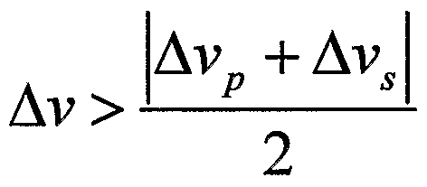


Priority Applications (5)
| Application Number | Priority Date | Filing Date | Title |
|---|---|---|---|
| EP03733376A EP1531355A4 (en) | 2002-06-11 | 2003-06-11 | SYSTEM AND METHOD FOR THE OPTICAL WAVELENGTH MULTIPLEX REGENERATION |
| JP2004511900A JPWO2003104886A1 (ja) | 2002-06-11 | 2003-06-11 | 波長分割多重光再生システム及び波長分割多重光再生方法 |
| US10/516,306 US8059966B2 (en) | 2002-06-11 | 2003-06-11 | Wavelength division multiplex optical regeneration system and wavelength division multiplex optical regeneration method |
| AU2003242289A AU2003242289A1 (en) | 2002-06-11 | 2003-06-11 | Wavelength divition multiplex optical regeneration system and wavelength division multiplex optical regeneration method |
| US13/269,886 US20120027343A1 (en) | 2002-06-11 | 2011-10-10 | Wavelength division multiplex optical regeneration system and wavelength division multiplex optical regeneration method |
Applications Claiming Priority (6)
| Application Number | Priority Date | Filing Date | Title |
|---|---|---|---|
| JP2002-170429 | 2002-06-11 | ||
| JP2002170429 | 2002-06-11 | ||
| JP2003-055645 | 2003-03-03 | ||
| JP2003055645 | 2003-03-03 | ||
| JP2003125659 | 2003-04-30 | ||
| JP2003-125659 | 2003-04-30 |
Related Child Applications (1)
| Application Number | Title | Priority Date | Filing Date |
|---|---|---|---|
| US13/269,886 Division US20120027343A1 (en) | 2002-06-11 | 2011-10-10 | Wavelength division multiplex optical regeneration system and wavelength division multiplex optical regeneration method |
Publications (1)
| Publication Number | Publication Date |
|---|---|
| WO2003104886A1 true WO2003104886A1 (ja) | 2003-12-18 |
Family
ID=29740545
Family Applications (1)
| Application Number | Title | Priority Date | Filing Date |
|---|---|---|---|
| PCT/JP2003/007433 Ceased WO2003104886A1 (ja) | 2002-06-01 | 2003-06-11 | 波長分割多重光再生システム及び波長分割多重光再生方法 |
Country Status (6)
| Country | Link |
|---|---|
| US (2) | US8059966B2 (ja) |
| EP (5) | EP2375595A1 (ja) |
| JP (3) | JPWO2003104886A1 (ja) |
| CN (1) | CN100454125C (ja) |
| AU (1) | AU2003242289A1 (ja) |
| WO (1) | WO2003104886A1 (ja) |
Cited By (12)
| Publication number | Priority date | Publication date | Assignee | Title |
|---|---|---|---|---|
| WO2006041103A1 (ja) * | 2004-10-12 | 2006-04-20 | Japan Science And Technology Agency | ロック検出装置及び光フェーズロックループシステム |
| JP2006251360A (ja) * | 2005-03-10 | 2006-09-21 | Sumitomo Electric Ind Ltd | 波長変換方法および波長変換器 |
| JP2007102157A (ja) * | 2005-09-06 | 2007-04-19 | Furukawa Electric Co Ltd:The | Cpfパルス成型器 |
| JP2007256323A (ja) * | 2006-03-20 | 2007-10-04 | Japan Science & Technology Agency | 光ad変換方法及び光ad変換器 |
| WO2008007615A1 (en) | 2006-07-11 | 2008-01-17 | Japan Science And Technology Agency | Synchronized optical signal generation device and synchronized optical signal generation method |
| JP2008028379A (ja) * | 2006-06-22 | 2008-02-07 | Fujifilm Corp | モードロックレーザ装置 |
| JP2010079246A (ja) * | 2008-09-01 | 2010-04-08 | Furukawa Electric Co Ltd:The | 光波形再生器および光波形再生方法 |
| WO2011125358A1 (ja) * | 2010-04-09 | 2011-10-13 | 浜松ホトニクス株式会社 | パルスファイバレーザ装置 |
| JP2012029334A (ja) * | 2011-10-27 | 2012-02-09 | Fujitsu Ltd | 光増幅装置および光受信装置 |
| CN101719800B (zh) * | 2008-10-09 | 2013-10-30 | 昂纳信息技术(深圳)有限公司 | 一种提高放大器中信号功率和噪声功率比值的方法和装置 |
| JP2014089254A (ja) * | 2012-10-29 | 2014-05-15 | Nippon Telegr & Teleph Corp <Ntt> | 位相感応型光増幅装置 |
| US12107380B1 (en) * | 2023-10-03 | 2024-10-01 | Vector Atomic, Inc. | Controlling soliton self-frequency shift |
Families Citing this family (41)
| Publication number | Priority date | Publication date | Assignee | Title |
|---|---|---|---|---|
| JP3570366B2 (ja) * | 2000-09-13 | 2004-09-29 | 日本電気株式会社 | アービタ回路及びそれに用いる出力セルのアービトレーション方法 |
| JP2005070610A (ja) * | 2003-08-27 | 2005-03-17 | Fujitsu Ltd | 多波長光源装置 |
| JP4304298B2 (ja) * | 2004-02-13 | 2009-07-29 | 日本電気株式会社 | 通信システム及びその同期方法 |
| US20070025660A1 (en) * | 2005-07-29 | 2007-02-01 | Su-Nam Lee | All-optical variable optical attenuator |
| JP4467557B2 (ja) * | 2006-12-25 | 2010-05-26 | 富士通株式会社 | 光スイッチング方法及び光スイッチ |
| JP5045170B2 (ja) * | 2007-03-19 | 2012-10-10 | 富士通株式会社 | 波形整形装置、光伝送システムおよび波形整形方法 |
| JP5304650B2 (ja) * | 2007-08-31 | 2013-10-02 | 富士通株式会社 | 光信号処理装置 |
| US8189257B2 (en) * | 2008-05-01 | 2012-05-29 | Massachusetts Institute Of Technology | Optimized cascaded raman fiber-based laser source for high efficiency mid-infrared spectral generation |
| CN101304284B (zh) * | 2008-06-20 | 2011-10-26 | 华中科技大学 | 一种多通道全光3r再生器 |
| JP5410534B2 (ja) | 2008-10-14 | 2014-02-05 | コーネル・ユニバーシティー | 位相シフトを入力波形に対して付与する装置 |
| WO2010091180A2 (en) * | 2009-02-05 | 2010-08-12 | Cornell University | High-speed optical sampling by temporal stretching using four-wave mixing |
| FI20095116A0 (fi) * | 2009-02-06 | 2009-02-06 | Luxdyne Oy | Vaihekohinan vähentäminen optisessa järjestelmässä |
| US8364042B2 (en) * | 2009-06-12 | 2013-01-29 | Kalpendu Shastri | Optical interconnection arrangement for high speed, high density communication systems |
| US8275263B1 (en) * | 2009-06-26 | 2012-09-25 | The Boeing Company | Multiplication of phase deviations |
| JP5648321B2 (ja) * | 2010-05-31 | 2015-01-07 | 富士通株式会社 | 波長変換装置、波長変換方法、及び、光分岐挿入装置 |
| US20120219285A1 (en) * | 2011-02-28 | 2012-08-30 | David Jimmy Dahan | In-band optical signal to noise ratio monitoring technique |
| US20120251111A1 (en) * | 2011-03-31 | 2012-10-04 | Nec Laboratories America, Inc. | Optoelectronic wavelength converter for polarization multiplexed optical signals |
| WO2012165163A1 (ja) * | 2011-06-03 | 2012-12-06 | 住友電気工業株式会社 | レーザ装置及びレーザ加工方法 |
| US20130087692A1 (en) * | 2011-10-05 | 2013-04-11 | Telcordia Technologies, Inc. | System and Method for Nonlinear Optical Devices |
| GB2496214B (en) * | 2011-11-01 | 2016-03-16 | Fianium Ltd | Amplifying optical device pumped or seeded with nonlinearly generated light |
| EP2637265B1 (en) | 2012-03-05 | 2018-08-29 | Menlo Systems GmbH | Laser with non-linear optical loop mirror |
| JP6119394B2 (ja) * | 2012-05-22 | 2017-04-26 | 沖電気工業株式会社 | 光増幅装置及び光増幅方法 |
| US8964798B2 (en) * | 2012-07-12 | 2015-02-24 | Kla-Tencor Corporation | Reducing the spectral bandwidth of lasers |
| WO2014120292A1 (en) * | 2012-10-19 | 2014-08-07 | Imra America, Inc. | Noise detection, diagnostics, and control of mode-locked lasers |
| KR101979249B1 (ko) * | 2012-12-21 | 2019-05-16 | 한국전자통신연구원 | 비팅 신호 모니터링 모듈, 그것을 포함하는 테라헤르츠파 발생 장치 및 광신호 모니터링 장치 |
| EP2846421A1 (en) | 2013-09-06 | 2015-03-11 | Menlo Systems GmbH | Laser with non-linear optical loop mirror |
| WO2016121090A1 (ja) * | 2015-01-30 | 2016-08-04 | ギガフォトン株式会社 | 固体レーザシステム |
| US9923634B2 (en) * | 2015-09-23 | 2018-03-20 | Fujitsu Limited | Harmonic generation and phase sensitive amplification using a bragg reflection waveguide |
| CN109565303B (zh) * | 2016-12-27 | 2020-12-08 | 华为技术有限公司 | 一种odu和odu发射功率的控制方法 |
| CN107505355A (zh) * | 2017-09-05 | 2017-12-22 | 北京工业大学 | 一维球形颗粒链非线性孤波传感器 |
| TWI638535B (zh) * | 2017-12-12 | 2018-10-11 | 美商光聯通訊有限公司 | Control device and method for optimizing transmission performance of optical communication system |
| CN110011732B (zh) * | 2018-01-05 | 2022-04-15 | 阿里巴巴集团控股有限公司 | 光纤传输系统和信号传输方法 |
| CN108347283B (zh) * | 2018-03-09 | 2023-09-29 | 中国科学院西安光学精密机械研究所 | 基于微腔光孤子晶体频梳的相干光通信系统 |
| RU189439U1 (ru) * | 2018-10-23 | 2019-05-22 | федеральное государственное бюджетное образовательное учреждение высшего образования "Ижевский государственный технический университет имени М.Т. Калашникова" | Источник импульсного лазерного излучения |
| CN109411995B (zh) * | 2018-12-10 | 2020-11-10 | 西南大学 | 一种中红外超快激光源装置 |
| CN109698458B (zh) * | 2019-01-24 | 2020-02-07 | 广东朗研科技有限公司 | 非线性环路滤波的Mamyshev型激光振荡器 |
| CN112260048B (zh) * | 2020-09-23 | 2022-09-16 | 武汉光谷航天三江激光产业技术研究院有限公司 | 一种激光波长周期性变化装置及方法 |
| CN118611633B (zh) * | 2024-05-24 | 2025-02-25 | 东莞理工学院 | 一种同轴结构的紧凑型微波脉冲压缩色散系统 |
| CN118713755B (zh) * | 2024-06-03 | 2025-11-04 | 华中科技大学 | 一种基于非线性傅里叶变换的孤子脉冲间距调控方法 |
| CN118984190B (zh) * | 2024-07-17 | 2025-11-25 | 电子科技大学 | 一种模分复用全光再生装置 |
| JP7813013B1 (ja) * | 2024-12-19 | 2026-02-12 | 浜松ホトニクス株式会社 | パルス光生成装置及びパルス光生成方法 |
Citations (3)
| Publication number | Priority date | Publication date | Assignee | Title |
|---|---|---|---|---|
| JPH11284261A (ja) * | 1998-03-27 | 1999-10-15 | Nippon Telegr & Teleph Corp <Ntt> | 低雑音光増幅装置 |
| JP2001008244A (ja) * | 1999-06-18 | 2001-01-12 | Nippon Telegr & Teleph Corp <Ntt> | 光クロスコネクト装置、光波長分割多重ネットワーク及び光波長分割多重方法 |
| EP1185007A2 (en) * | 2000-09-01 | 2002-03-06 | Fujitsu Limited | Method, device, and system for processing optical signals |
Family Cites Families (16)
| Publication number | Priority date | Publication date | Assignee | Title |
|---|---|---|---|---|
| GB2274952B (en) * | 1993-01-23 | 1996-12-04 | Northern Telecom Ltd | Optical soliton pulse transmission system |
| JPH09505154A (ja) * | 1993-11-12 | 1997-05-20 | ブリテイッシュ・テレコミュニケーションズ・パブリック・リミテッド・カンパニー | 光フィルタ |
| JPH08146474A (ja) * | 1994-11-22 | 1996-06-07 | Nippon Telegr & Teleph Corp <Ntt> | 光パルス生成方法及びその装置 |
| JPH08288902A (ja) * | 1995-04-14 | 1996-11-01 | Nippon Telegr & Teleph Corp <Ntt> | クロック再生装置 |
| US5715346A (en) * | 1995-12-15 | 1998-02-03 | Corning Incorporated | Large effective area single mode optical waveguide |
| US5600479A (en) * | 1995-12-22 | 1997-02-04 | Corning Incorporated | Method and apparatus for optical logic and switching functions |
| FR2758192B1 (fr) | 1997-01-06 | 1999-02-05 | Alsthom Cge Alcatel | Regenerateur de solitons a tres haut debit |
| FR2759830B1 (fr) | 1997-02-18 | 1999-03-26 | Alsthom Cge Alcatel | Regeneration optique pour des systemes de transmission a fibre optique a signaux non solitons |
| WO1999059025A1 (en) * | 1998-05-08 | 1999-11-18 | University Of Michigan | Soliton pulse transmission over waveguide fiber lengths |
| US6480656B1 (en) * | 1999-02-19 | 2002-11-12 | The Regents Of The University Of Michigan | Method and system for generating a broadband spectral continuum, method of making the system and pulse-generating system utilizing same |
| JP4460030B2 (ja) * | 1999-10-13 | 2010-05-12 | 古河電気工業株式会社 | 光ソリトン信号の波長制御方法 |
| JP3662463B2 (ja) * | 2000-02-14 | 2005-06-22 | 富士通株式会社 | 光信号を再生するための方法、装置及びシステム |
| US6587606B1 (en) * | 2000-10-20 | 2003-07-01 | Corning Incorporated | Waveguide fiber dispersion compensating regenerator |
| US6937782B2 (en) * | 2002-05-08 | 2005-08-30 | Massachusetts Institute Of Technology | Polarization-stabilized all-optical switch |
| JP4401626B2 (ja) * | 2002-07-05 | 2010-01-20 | 富士通株式会社 | 光信号を処理する方法及び装置 |
| WO2004049054A1 (ja) * | 2002-11-21 | 2004-06-10 | The Furukawa Electric Co., Ltd. | 光伝送システムにおける光源、波形整形器、光パルス列発生装置、及び 光再生システム |
-
2003
- 2003-06-11 CN CNB038135078A patent/CN100454125C/zh not_active Expired - Fee Related
- 2003-06-11 EP EP11158845A patent/EP2375595A1/en not_active Withdrawn
- 2003-06-11 EP EP03733376A patent/EP1531355A4/en not_active Withdrawn
- 2003-06-11 AU AU2003242289A patent/AU2003242289A1/en not_active Abandoned
- 2003-06-11 US US10/516,306 patent/US8059966B2/en not_active Expired - Fee Related
- 2003-06-11 WO PCT/JP2003/007433 patent/WO2003104886A1/ja not_active Ceased
- 2003-06-11 EP EP11158844A patent/EP2375594A1/en not_active Withdrawn
- 2003-06-11 JP JP2004511900A patent/JPWO2003104886A1/ja active Pending
- 2003-06-11 EP EP11158843A patent/EP2375593A1/en not_active Withdrawn
- 2003-06-11 EP EP11158841A patent/EP2375592A3/en not_active Withdrawn
-
2009
- 2009-10-13 JP JP2009236577A patent/JP2010022042A/ja active Pending
-
2011
- 2011-10-10 US US13/269,886 patent/US20120027343A1/en not_active Abandoned
-
2012
- 2012-10-29 JP JP2012238282A patent/JP2013057957A/ja not_active Withdrawn
Patent Citations (3)
| Publication number | Priority date | Publication date | Assignee | Title |
|---|---|---|---|---|
| JPH11284261A (ja) * | 1998-03-27 | 1999-10-15 | Nippon Telegr & Teleph Corp <Ntt> | 低雑音光増幅装置 |
| JP2001008244A (ja) * | 1999-06-18 | 2001-01-12 | Nippon Telegr & Teleph Corp <Ntt> | 光クロスコネクト装置、光波長分割多重ネットワーク及び光波長分割多重方法 |
| EP1185007A2 (en) * | 2000-09-01 | 2002-03-06 | Fujitsu Limited | Method, device, and system for processing optical signals |
Non-Patent Citations (2)
| Title |
|---|
| DANY B. ET AL.: "Full optimization of 40Gbit/s black-box optical regenerator for DWDM transoceanic transmissions", PROC. 27TH EUR. CONF. ON OPT. COMM., WE.P.45, 2001, pages 466 - 467, XP010589473 * |
| See also references of EP1531355A4 * |
Cited By (17)
| Publication number | Priority date | Publication date | Assignee | Title |
|---|---|---|---|---|
| US7715725B2 (en) | 2004-10-12 | 2010-05-11 | Japan Science And Technology Agency | Lock detector and optical phase-locked loop system |
| JP2006114996A (ja) * | 2004-10-12 | 2006-04-27 | Japan Science & Technology Agency | ロック検出装置及び光フェーズロックループシステム |
| WO2006041103A1 (ja) * | 2004-10-12 | 2006-04-20 | Japan Science And Technology Agency | ロック検出装置及び光フェーズロックループシステム |
| JP2006251360A (ja) * | 2005-03-10 | 2006-09-21 | Sumitomo Electric Ind Ltd | 波長変換方法および波長変換器 |
| JP2007102157A (ja) * | 2005-09-06 | 2007-04-19 | Furukawa Electric Co Ltd:The | Cpfパルス成型器 |
| JP2007256323A (ja) * | 2006-03-20 | 2007-10-04 | Japan Science & Technology Agency | 光ad変換方法及び光ad変換器 |
| JP2008028379A (ja) * | 2006-06-22 | 2008-02-07 | Fujifilm Corp | モードロックレーザ装置 |
| WO2008007615A1 (en) | 2006-07-11 | 2008-01-17 | Japan Science And Technology Agency | Synchronized optical signal generation device and synchronized optical signal generation method |
| US8494378B2 (en) | 2006-07-11 | 2013-07-23 | Japan Science And Technology Agency | Synchronous optical signal generating device and synchronous optical signal generating method |
| JP2010079246A (ja) * | 2008-09-01 | 2010-04-08 | Furukawa Electric Co Ltd:The | 光波形再生器および光波形再生方法 |
| CN101719800B (zh) * | 2008-10-09 | 2013-10-30 | 昂纳信息技术(深圳)有限公司 | 一种提高放大器中信号功率和噪声功率比值的方法和装置 |
| WO2011125358A1 (ja) * | 2010-04-09 | 2011-10-13 | 浜松ホトニクス株式会社 | パルスファイバレーザ装置 |
| JP2011222764A (ja) * | 2010-04-09 | 2011-11-04 | Hamamatsu Photonics Kk | パルスファイバレーザ装置 |
| US8724673B2 (en) | 2010-04-09 | 2014-05-13 | Hamamatsu Photonics K.K. | Pulse fiber laser device |
| JP2012029334A (ja) * | 2011-10-27 | 2012-02-09 | Fujitsu Ltd | 光増幅装置および光受信装置 |
| JP2014089254A (ja) * | 2012-10-29 | 2014-05-15 | Nippon Telegr & Teleph Corp <Ntt> | 位相感応型光増幅装置 |
| US12107380B1 (en) * | 2023-10-03 | 2024-10-01 | Vector Atomic, Inc. | Controlling soliton self-frequency shift |
Also Published As
| Publication number | Publication date |
|---|---|
| EP2375592A2 (en) | 2011-10-12 |
| EP2375594A1 (en) | 2011-10-12 |
| US20120027343A1 (en) | 2012-02-02 |
| EP2375595A1 (en) | 2011-10-12 |
| CN1659474A (zh) | 2005-08-24 |
| CN100454125C (zh) | 2009-01-21 |
| AU2003242289A1 (en) | 2003-12-22 |
| EP2375592A3 (en) | 2011-12-28 |
| EP2375593A1 (en) | 2011-10-12 |
| US20060204170A1 (en) | 2006-09-14 |
| EP1531355A4 (en) | 2008-08-13 |
| JP2013057957A (ja) | 2013-03-28 |
| JPWO2003104886A1 (ja) | 2005-10-13 |
| JP2010022042A (ja) | 2010-01-28 |
| US8059966B2 (en) | 2011-11-15 |
| EP1531355A1 (en) | 2005-05-18 |
Similar Documents
| Publication | Publication Date | Title |
|---|---|---|
| CN100454125C (zh) | 波形整形器 | |
| JP3920297B2 (ja) | 光スイッチおよび光スイッチを利用した光波形モニタ装置 | |
| JP5246217B2 (ja) | 光スイッチおよび光スイッチを利用した光波形モニタ装置 | |
| JP4401626B2 (ja) | 光信号を処理する方法及び装置 | |
| JP4472222B2 (ja) | 信号光を波形整形するための方法、装置及びシステム | |
| US8243363B2 (en) | Optical signal processing apparatus, optical receiving apparatus, and optical relay apparatus | |
| EP1152557B1 (en) | Method, device, and system for regenerating optical signals | |
| JP4574629B2 (ja) | 光スイッチおよび光スイッチを利用した光波形モニタ装置 | |
| US8351110B2 (en) | Optical-signal processing apparatus | |
| JP4629642B2 (ja) | 光スイッチおよび光スイッチを利用した光波形モニタ装置 | |
| CN100353254C (zh) | 光开关和利用光开关的光波形监测装置 | |
| Kuksenkov et al. | Nonlinear fibre devices operating on multiple WDM channels | |
| Sharif et al. | All-optical pulsewidth-tunable wavelength conversion of return-to-zero differential phase-shift keying signal | |
| Ismail et al. | Wide range operation of an all-optical NRZ-DPSK-to-RZ-DPSK regenerative waveform–wavelength conversion with flexible width-tunability | |
| Galili et al. | Low-penalty Raman-assisted XPM wavelength conversion at 320 Gb/s | |
| Marembert | Investigations on ultrafast fiber based optical gates | |
| NGUYEN | Multiwavelength Optical Signal Processing for Reconfigurable Fiber-Optic Communication Systems | |
| Yu | Dispersive and nonlinear effects in high-speed reconfigurable WDM optical fiber communication systems | |
| Matsuura et al. | All-optical pulsewidth-tunable wavelength conversion of return-to-zero differential phase-shift keying signal | |
| Set | Dispersion compensation in high bit rate transmission systems using midspan spectral inversion | |
| Yamamoto | Study on High-Speed and Large-Capacity Signal Transmission Technology | |
| JP2004151747A (ja) | 波形整形のための装置 |
Legal Events
| Date | Code | Title | Description |
|---|---|---|---|
| AK | Designated states |
Kind code of ref document: A1 Designated state(s): AE AG AL AM AT AU AZ BA BB BG BR BY BZ CA CH CN CO CR CU CZ DE DK DM DZ EC EE ES FI GB GD GE GH GM HR HU ID IL IN IS JP KE KG KP KR KZ LC LK LR LS LT LU LV MA MD MG MK MN MW MX MZ NI NO NZ OM PH PL PT RO RU SC SD SE SG SK SL TJ TM TN TR TT TZ UA UG US UZ VC VN YU ZA ZM ZW |
|
| AL | Designated countries for regional patents |
Kind code of ref document: A1 Designated state(s): GH GM KE LS MW MZ SD SL SZ TZ UG ZM ZW AM AZ BY KG KZ MD RU TJ TM AT BE BG CH CY CZ DE DK EE ES FI FR GB GR HU IE IT LU MC NL PT RO SE SI SK TR BF BJ CF CG CI CM GA GN GQ GW ML MR NE SN TD TG |
|
| 121 | Ep: the epo has been informed by wipo that ep was designated in this application | ||
| WWE | Wipo information: entry into national phase |
Ref document number: 2004511900 Country of ref document: JP |
|
| WWE | Wipo information: entry into national phase |
Ref document number: 20038135078 Country of ref document: CN |
|
| WWE | Wipo information: entry into national phase |
Ref document number: 2003733376 Country of ref document: EP |
|
| WWP | Wipo information: published in national office |
Ref document number: 2003733376 Country of ref document: EP |
|
| WWE | Wipo information: entry into national phase |
Ref document number: 10516306 Country of ref document: US |
|
| WWP | Wipo information: published in national office |
Ref document number: 10516306 Country of ref document: US |