WO2004065520A1 - 発光素子、それに用いる縮合多環系化合物及びその製造方法 - Google Patents
発光素子、それに用いる縮合多環系化合物及びその製造方法 Download PDFInfo
- Publication number
- WO2004065520A1 WO2004065520A1 PCT/JP2004/000306 JP2004000306W WO2004065520A1 WO 2004065520 A1 WO2004065520 A1 WO 2004065520A1 JP 2004000306 W JP2004000306 W JP 2004000306W WO 2004065520 A1 WO2004065520 A1 WO 2004065520A1
- Authority
- WO
- WIPO (PCT)
- Prior art keywords
- group
- compound
- light
- aromatic
- halogen atom
- Prior art date
- Legal status (The legal status is an assumption and is not a legal conclusion. Google has not performed a legal analysis and makes no representation as to the accuracy of the status listed.)
- Ceased
Links
Classifications
-
- C—CHEMISTRY; METALLURGY
- C09—DYES; PAINTS; POLISHES; NATURAL RESINS; ADHESIVES; COMPOSITIONS NOT OTHERWISE PROVIDED FOR; APPLICATIONS OF MATERIALS NOT OTHERWISE PROVIDED FOR
- C09K—MATERIALS FOR MISCELLANEOUS APPLICATIONS, NOT PROVIDED FOR ELSEWHERE
- C09K11/00—Luminescent materials, e.g. electroluminescent or chemiluminescent
- C09K11/06—Luminescent materials, e.g. electroluminescent or chemiluminescent containing organic luminescent materials
-
- C—CHEMISTRY; METALLURGY
- C07—ORGANIC CHEMISTRY
- C07D—HETEROCYCLIC COMPOUNDS
- C07D471/00—Heterocyclic compounds containing nitrogen atoms as the only ring hetero atoms in the condensed system, at least one ring being a six-membered ring with one nitrogen atom, not provided for by groups C07D451/00 - C07D463/00
- C07D471/02—Heterocyclic compounds containing nitrogen atoms as the only ring hetero atoms in the condensed system, at least one ring being a six-membered ring with one nitrogen atom, not provided for by groups C07D451/00 - C07D463/00 in which the condensed system contains two hetero rings
- C07D471/06—Peri-condensed systems
-
- C—CHEMISTRY; METALLURGY
- C07—ORGANIC CHEMISTRY
- C07D—HETEROCYCLIC COMPOUNDS
- C07D491/00—Heterocyclic compounds containing in the condensed ring system both one or more rings having oxygen atoms as the only ring hetero atoms and one or more rings having nitrogen atoms as the only ring hetero atoms, not provided for by groups C07D451/00 - C07D459/00, C07D463/00, C07D477/00 or C07D489/00
- C07D491/02—Heterocyclic compounds containing in the condensed ring system both one or more rings having oxygen atoms as the only ring hetero atoms and one or more rings having nitrogen atoms as the only ring hetero atoms, not provided for by groups C07D451/00 - C07D459/00, C07D463/00, C07D477/00 or C07D489/00 in which the condensed system contains two hetero rings
- C07D491/06—Peri-condensed systems
-
- C—CHEMISTRY; METALLURGY
- C07—ORGANIC CHEMISTRY
- C07D—HETEROCYCLIC COMPOUNDS
- C07D493/00—Heterocyclic compounds containing oxygen atoms as the only ring hetero atoms in the condensed system
- C07D493/02—Heterocyclic compounds containing oxygen atoms as the only ring hetero atoms in the condensed system in which the condensed system contains two hetero rings
- C07D493/06—Peri-condensed systems
-
- C—CHEMISTRY; METALLURGY
- C07—ORGANIC CHEMISTRY
- C07D—HETEROCYCLIC COMPOUNDS
- C07D495/00—Heterocyclic compounds containing in the condensed system at least one hetero ring having sulfur atoms as the only ring hetero atoms
- C07D495/02—Heterocyclic compounds containing in the condensed system at least one hetero ring having sulfur atoms as the only ring hetero atoms in which the condensed system contains two hetero rings
- C07D495/06—Peri-condensed systems
-
- C—CHEMISTRY; METALLURGY
- C07—ORGANIC CHEMISTRY
- C07D—HETEROCYCLIC COMPOUNDS
- C07D517/00—Heterocyclic compounds containing in the condensed system at least one hetero ring having selenium, tellurium, or halogen atoms as ring hetero atoms
- C07D517/02—Heterocyclic compounds containing in the condensed system at least one hetero ring having selenium, tellurium, or halogen atoms as ring hetero atoms in which the condensed system contains two hetero rings
- C07D517/06—Peri-condensed systems
-
- C—CHEMISTRY; METALLURGY
- C07—ORGANIC CHEMISTRY
- C07D—HETEROCYCLIC COMPOUNDS
- C07D517/00—Heterocyclic compounds containing in the condensed system at least one hetero ring having selenium, tellurium, or halogen atoms as ring hetero atoms
- C07D517/02—Heterocyclic compounds containing in the condensed system at least one hetero ring having selenium, tellurium, or halogen atoms as ring hetero atoms in which the condensed system contains two hetero rings
- C07D517/08—Bridged systems
-
- C—CHEMISTRY; METALLURGY
- C09—DYES; PAINTS; POLISHES; NATURAL RESINS; ADHESIVES; COMPOSITIONS NOT OTHERWISE PROVIDED FOR; APPLICATIONS OF MATERIALS NOT OTHERWISE PROVIDED FOR
- C09B—ORGANIC DYES OR CLOSELY-RELATED COMPOUNDS FOR PRODUCING DYES, e.g. PIGMENTS; MORDANTS; LAKES
- C09B1/00—Dyes with anthracene nucleus not condensed with any other ring
- C09B1/50—Amino-hydroxy-anthraquinones; Ethers and esters thereof
- C09B1/54—Amino-hydroxy-anthraquinones; Ethers and esters thereof etherified
- C09B1/547—Anthraquinones with aromatic ether groups
-
- C—CHEMISTRY; METALLURGY
- C09—DYES; PAINTS; POLISHES; NATURAL RESINS; ADHESIVES; COMPOSITIONS NOT OTHERWISE PROVIDED FOR; APPLICATIONS OF MATERIALS NOT OTHERWISE PROVIDED FOR
- C09B—ORGANIC DYES OR CLOSELY-RELATED COMPOUNDS FOR PRODUCING DYES, e.g. PIGMENTS; MORDANTS; LAKES
- C09B1/00—Dyes with anthracene nucleus not condensed with any other ring
- C09B1/56—Mercapto-anthraquinones
- C09B1/58—Mercapto-anthraquinones with mercapto groups substituted by aliphatic, cycloaliphatic, araliphatic or aryl radicals
- C09B1/585—Mercapto-anthraquinones with mercapto groups substituted by aliphatic, cycloaliphatic, araliphatic or aryl radicals substituted by aryl radicals
-
- C—CHEMISTRY; METALLURGY
- C09—DYES; PAINTS; POLISHES; NATURAL RESINS; ADHESIVES; COMPOSITIONS NOT OTHERWISE PROVIDED FOR; APPLICATIONS OF MATERIALS NOT OTHERWISE PROVIDED FOR
- C09B—ORGANIC DYES OR CLOSELY-RELATED COMPOUNDS FOR PRODUCING DYES, e.g. PIGMENTS; MORDANTS; LAKES
- C09B1/00—Dyes with anthracene nucleus not condensed with any other ring
- C09B1/56—Mercapto-anthraquinones
- C09B1/58—Mercapto-anthraquinones with mercapto groups substituted by aliphatic, cycloaliphatic, araliphatic or aryl radicals
- C09B1/60—Mercapto-anthraquinones with mercapto groups substituted by aliphatic, cycloaliphatic, araliphatic or aryl radicals substituted by aliphatic, cycloaliphatic or araliphatic radicals
-
- C—CHEMISTRY; METALLURGY
- C09—DYES; PAINTS; POLISHES; NATURAL RESINS; ADHESIVES; COMPOSITIONS NOT OTHERWISE PROVIDED FOR; APPLICATIONS OF MATERIALS NOT OTHERWISE PROVIDED FOR
- C09B—ORGANIC DYES OR CLOSELY-RELATED COMPOUNDS FOR PRODUCING DYES, e.g. PIGMENTS; MORDANTS; LAKES
- C09B5/00—Dyes with an anthracene nucleus condensed with one or more heterocyclic rings with or without carbocyclic rings
- C09B5/02—Dyes with an anthracene nucleus condensed with one or more heterocyclic rings with or without carbocyclic rings the heterocyclic ring being only condensed in peri position
- C09B5/18—Coeroxene; Coerthiene; Coeramidene; Derivatives thereof
-
- H—ELECTRICITY
- H05—ELECTRIC TECHNIQUES NOT OTHERWISE PROVIDED FOR
- H05B—ELECTRIC HEATING; ELECTRIC LIGHT SOURCES NOT OTHERWISE PROVIDED FOR; CIRCUIT ARRANGEMENTS FOR ELECTRIC LIGHT SOURCES, IN GENERAL
- H05B33/00—Electroluminescent light sources
- H05B33/12—Light sources with substantially two-dimensional [2D] radiating surfaces
- H05B33/14—Light sources with substantially two-dimensional [2D] radiating surfaces characterised by the chemical or physical composition or the arrangement of the electroluminescent material, or by the simultaneous addition of the electroluminescent material in or onto the light source
-
- H—ELECTRICITY
- H10—SEMICONDUCTOR DEVICES; ELECTRIC SOLID-STATE DEVICES NOT OTHERWISE PROVIDED FOR
- H10K—ORGANIC ELECTRIC SOLID-STATE DEVICES
- H10K85/00—Organic materials used in the body or electrodes of devices covered by this subclass
- H10K85/60—Organic compounds having low molecular weight
- H10K85/649—Aromatic compounds comprising a hetero atom
- H10K85/657—Polycyclic condensed heteroaromatic hydrocarbons
- H10K85/6574—Polycyclic condensed heteroaromatic hydrocarbons comprising only oxygen in the heteroaromatic polycondensed ring system, e.g. cumarine dyes
-
- H—ELECTRICITY
- H10—SEMICONDUCTOR DEVICES; ELECTRIC SOLID-STATE DEVICES NOT OTHERWISE PROVIDED FOR
- H10K—ORGANIC ELECTRIC SOLID-STATE DEVICES
- H10K85/00—Organic materials used in the body or electrodes of devices covered by this subclass
- H10K85/60—Organic compounds having low molecular weight
- H10K85/649—Aromatic compounds comprising a hetero atom
- H10K85/657—Polycyclic condensed heteroaromatic hydrocarbons
- H10K85/6576—Polycyclic condensed heteroaromatic hydrocarbons comprising only sulfur in the heteroaromatic polycondensed ring system, e.g. benzothiophene
-
- C—CHEMISTRY; METALLURGY
- C09—DYES; PAINTS; POLISHES; NATURAL RESINS; ADHESIVES; COMPOSITIONS NOT OTHERWISE PROVIDED FOR; APPLICATIONS OF MATERIALS NOT OTHERWISE PROVIDED FOR
- C09K—MATERIALS FOR MISCELLANEOUS APPLICATIONS, NOT PROVIDED FOR ELSEWHERE
- C09K2211/00—Chemical nature of organic luminescent or tenebrescent compounds
- C09K2211/10—Non-macromolecular compounds
- C09K2211/1018—Heterocyclic compounds
-
- H—ELECTRICITY
- H10—SEMICONDUCTOR DEVICES; ELECTRIC SOLID-STATE DEVICES NOT OTHERWISE PROVIDED FOR
- H10K—ORGANIC ELECTRIC SOLID-STATE DEVICES
- H10K85/00—Organic materials used in the body or electrodes of devices covered by this subclass
- H10K85/60—Organic compounds having low molecular weight
- H10K85/615—Polycyclic condensed aromatic hydrocarbons, e.g. anthracene
-
- Y—GENERAL TAGGING OF NEW TECHNOLOGICAL DEVELOPMENTS; GENERAL TAGGING OF CROSS-SECTIONAL TECHNOLOGIES SPANNING OVER SEVERAL SECTIONS OF THE IPC; TECHNICAL SUBJECTS COVERED BY FORMER USPC CROSS-REFERENCE ART COLLECTIONS [XRACs] AND DIGESTS
- Y02—TECHNOLOGIES OR APPLICATIONS FOR MITIGATION OR ADAPTATION AGAINST CLIMATE CHANGE
- Y02B—CLIMATE CHANGE MITIGATION TECHNOLOGIES RELATED TO BUILDINGS, e.g. HOUSING, HOUSE APPLIANCES OR RELATED END-USER APPLICATIONS
- Y02B20/00—Energy efficient lighting technologies, e.g. halogen lamps or gas discharge lamps
-
- Y—GENERAL TAGGING OF NEW TECHNOLOGICAL DEVELOPMENTS; GENERAL TAGGING OF CROSS-SECTIONAL TECHNOLOGIES SPANNING OVER SEVERAL SECTIONS OF THE IPC; TECHNICAL SUBJECTS COVERED BY FORMER USPC CROSS-REFERENCE ART COLLECTIONS [XRACs] AND DIGESTS
- Y10—TECHNICAL SUBJECTS COVERED BY FORMER USPC
- Y10S—TECHNICAL SUBJECTS COVERED BY FORMER USPC CROSS-REFERENCE ART COLLECTIONS [XRACs] AND DIGESTS
- Y10S428/00—Stock material or miscellaneous articles
- Y10S428/917—Electroluminescent
Definitions
- the present invention relates to a light emitting device, a condensed polycyclic compound used therefor, and a method for producing the same.
- the present invention relates to a light-emitting element having a thin film of an organic compound and emitting light when energized, a condensed polycyclic compound used for the light-emitting element, and a method for producing the same.
- the light emitting device can be used in the fields of display devices, flat panel displays, backlights, lighting, interiors, signs, signboards, electrophotographic machines, optical signal generators, and the like. Background technology ''
- organic electronic components include organic transistors as organic electronic devices, organic semiconductor lasers, organic solar cells, and organic EL devices.
- organic EL (light emitting) elements are expected as high-quality display elements, and practical use has begun. In particular, it features low power consumption, ultra-thin film, high-luminance light emission, and self-emission with high visibility.It is actively researched and applied for next-generation displays, flat light sources, and light-emitting elements. And
- the configuration of an organic EL element using an organic material is such that an organic phosphor thin film (light emitting layer) and a hole transporting layer are laminated between a metal electrode as a cathode and a translucent transparent electrode as an anode.
- Two-layer structure (single-hetero structure), and a three-tank structure (double heterostructure) in which an electron transport layer, luminescent and hole transport layers are laminated between a metal electrode and a transparent electrode. ) are known.
- the hole transport layer has a function of injecting and transporting holes from the anode and a function of blocking electrons
- the electron transporting layer has a function of injecting and transporting electrons from the cathode. are doing.
- a multilayer structure having a hole injection layer, an electron injection layer, a hole blocking layer, and the like appropriately arranged has been developed. These have a structure in which the functions are further separated from those of the two-layer or three-layer structure, and have the function of facilitating the injection of holes and electrons, and the function of blocking leaking electrons and holes, respectively. Its purpose is to enhance the brightness, improve the brightness by efficient recombination of electrons and holes, improve the durability, extend the life, and reduce the power consumption by reducing the applied voltage. 'In these light-emitting devices using a thin film of an organic material, a substrate made of glass, plastic or an appropriate material is disposed outside the transparent electrode.
- the exciton emits light in the process of radiation deactivation, and this light is emitted outside through the transparent electrode and the glass substrate.
- This device is characterized by its thinness, high-brightness light emission under a low driving voltage, multicolor light emission by selecting a material to emit light, and the like.
- a typical structure of an organic layered thin-film light-emitting device presented by a research group of the First Man Kodak Company is a diamine compound with a hole-transporting property on an ITO glass substrate, and a tris (8-quinolinolato) that is both a light-emitting layer and an electron-transporting layer.
- An aluminum complex and Mg: Ag (alloy) as a cathode are sequentially provided.
- red light emitting material examples include a perylene-based material such as bis (diisopropylphenyl) perylene, a porphyrin-based material, a europium complex, and a julolidine-substituted styryl compound (for example, see JP-A-2001-43974).
- a small amount of a red fluorescent compound is contained as a dopant in a host material to change the emission color (emission wavelength) to a desired color.
- quinolinol derivatives including tris (8-quinolinolato) aluminum complex, bis (10-benzoquinolinolato) beryllium complex, diarylbutadiene derivative, stilbene derivative, benzoxazole derivative Benzothiazole derivatives, perinone derivatives and the like.
- these luminescent materials used in the prior art have low luminous efficiency and do not provide high luminance, and do not emit light with a poor color purity and orange tint even when doped.
- the major problem was that many of them had low durability and short element life, and few had both color purity and brightness. There is also a situation where the efficiency of orange light emitting elements is not sufficient.
- such a light-emitting element generally uses a transparent electrode provided on a glass or polymer substrate as an anode, and a hole injection layer, a hole transport layer, and the like are usually formed thereon.
- I have.
- the work function of these transparent electrodes, such as ITO generally has a large difference from the hole transport layer, and the energy level does not match.
- the adhesion between the ITO and the hole transport layer is poor, so that the work function of the hole transport layer is poor. Crystallisation occurred, the applied voltage was increased, the efficiency was reduced, and instability at the time of driving was caused.
- a method of forming a transparent electrode such as an I T ⁇ at the end, such as a top emission structure has also been studied, but similarly, there has been a problem such as a decrease in efficiency. '
- phthalocyanine derivatives are disclosed in JP-A-57-51781, JP-A-63-295695 and JP-A-8-1999. It is described in No. 161 publication.
- thiophene derivatives see JP-A-5-94877
- aromatic amine derivatives see JP-A-8-26445
- hydrazone derivatives see JP-A-4-1320.
- Low molecular weight compounds such as polythiophene, polyaniline, polychenylenevinylene, and polyphenylenevinylene (see Japanese Patent Application Laid-Open No. 4-145192) have been reported. .
- condensed polycyclic compound described in the present invention for example, E. Clar, W. Kelly, DGStewart, JW Wright, J. Chem. So, (1956), 2652; Tokita, Arai, Ooka, Nishi 198, (5), 876; J. Photopolym. Sci. Technol., 11, 41 (1998); Tokita, Arai, Toya, Nishi, The Chemical Society of Japan, 1988, (5), 814; West Japan Chemical Society, 1988, (1), 97; Mol. Cryst. Liq. Cryst., 1994, Vol. 246, 119; R. SCHMIDT, W. DREWS, H. -D.
- the present invention provides a light-emitting element capable of emitting orange to red light with high luminous efficiency, a light-emitting material (host material and doping material) for a white light-emitting element, and light-emitting capable of emitting light of high luminance and high color purity.
- a light-emitting element according to the present invention can be driven at a low voltage, has high luminous efficiency, and has practical stability and long life.
- the novel condensed polycyclic compound provided by the present invention is useful as an organic electronic material, particularly as an organic EL material. '
- X 2 , X 3 and X 4 each independently represent an oxygen atom, a sulfur atom, a selenium atom, a tellurium atom or NR 29.
- R 29 may have a hydrogen atom or a substituent.
- a light emitting element comprising a compound having a basic skeleton represented by an aliphatic hydrocarbon residue or an aromatic residue which may have a substituent.
- the compound having the basic skeleton represented by the general formula (1) or (2) is represented by the following general formula (3) or (4)
- halogen atom is a bromine atom or a fluorine atom.
- X 2 of the compound represented by the general formula (3) are each independently an oxygen atom or a sulfur atom; is H, F, CH 3 , Ph or CF 3 ;
- R 2 is H, C3 ⁇ 4, C 2 H 5, t one C 4 H 9, Cy, P h, MPh, Np, Th, Py, ⁇ _CH 3, OPh, F, C l , B r, I, CN, N (CH 3) 2, CHO, C_ ⁇ _ ⁇ _H, C_ ⁇ _OCH 3, C_ ⁇ _ ⁇ _Ph, COP and h, or CF 3;
- R 3 is H, CH 3, C 2 H 5, t one C 4 H 9, ⁇ _CH 3, OPh, N0 2 , OH, F, CF 3, C a 2 F 5, or Ph;
- R 4 is H, CH 3, C 2 H 5, t one C 4 H 9, Cy, Ph , MPh, Np, Th, P y, ⁇ CH 3, OPh, F, C l, B r
- R 8 is H, F, CH 3 , Ph or CF 3 ;
- R 9 is H, CH 3 , C 2 H 5 , t—C 4 H 9 , Cy, Ph, MPh, Np, Th, Py, ⁇ CH 3 , ⁇ Ph, F, Cl, Br, I, CN, N (CH 3 ) 2 , CHO, CO ⁇ H, CO OCH 3 , C ⁇ Ph, C ⁇ Ph or CF 3 ; .
- the light-emitting device according to any one of the above items 1 to 14, wherein the light-emitting device emits white light by using a blue to green light-emitting material in combination.
- the light-emitting device according to any one of the above items 1 to 16, characterized in that the display is a display that displays in a matrix, Z, or segment system.
- R 3 to R 43 are each independently a hydrogen atom; a halogen atom; an alkyl group which may have an aromatic residue, an aromatic oxy group, an alkyloxy group or a halogen atom as a substituent; An aromatic residue, an aromatic oxy group, an alkyl group, an alkyloxy group or an aromatic residue which may have a halogen atom as a substituent, and at least one of R 3 to R 43 is Substituted with an aromatic residue, an aromatic oxy group, an alkyl group, an alkyloxy group or a halogen atom Or an aromatic residue or a halogen atom.
- R 3Q to R 43 may be linked with each other to form a ring which may have a substituent, provided that R 3Q to R 43 are R 3 .
- R 3Q to R 43 are R 3 .
- R 32 and R 33 and R 39 and R 4. are linked to form an unsubstituted benzene ring, and R 3 .
- To R 43 except for those not forming a ring are all hydrogen atoms ⁇ )
- R 3. The above-mentioned item 18, wherein at least two of R 43 to R 43 are an aromatic residue, an aromatic oxy group, an alkyl group, an alkyloxy group or an aromatic residue or a halogen atom which may have a halogen atom as a substituent.
- R 42 'R 43 is a hydrogen atom; ⁇ .
- R 7 is a hydrogen atom, a halogen atom, a C1-C4 alkyl group;
- R 31, R 33, R 3S , R 4. Is hydrogen atom, halogen atom, aromatic residue, phenyl group, C
- R 44 to R 57 each independently represent a hydrogen atom; a halogen atom; an aromatic residue, an aromatic oxy group, an alkyloxy group, or an alkyl group optionally substituted with a halogen atom; A residue, an aromatic oxy group, an alkyl group, an alkyloxy group, or an aromatic residue which may be substituted with a halogen atom, and at least one of R 44 to R 57 is an aromatic residue, An aromatic oxy group, an alkyloxy group, or an alkyl group optionally substituted with a halogen atom; an aromatic residue, an aromatic oxy group, an alkyl group, an aromatic group optionally substituted with a halogen atom, Or a halogen atom.
- R 44 to R 57 may be linked to each other to form a ring which may have a substituent.
- X 3 and X 4 each independently represent an oxygen atom, a sulfur atom, a selenium atom, a tellurium atom or NR 72.
- R 72 is a hydrogen atom, an alkyl group, an alkyloxy group, an aromatic residue as a substituent, Represents an aliphatic hydrocarbon residue or an aromatic residue which may have an aromatic oxy group or a halogen atom, wherein R 5S to R 71 are a hydrogen atom; a halogen atom; an aromatic residue; Group, Arukiruokishi group or an alkyl group which may be substituted with halogen atoms; represents an aromatic residue, an aromatic Okishi group, an alkyl group, an aromatic Zokuzanmoto be substituted with Arukiruokishi group or a halogen atom, and R 58 ⁇ : At least one of 71 is an octylogen atom; an aromatic residue, an aromatic oxy group, an alkyloxy group or an al
- sulfonic acid compound is sulfuric acid, an alkyl sulfonic acid which may have a substituent, or an aromatic sulfonic acid which may have a substituent.
- FIG. 1 and 2 are schematic cross-sectional views showing examples of the layer structure of the light emitting device of the present invention. -Best mode for carrying out the invention
- the present invention relates to an element which emits light by electric energy in which an organic thin film including a hole transporting layer and an electron transporting layer is formed between an anode and a cathode, wherein at least the compound represented by the general formula (1) or (2) Characterized by containing a compound having a basic skeleton described below.
- X 2, X 3 and X 4 each independently represent an oxygen atom, sulfur atom, selenium atom, a tellurium atom or NR 29.
- R 29 represents a hydrogen atom, an aliphatic hydrocarbon residue which may have a substituent, or an aromatic residue which may have a substituent.
- the compounds having the basic skeleton represented by the general formulas (1) and (2) may have a substituent, and the substituents may be combined with each other to form a ring.
- Examples of the compound having the basic skeleton represented by the general formula (1) include a compound represented by the following general formula (3), and a compound having the basic skeleton represented by the general formula (2) ' Examples thereof include a compound represented by the general formula (4).
- Formula (3) and (4) in X 2, X 3 and X 4 each independently represent an oxygen atom, sulfur atom, selenium atom, a tellurium atom or NR 29, may each be the same or different.
- R 29 represents a hydrogen atom, an aliphatic hydrocarbon residue which may have a substituent, or an aromatic residue which may have a substituent.
- the aliphatic hydrocarbon residue optionally having a substituent or the aromatic residue optionally having a substituent represented by R 29 may have a substituent described in 1 to 28 described below.
- ⁇ ⁇ ⁇ 2 8 each independently represent a hydrogen atom or a substituent, the substituents may form a optionally substituted by linking group each other in proximity to each other rings.
- an aliphatic hydrocarbon residue which may have a substituent an aromatic residue which may have a substituent, a cyano group, a nitro group, an acyl group, a halogen atom, a hydroxyl group, substituted or unsubstituted
- an amino group, an alkoxyl group, an aromatic oxy group which may have a substituent and the like More preferred are an aliphatic hydrocarbon residue which may have a substituent, an aromatic residue which may have a substituent, a nitro group, a halogen atom, a substituted or unsubstituted amino group, and an alkoxy group.
- an aliphatic hydrocarbon residue which may have a substituent an aromatic residue which may have a substituent, and an octagonal atom are more preferable. Most preferably, it is an aromatic residue which may have a substituent.
- aromatic groups a phenyl group which may have a substituent is preferable.
- an aromatic residue that may have a plurality substituents, in particular compounds when good Fuweniru group which may have a substituent is more preferable.
- Examples of the aliphatic hydrocarbon residue which may have a substituent include a saturated or unsaturated linear, branched or cyclic aliphatic hydrocarbon residue which may have a substituent. ⁇ 20 is preferred.
- Examples of the saturated or unsaturated linear or branched aliphatic hydrocarbon residue include a methyl group, an ethyl group, a propyl group, an isopropyl group, an ⁇ -butyl group, an iso-butyl group, an aryl group and a t-butyl group.
- n-pentyl n-hexyl, n-octyl, n-decyl, n-dodecyl, n-stearyl, n-butenyl and the like.
- the cyclic aliphatic hydrocarbon residue include a cycloalkyl group having 3 to 12 carbon atoms, such as a cyclohexyl group, a cyclopentyl group, an adamantyl group, and a norpolnyl group. These aliphatic hydrocarbon residues may be further substituted with the above substituents (excluding the alkyl group).
- the preferred aliphatic hydrocarbon residue is an alkyl group having 1 to 6 carbon atoms which may have a substituent.
- substituents on these aliphatic hydrocarbon residues are, for example, halogen atoms, preferably chloro atoms, bromine atoms, fluorine atoms, particularly preferably fluorine atoms, or aromatic groups which may have a substituent, preferably Is a phenyl group which may have a substituent.
- the aromatic residue which may have a substituent include a 5- or 6-membered aromatic residue which may contain 1 to 3 substituted or unsubstituted hetero atoms, or a plurality of the 5- or 6-membered ring.
- aromatic residues linked as a condensed ring examples include an oxygen atom, a nitrogen atom, and a sulfur atom, and a nitrogen atom is preferable.
- aromatic hydrocarbon residues such as phenyl, naphthyl, anthryl, phenanthryl, pyrenyl, benzopyrenyl, pyridyl, pyrazyl, pyrazyl, pyrimidyl, quinolyl, isoquinolyl, pyrrolyl, indolenyl And aromatic heterocyclic residues such as a group, imidazolyl group, carpazolyl group, chenyl group and furyl group, and those having a substituent such as benzoquinolyl group, anthraquinolyl group, pyranyl group and pyridonyl group.
- Preferable examples include a phenyl group, a naphthyl group, a pyridyl group, and a phenyl group. Particularly, a phenyl group and a naphthyl group are preferable. “Aromatic” in the aromatic oxy group and the like is used in the same meaning as the aromatic residue.
- acyl group examples include an alkylcarbonyl group having 1 to 10 carbon atoms and an arylcarbonyl group, and preferably an alkylcarbonyl group having 1 to 4 carbon atoms, specifically, an acetyl group, a propionyl group, and the like. No. .
- halogen atom examples include atoms such as fluorine, chlorine, bromine, and iodine. Preferred are fluorine, chlorine and bromine atoms, and more preferred are fluorine and bromine atoms.
- substituted or unsubstituted amino group include an amino group, a mono- or di-alkylamino group, a mono- or di-aromatic amino group, and the like. Or a mono- or di-C 1 -C 6 alkyl group which may have a substituent such as a benzylamino group, and the substituent on the alkyl group is the above-mentioned substitution on the aliphatic hydrocarbon residue. And a phenyl group or a barogen atom. ,
- alkoxyl group examples include a (C 1 -C 10) alkoxyl group, and a (C 1 -C 4) alkoxyl group such as a methoxy group, an ethoxy group, a propoxy group, and a butoxy group are preferable.
- alkoxyalkyl group examples include a (C1-C10) alkoxy (C1-C10) alkyl group.
- Examples of the aromatic oxy group include a C 1 to C 20 aromatic oxy group which may contain 1 to 3 hetero atoms.
- Examples of the aromatic oxy group include (C 6 to C 4) such as a phenoxy group and a naphthyloxy group.
- Examples of the alkoxycarbonyl group include a (C1-C10) alkoxycarbonyl group.
- Examples of the aromatic oxycarbonyl group which may have a substituent include a phenoxycarbonyl group which may be substituted with a halogen atom or the like.
- the Contact Keru substituents aromatic residue which may have those aliphatic hydrocarbon residue or a substituent having a substituent is not particularly limited mentioned in the previous 1 ⁇ to 1 28
- aromatic groups more preferably a phenyl group which may have a substituent, and an octane atom.
- Ri R and R 29 are summarized as follows: an aliphatic hydrocarbon residue which may have a substituent; an aromatic residue which may have a substituent; Atom.
- an aliphatic hydrocarbon residue which may have a substituent an unsubstituted C 1 -C 6 lower alkyl group or a halogen-substituted or alkoxy-substituted lower alkyl group is preferable.
- Examples of the aromatic residue which may have a substituent include a phenyl group, a biphenyl group, a naphthyl group, a pyridino group, a chenyl group, a furyl group, and an aliphatic hydrocarbon residue or an aromatic residue as a substituent. These groups having at least one group selected from the group consisting of and a halogen atom are preferred.
- the aliphatic hydrocarbon residue includes a C 1 -C 6 lower alkyl group, and the aromatic residue includes phenyl, biphenyl, naphthyl, pyridino, chenyl, and furyl.
- nitrogen atom fluorine, chlorine, and bromine atoms are preferable.
- the number of the above-mentioned substituents is 1 to 14, preferably 1 to 6, and more preferably 2 to 4.
- g Ru is preferred.
- R 15 to R 18 and R 21 to R 24 are preferable.
- the substituents of Ri Rw and R 29 in the general formula (3) and R 15 to R 29 in the general formula (4) form a ring which may have a substituent by connecting adjacent groups to each other. May be.
- the formed ring is increased as a condensed ring or the like to the benzene ring substituted by these groups in the skeleton.
- the ring which has been ring-increased usually comprises 2 to 4 rings, including the benzene ring of the skeleton, and preferably comprises 2 to 3 rings.
- the ring to be increased may contain 1 to 3 hetero atoms such as a nitrogen atom, an oxygen atom or a sulfur atom. Good.
- a preferred compound is a compound in which a benzene ring or a naphthylene ring is increased, more preferably a compound in which a benzene ring is increased.
- a preferable case of forming a ring is represented by the general formula (3):
- a ring is formed. Is formed. More preferred are 1 ⁇ and R 2 and Z or R 3 and R 4 and / or R 8 and R 9 and Z or 1 ⁇ in the general formula (3).
- the ring which may have a substituent formed as described above includes an aromatic hydrocarbon ring such as a benzene ring, a naphthalene ring and a phenanthrene ring, and an aliphatic hydrocarbon ring such as a cyclohexane ring, a cyclobutane ring and a cyclopentane ring.
- Examples include a heterocyclic ring such as a hydrogen ring, a pyridine ring, a quinoline ring, a pyran ring, an azabicyclohexane ring, an indole ring, and a thiazole ring.
- a heterocyclic ring such as a hydrogen ring, a pyridine ring, a quinoline ring, a pyran ring, an azabicyclohexane ring, an indole ring, and a thiazole ring.
- aromatic hydrocarbon rings such as a benzene ring and a naphthalene ring, and particularly preferred is a benzene ring.
- the ring formed here may be bonded to an adjacent substituent to form a ring. In this case, the adjacent group may be not only a substituent of the immediately adjacent carbon atom but also a substituent capable of sterically bonding.
- ⁇ ⁇ ⁇ group other than hydrogen in 29 there Gerare preferably examples include a halogen atom, a phenyl group, an alkyl group (preferably a C1 to C4 alkyl group), a C1 to C4 alkoxycarbonyl group, and the like.
- R 8 are each independently a hydrogen atom or a (C 1 -C 6) alkyl group which may be substituted with a halogen atom, or a phenyl group which may be substituted with a (C 1 -C 4) alkyl group. Is a hydrogen atom,
- R 2 , R 4 , R 9 and are each independently a hydrogen atom or a halogen atom, and may be substituted with a (C 1 -C 6) alkyl group or a (C 1 -C 4) alkyl group.
- Nyl naphthyl, phenoxy, (C1-C4) alkoxy, chenyl, pyridyl, cyclohexyl, halogen, cyano, mono or di (C1-C4) alkyl
- a ropoxyl group an aldehyde group, a (C1-C4) alkoxycarbonyl group, a phenylcarbonyl group or a phenoxycarbonyl group, preferably a hydrogen atom, a (C1-C4) alkyl group, a phenyl group or a halogen atom.
- R 3. May be each independently substituted with a hydrogen atom or a halogen atom.
- X 2 is an oxygen atom, a sulfur atom, a selenium atom or NR 29
- R 29 is a hydrogen atom, and may have a halogen atom or a phenyl group as a substituent (C 1 -C 6) alkyl group
- the groups other than the above ⁇ ⁇ are all water atoms.
- Preferred compounds 1-4 preferably 2 to 4, more preferably 3 or 4 is a phenyl group which may have a substituent, (C 1 ⁇ C6) alkyl Group or a halogen atom, and the others are hydrogen atoms.
- Preferred examples of the compound in which the above-mentioned adjacent substituents form a ring include a compound in which the formed ring is a benzene ring (a compound in which a benzene ring is increased).
- R 2 , and R 8 and R 9 each form a benzene ring, or R 3 and R 4 , and.
- R 1] L each form a benzene ring.
- a naphthylene ring is formed together with the substituted benzene ring of the skeleton.
- the naphthalene ring may be substituted with a substituent such as a halogen atom, a phenyl group, a biphenyl group, a naphthyl group, a phenyl group, a C1-C4 alkyl group or the like.
- the substituents are preferably substituted as: and R 2 , and when R 8 and R 9 each form a benzene ring, R 4 or Z and R 3 , R 4 , and.
- R and R When R and R Taverneach form a benzene ring, they are preferably substituted as R 2 or / and R 9.
- substituents on the benzene ring formed by connecting two substituents include halogen atoms, C1-C4 alkoxycarbonyl groups, C1-C4 alkyl groups, phenyl groups, etc.
- the adjacent substituents do not form a ring Same as case. Unless otherwise specified, terms and other explanations in this section apply to other general formulas.
- Preferred combinations of the substituents in the general formula (4) is the same as the basic formula (3), the 1 ⁇ to 1 14 in the case the general formula (3), corresponding respectively; R replaced by a 15 ⁇ R 28, it may be read. '
- R 3 each independently represent a hydrogen atom; a halogen atom; an aromatic residue, an aromatic oxy group, an alkyloxy group or an alkyl group which may have a halogen atom as a substituent; R 3 is an aromatic residue which may have a residue, an aromatic oxy group, an alkyl group, an alkyloxy group or a halogen atom; To: at least one of 43 is an aromatic residue, an aromatic oxy group, an alkyl group, an alkyloxy group, an aromatic residue optionally substituted with a halogen atom, or a halogen atom. R 3.
- R 43 MAY form a ring having a substituent group comrades proximity is connected to physicians each other (however, if the group comrades proximity of R 3 . ⁇ R 43 forms a ring, ring Except when all of the groups not involved in the formation of are hydrogen atoms).
- examples of the alkyl group include a linear, branched or cyclic alkyl group, and preferably have 1 to 20 carbon atoms.
- linear or branched alkyl groups include methyl, ethyl, propyl, isopropyl, n_butyl, iso-butyl, t-butyl, n-benzyl, n-hexylyl, n-octyl,] 1_tetrazyl, n-dotecil, n-stearyl, and the like.
- cyclic alkyl group examples include a cycloalkyl group having 3 to 12 carbon atoms, such as a cyclohexyl group, a cyclopentyl group, an adamantyl group, and a norpolnyl group.
- Further preferred alkyl groups are 'alkyl groups having 1 to 6 carbon atoms. These alkyl groups may be further substituted with an aromatic residue, an aromatic oxy group, an alkyloxy group, a halogen atom or the like.
- halogen atom examples include atoms such as fluorine, chlorine, bromine and iodine, and fluorine, chlorine and bromine atoms are preferred.
- the compound represented by the general formula (5) must be substituted with a certain number of aromatic residues. Is preferred.
- the number of the above-mentioned substituents is 1 to 14, preferably 1 to 6, and more preferably 2 to 4.
- the substituent is R 3 .
- R 33 and R 37 to R 4. are preferred, and R 31 , R 33 , R 38 and R 40 are particularly preferred.
- R 3 is used .
- To R 43 are groups each other adjacent each may form a ring having combine with substituents mutually.
- R 3 forming a ring, preferably R 3 . ⁇ R 33, R 37 ⁇ R 4. May be linked to each other to form a ring, and more preferably R 3 .
- the adjacent group may be not only a substituent of the immediately adjacent carbon atom but also a sterically bondable substituent.
- Examples of the substituent of the ring having a substituent include the aforementioned alkyl group optionally having a substituent, an aromatic residue optionally having a substituent, and a halogen atom.
- Examples of the ring which may have a substituent include those described in the general formulas (3) and (4). And preferably an aromatic ring such as a benzene ring or a naphthalene ring. Particularly preferred is a benzene ring, which may have a substituent.
- substituent examples include the above-mentioned aliphatic hydrocarbon residue which may have a substituent or an aromatic residue which may have a substituent, and an octane atom.
- This compound is a new compound, and when it has a halogen atom or an aromatic residue which may be substituted, the '' melting point and the glass transition point (Tg point) are increased, and the heat resistance is improved. It can be more suitably used as an electronics material, particularly a material for an organic EL device.
- R 44 to R 57 each independently represent a hydrogen atom; a halogen atom; an aromatic group, an aromatic oxy group, an alkyloxy group or a substituent which may be substituted with a halogen atom.
- R 44 to R 57 is an aromatic residue or an aromatic group;
- R 44 to R 57 may be linked together to form a ring which may have a substituent.
- alkyl group and the aromatic residue are the same as the alkyl group and the aromatic residue described in the section of the substituent for R 30 to R 43 .
- aromatic residue which may have a substituent include: 1 ⁇ to 29 It is the same as described in the section.
- halogen atom include atoms such as fluorine, chlorine, bromine, and iodine, and preferably, fluorine, chlorine, and bromine atoms.
- a compound having a high steric hindrance is substituted with an aromatic residue, preferably a plurality of aromatic residues, since a clear film tends to be obtained particularly when an organic thin film described later is formed.
- the number of substituents in the above general formula (6) is 1 to 14, preferably 1 to 6, and more preferably 2 to 4.
- R 44 to R 47 and R 51 to R 54 are as the substituent, in particular R 45, R 47, R 52 , R 54 are preferred.
- R 44 to R 57 may be mutually adjacent groups to form a ring which may have a substituent.
- R 44 to R 4 7 if the neighboring radicals comrades R 51 to R 54 are linked to each other to form a ring, rather more preferably is a R 44 and R 45 and Z, or R 46 R 47 And / or R 51 and R 52 and Z or R 53 and R 54 are linked to each other to form an aromatic ring which may have a substituent.
- the adjacent group may be not only a substituent of the immediately adjacent carbon atom but also a sterically bondable substituent.
- the substituent of the ring which may have a substituent is not particularly limited, but may be the above-mentioned alkyl group which may have a substituent, an aromatic residue which may have a substituent or a halogen atom. Substituents.
- the ring which may have a substituent is the same as that described for the general formulas (3) and (4), preferably an aromatic ring such as a benzene ring and a naphthalene ring, and particularly preferably a benzene ring. Rings. These may further have other substituents.
- the substituent include the above-mentioned aliphatic hydrocarbon residue which may have a substituent, the aromatic residue which may have a substituent, and a halogen atom.
- This compound is a new compound, and has a halogen atom, an optionally substituted aliphatic hydrocarbon residue, and an optionally substituted aromatic residue, so that the melting point and Tg point are increased, and heat resistance is improved. Are better. Therefore, it can be suitably used as an organic electronic material, particularly a material for an organic EL device.
- X 3 and X 4 , R 58 to R 71, etc. are basically the same as X 3 and X 4 in the general formulas (3) and (4), The description in the section above applies as it is. In this case, the above R 15 to R 28 may be read by replacing them with the corresponding R 58 to R 71 , respectively. As a reminder, the preferred ones are described below.
- X 3 and X 4 each independently represent an oxygen atom in the formula (7), a sulfur atom, a selenium atom, a tellurium atom or NR 72.
- R 72 represents a hydrogen atom, an alkyl group, an alkyloxy group, an aromatic group, an aromatic hydrocarbon group, or an aliphatic hydrocarbon residue or an aromatic residue which may be substituted with a halogen atom.
- R 58 to R 71 are a hydrogen atom; a halogen atom; an aromatic residue, an aromatic oxy group, an alkyloxy group or an alkyl group which may have a halogen atom as a substituent; an aromatic residue as a substituent.
- the following shows an aromatic residue which may be possessed.
- the substituents represented by R 58 to R 72 may be such that adjacent groups are linked to each other to form a ring that may or may not have a substituent.
- At least one of a substituent that does not form the ring or a substituent that the formed ring may have is a halogen atom;
- a compound showing an aromatic residue which may have a halogen is a preferable novel compound.
- the alkyl group and the aromatic residue are R 3 .
- the aliphatic hydrocarbon residue which may have a substituent and the aromatic residue which may have a substituent are the same as those described in 1 ⁇ to 28 .
- the halogen atom include atoms such as fluorine, chlorine, bromine, and iodine, and a fluorine atom is preferable.
- R 58 to R 72 may be such that adjacent groups are connected to each other to form a ring which may have a substituent.
- groups adjacent to R 58 to R 61 and R 64 to R 67 are connected to each other to form a ring, and more preferably, R 58 and R 59 and / or R 60 and R 60 6 i and Z or R 64 and R 65 and Z or R 66 and R 67 are connected to each other to form an aromatic ring which may have a substituent.
- the adjacent groups include not only the substituents of the immediately adjacent carbon atom but also sterically bondable substituents.
- the substituent of the ring which may have a substituent is not particularly limited. Examples of the substituent include an alkyl group which may have a substituent, an aromatic residue which may have a substituent, and a substituent such as a halogen atom.
- the ring which may have a substituent is the same as that described in formula (5).
- Preferred combinations of the substituents in the general formulas (5) to (7) are basically the same as those described in the general formula (3), and in that case, those substituted with the corresponding substituents are used. And -Next, the method for producing the compound will be described.
- a potassium salt of the derivative (11) such as phenol-thiophenol is prepared by reacting with potassium hydroxide in toluene. Subsequently, the obtained potassium salt is subjected to, for example, dimethylformamide (DM
- reaction with a halogenated anthraquinone derivative (10) in a polar solvent such as F) or N-methylpyrrolidone (NMP) gives the intermediate (12).
- the reaction temperature at this time is 80 to 200 ° (:, the reaction time is about 1 to 8 hours.
- the compound of formula (3) can be produced by subjecting the obtained intermediate (2) to a ring-closing reaction in a molten salt of aluminum chloride and sodium monochloride. At this time, the reaction temperature is 110 ° C. to 50 ° C., and the reaction time is about 0.5 to 6 hours.
- the compound having the basic skeleton of the general formulas (8) and (9) is closed in the presence of a sulfonate compound, and the basic skeleton of the general formulas (1) and (2) is
- the compound is suitable for producing compounds represented by general formulas (3) and (4), for example.
- sulfonic acid compound that can be used in the production method of the present invention, a solid compound at room temperature (25 ° C.) can be used, but a liquid compound at room temperature is preferred because it is easier to handle.
- sulfuric acid or an alkylsulfonic acid preferably a C1 to C4 alkylsulfonic acid which may be halogen-substituted
- alkylsulfonic acid preferably a C1 to C4 alkylsulfonic acid which may be halogen-substituted
- methanesulfonic acid ethanesulfonic acid, and trifluoromethanesulfonic acid
- arylsulfonic acids such as sulfonic acid (preferably, benzenesulfonic acid which may be substituted with C1 to C4 alkyl).
- sulfuric acid methanesulfonic acid, benzenesulfonic acid, and toluenesulfonic acid.
- Particularly preferred are sulfuric acid and methanesulfonic acid. These can be used alone or as a mixture.
- the amount of these sulfonic acids is usually 0.1 to 100 parts by mass, preferably 2 to 30 parts by mass, per 1 part by mass of the compound of the above formulas (1) and (2).
- a reaction assistant may be used, or another reaction solvent may be mixed and used.
- the reaction aid that can be used include diphosphorus pentoxide, hydrogen fluoride, polyphosphoric acid, Those which promote a ring closing reaction such as molecular sieves are exemplified.
- reaction aids When these reaction aids are used, the amount is usually 0.001 to 1 part by mass, more preferably 0.05 to 0.2 part by mass, per 1 part by mass of the sulfonic acid compound.
- usable reaction solvents include water and organic acids such as acetic acid, formic acid, and phosphoric acid, protic solvents such as methanol and ethylcellosolve, or acetic anhydride, dimethylimidazoline (DMI), and dimethylformamide (DMF).
- the amount is usually 0.1 to 100 parts by mass, more preferably 0.5 to 10 parts by mass, per 1 part by mass of the sulfonic acid compound.
- the reaction temperature is usually -20 to 250 ° C, preferably 50 to 200 ° C, more preferably 90 to 180 ° C, and still more preferably 110 to 160 ° C.
- the time is usually around 0.5 to 6 hours. This reaction can be performed under normal pressure or reduced pressure.
- the intermediate (15) of a thiophenol-based compound can be produced by the following method in addition to the above method.
- R 72 and R 73 are each independently an alkyl group which may have a substituent or an aromatic residue which may have a substituent.
- an intermediate represented by the general formula (15) is produced by reacting an anthraquinone compound represented by the general formula (13) with a thiophenol derivative (14) in the presence of a base.
- usable bases include inorganic bases such as sodium hydroxide, sodium hydroxide, slaked lime, thallium hydroxide, potassium carbonate, sodium carbonate, triethylamine, pyridine, sodium ethoxide, diazabicycloundecene. (DBU), organic salts such as piperazine and piperidine.
- Preferable examples include inorganic salts such as caseida, caseikari, slaked lime, and thallium hydroxide, and particularly preferable cases are caseida and potash. These can be used alone or as a mixture.
- the amount of the base to be used is generally 0.1 to 100 parts by mass, preferably 0.3 to 4 parts by mass, per 1 part by mass of compound (13).
- a solvent may be used.
- the solvent include, for example, aprotic polar solvents such as DMI, DMF and NMP, or hydrocarbons such as hexane, decane, cyclohexane and decalin, and benzene, toluene, xylene and mesitylene.
- Aromatic solvents are mentioned. Preferred are DMF, DMI, and toluene. These can be used alone or as a mixture.
- the amount of these solvents to be used is generally 1 to 100 parts by mass, preferably 5 to 20 parts by mass, per 1 part by mass of compound (13).
- the reaction temperature is usually ⁇ 20 to 250 ° C., preferably 80 to 130 ° C., and the reaction time is usually about 0.5 to 6 hours. It is also preferable to carry out the reaction under an atmosphere such as nitrogen or argon.
- a solvent such as water or alcohol as necessary, and then filter to separate the desired product. Thereafter, washing with a solvent or the like is performed as necessary to obtain an intermediate of the formula (15). Purification can be improved by silica gel chromatography or recrystallization if necessary.
- the compounds of the general formulas (3) and (4) having the substituent can also be produced by performing a substitution reaction after producing the basic skeleton.
- a substitution reaction for example, according to the method described in J. Photopolym. Sci. TechnoL, 11, 1 (1998), a compound having a basic skeleton represented by the formula (1) is nitrated to obtain a compound having a nitro group, Compounds with further reduction and amino groups A compound having a substituted amino group can be obtained by subjecting the compound to a substitution reaction, and after subjecting the basic skeleton to halogenation / sulfonation, a further substitution reaction is carried out to obtain the desired compound. You can also get +
- preferred specific examples of the compound represented by the general formula (3) include those having the following structural formulas.
- X 2 is an example of one general formula is an oxygen atom (17) in Table 1.
- the cyclohexyl group is represented by Cy.
- Table 2 shows examples of the general formula (18) in which R 5 to R 7 and R 12 to R 14 are a hydrogen atom and X 2 is a sulfur atom in the general formula (3).
- the symbols in Table 2 have the same meanings as in Table 1.
- Preferred examples of the compound represented by the general formula (4) include those having the following structural formulas.
- R 19 to R 2 first below.
- Table 5 shows examples of the general formula (21) in which R 25 to R 28 are a hydrogen atom and X 3 and X 4 are oxygen atoms.
- the phenyl group is denoted by Ph
- the 4-methylphenyl group is denoted by MPh
- the naphthyl group is denoted by Np
- the 2-phenyl group is denoted by Th
- the 2-pyridyl group is denoted by Py
- the cyclohexyl group is denoted by CY.
- Table 6 shows examples of the general formula (22) in which and 25 to 29 are hydrogen atoms and 3 and 4 are sulfur atoms.
- the symbols in Table 6 have the same meaning as in Table 5.
- HHH Br Other examples of compounds of HHH Br (22) (X 3 and X 4 are sulfur atoms) are listed below,
- Table 7 shows examples of the general formula (23) in which R 25 to R 28 are a hydrogen atom and X is a selenium atom.
- the symbols in Table 7 have the same meaning as in Table 5.
- the light emitting device of the present invention comprises a compound having a basic skeleton represented by the general formula (1) or (2) in one or more layers of an organic thin film between an anode and a cathode, if necessary. It can be obtained by containing together with other luminescent materials (luminescent compounds). The obtained device emits light by electric energy.
- a compound having a basic skeleton represented by the general formula (1) or (2) (sometimes referred to as the basic skeleton compound) into the organic thin film layer of the light-emitting element.
- the basic skeleton compound may be vapor-deposited on the electrode or another organic thin film by vacuum deposition or the like, together with another organic compound as necessary, to form an organic thin film containing the basic skeleton compound.
- the basic skeleton compound used in the present invention is a light-emitting compound that emits light by electric energy, and may be used as a host of a light-emitting material or as a dopant, and may be used as a material for a hole injection layer described later. You may use as.
- the basic skeleton compound a compound represented by the general formula (3) or (4) is preferable.
- a preferred structure of the light emitting device of the present invention is, between the anode and the cathode, from the anode to the cathode, at least, a hole transport layer and a light emitting layer, or a hole injection layer and a hole transport layer having a light emitting property, And a zero-electron transport layer, one of which contains the basic skeleton compound.
- an anode is usually formed on a substrate to support the element.
- the light-emitting element (organic electroluminescent element) in the present invention is liable to be deteriorated by a gas such as oxygen or moisture, it is preferable to provide a gas barrier layer if necessary and sufficiently shut off the gas barrier layer.
- a gas barrier layer if necessary, metals such as platinum, gold, silver, copper, iron, tin, aluminum and indium, or alloys containing these metals, and silica, titania, silicon nitride, silicon oxide, silicon nitride oxide
- inorganic substances such as germanium oxide, and organic polymers such as polyvinyl alcohol, vinyl chloride, hydrocarbon polymers, and fluorine polymers, and dehydration of barium oxide, phosphorus pentoxide, calcium oxide, etc.
- the sealing is preferably performed using a glass tube or a metal tube together with the agent-getter agent, or using a sealing film in which a ceramic layer and a polymer layer are laminated.
- a glass tube or a metal tube together with the agent-getter agent or using a sealing film in which a ceramic layer and a polymer layer are laminated.
- a conventionally known material can be used as the anode, such as tin oxide, indium oxide, indium tin oxide (ITO), and zinc oxide.
- Metal oxides such as metal (IZO), metals such as gold, silver, and chromium; inorganic conductive substances such as copper iodide and copper sulfide; and conductive polymers such as polythiophene, polypyrrole, and polyaniline.
- transparent electrodes are often used because of the need to transmit light, but non-transparent materials can also be used due to the top emission method that extracts light not to the substrate side but to the top of the substrate. is there.
- a conventionally known substrate can be used as a substrate for supporting the substrate.
- soda lime glass, non-alkali glass, or the like is used. It only needs to be thick enough to maintain mechanical strength,
- a thickness of 0.5 mm or more is sufficient.
- the material of the glass it is preferable that the number of ions eluted from the glass is small, and non-alkali glass is preferable. It can also be used since the source one da-lime glass with a Bariako one bets such as S i 0 2 are commercially available. Also, substrates made of plastics other than glass, such as polyester, polyacrylate, polycarbonate, and polysulfone, can be used. In the case of the top emission method, it is also possible to use a TFT substrate made of a semiconductor such as silicon having a device driving circuit on the substrate.
- the electrode is not limited as long as it can supply a current sufficient for light emission of the element, but preferably has a low resistance from the viewpoint of power consumption of the element.
- a transparent electrode with an ITO of 300 ⁇ or less can be used because it functions as an element electrode.
- I T O can be arbitrarily selected according to the resistance value.
- a method for forming a transparent electrode such as ITO or IZO is not particularly limited, and usually includes an electron beam method, a sputtering method, a vacuum deposition method, a chemical reaction method, and the like.
- the cathode material is not particularly limited as long as it can efficiently inject electrons into the organic layer.
- platinum, gold, silver, copper, iron, tin, zinc, aluminum, indium, chromium, lithium, sodium, potassium, calcium, magnesium and the like can be mentioned.
- the cathode is made of an alloy of a low work function metal such as lithium, sodium, potassium, calcium, and magnesium and a stable metal such as aluminum or silver. It is preferable to use a structure in which the low work function metal and the stable metal are stacked. Among them, alloys of magnesium and silver and alloys of aluminum and lithium are preferably used.
- an inorganic salt such as lithium fluoride can be used for the electrode having a laminated structure, and an electrode having a structure in which lithium fluoride and aluminum are sequentially laminated is also available. It is heavily used. Further, in order to extract light emission not to the substrate side but to the upper side of the substrate, IT ⁇ or I ⁇ which can form a film at a relatively low temperature may be used.
- the configuration of the organic thin film layer in the light emitting device of the present invention includes: a) a hole transporting layer Z an electron transporting light emitting layer; b) a hole transporting layer / an electron transporting layer; A transport layer, d) a hole transport layer, a Z light emitting layer / a hole blocking layer, a Z electron transport layer, e) a hole transporting light emitting layer, a hole blocking layer / an electron transport layer, and D) the above a) to e).
- an electron-transporting light-emitting layer or an electron-transporting layer, and an electron injection layer is further provided after the g) .
- the hole-transporting layer or the H) a layer in which a hole injection layer is further provided before, h) a single layer in which the functions of the above-mentioned layers are included in a single layer (a layer in which the substances used in the above a) to f) are mixed). And the like.
- the method used in combination with a bipolar light-emitting material mainly found in polymer materials, or the material constituting each layer described above is used for each layer. It is also possible to adopt a method of increasing or decreasing the number sequentially.
- the basic skeleton compound is contained in at least one of the above-mentioned layers.
- the organic thin film contains a compound having the basic skeleton represented by the general formula (1) or (2)
- the thin film contains the compound together with other substances. This includes not only the case where the compound is present but also the case where the thin film is formed of the compound alone.
- the expression having the same meaning "when contained in an organic thin film” or “when contained in an organic thin film” is used in the same meaning as above unless otherwise specified. Is done. Therefore, in the above expression, the case where the organic thin film is composed of the compound alone and the case where the organic thin film is the compound and other organic compounds, for example, the organic compounds which have been used in the conventional thin film for a light emitting device exemplified below Etc. shall mean both.
- the basic skeleton compound is usually used as a light emitting material or a material for a hole injection layer in the light emitting device of the present invention.
- a luminescent material it can be used as either a host or a dopant.
- a dopant it may be used in any of the layers, but is usually used as appropriate in one or more of the light emitting layer, the hole transport layer, and the electron transport layer.
- the hole transporting layer may be formed by a single layer or a plurality of hole transporting substances on the anode in a single layer or a plurality of layers, or two or more types of substances may be used as necessary.
- the hole transporting substance is not particularly limited as long as it is a compound capable of forming a thin film and transporting holes injected from the anode.
- conventionally known ones are used, for example, N, ⁇ '-diphenyl-2-, N'-di (3-methylphenyl) 1-4,4'-diphenyl-1, diamine, ⁇ , ⁇ '-dinaphthyl ⁇ , N'-Diphenyl 4, 4'-Diphenyl 1, triphenylamines such as diamine, bis ( ⁇ -arylcarbazole) or bis ( ⁇ -alkylcarbazole), pyrazoline derivatives, stilbene compounds A hydrazone compound, a heterocyclic compound represented by an oxaziazol derivative or a porphyrin derivative, or a hole-transporting substance described above in a polymer system, for example, triphenylamines, carb
- the hole injection layer is a layer provided between the anode and the hole transport material to improve the bondability between the layers and improve the hole injection characteristics when holes are injected from the anode. . These can be mixed with the above-mentioned hole transporting material or the like as long as they function as a hole injection layer.
- the materials include phthalocyanine derivatives, thiophene derivatives, hydrazine derivatives, and aromatic amine derivatives (eg, 4, 4 ', 4'''-tris ( ⁇ -3-methylphenyl-phenylamino) ) Starburst amines such as triphenylenylamine (m-II.D ATA), and polythiophene derivatives such as polyphenylenevinylene, polycelenylenevinylene, or poly (ethylenedioxythiophene) (PEDOT) in the polymer system And the like.
- the basic skeleton compound of the present invention can also be suitably used as a hole injection layer.
- a compound represented by the general formula (3) or (4) is preferable.
- the compound as the hole injection layer By using the compound as the hole injection layer, the threshold voltage at the time of light emission is low, and the power efficiency is improved. As a result, the power consumption of the element can be reduced, and a light emitting element with improved stability can be obtained.
- the electron-transporting material used for the electron-transporting layer needs to efficiently transport electrons from the negative electrode between the electrodes to which an electric field is applied, and has a high electron injection efficiency and efficiently transports injected electrons. It is also preferable that For this purpose, the electron affinity is high, the electron mobility is high, the stability is high, and impurities serving as traps are hardly generated during manufacturing and use.
- a quinolinol derivative metal complex represented by tris (8-quinolinolato) aluminum complex, a troborone metal complex, a perylene derivative, a perinone derivative
- examples include naphthalimide derivatives, naphthalic acid derivatives, oxaziazol derivatives, triazole derivatives, bisstyryl derivatives, pyrazine derivatives, phenanthroline derivatives, benzoxazole derivatives, quinoxaline derivatives, anthracene derivatives, and sorbazole derivatives.
- electron transporting materials may be used alone or may be laminated or mixed with different electron transporting materials.
- the electron injection layer is a layer provided between the cathode and the electron transporting material when the electrons are injected from the cathode to improve the bonding between the layers and to improve the electron injection characteristics.
- the material used for the electron injection layer may be a conventionally known material, such as an inorganic salt such as lithium fluoride or lithium oxide, an organic layer doped with an alkali metal, or lithium, as described in the section of the cathode material. An organometallic complex containing an alkali metal is used.
- the hole blocking layer is a layer for preventing holes from flowing out of the cathode side to a portion other than the light emitting portion to reduce the luminous efficiency. If the compound can exert the function, the hole blocking layer is used. As an inhibitory substance, it can be used without any particular limitation.
- the hole-blocking layer is formed by laminating the hole-blocking substance alone or two or more kinds, or by mixing and laminating.
- phenanthroline derivatives such as bathophenanthroline and bathocuproin, silole derivatives, quinolinol derivative metal complexes, oxaziazole derivatives, oxazole derivatives and the like are preferable.
- the light emitting layer is sometimes referred to as a hole transporting layer having a strong light emitting property (a hole transporting light emitting layer) or an electron transporting layer having a strong light emitting property (an electron transporting light emitting layer). Formed.
- This may be either the host material alone or a mixture of the host material and the dopant material.
- the host material and the dopant material may each be of one type or a combination of a plurality of types.
- the dopant material may be included in the host material as a whole, partially, or in any case.
- the dopant material may be laminated, dispersed, or any of them.
- the basic skeleton compound used in the present invention has a property of emitting light by electric energy, it can be effectively used in a light emitting layer as a light emitting material. That is, it can be used as a light-emitting material for forming a light-emitting layer, and is included in a light-emitting hole transporting layer or a light-emitting electron transporting layer. You can have. Further, an excellent light emitting device can be obtained by using the basic skeleton compound of the present invention as a dopant in the hole transport layer and the electron transport layer.
- the basic skeleton compound a compound represented by the general formula (3) or (4) is preferable.
- the peak wavelength of the emission spectrum must be 580 nm or more.
- the emission spectrum is preferably a single peak, but in some cases there may be multiple peaks due to overlap with other peaks, or a shoulder may appear at the tail of the peak.
- the peak wavelength is defined as the wavelength of the main peak corresponding to the emission center wavelength.
- the basic skeleton compound can be used as an orange-red light-emitting material because the peak wavelength of the light-emitting spectrum is approximately between 550 nm and 600 nm. Although it is particularly suitable as a dopant material, it can also be used as a single light emitting material. When used as a dopant, it is also possible to use a mixture of a plurality of the basic skeleton compounds in order to obtain red light emission with further improved color purity.
- the light-emitting device of the present invention can also use a conventionally known general dopant material.
- the basic skeleton compound When the basic skeleton compound is used as a dopant, it can be used in combination with a general dopant material (for example, as an assist dopant).
- a general dopant material for example, as an assist dopant.
- a general dopant material alone may be used as a dopant. Can also be.
- perylene derivatives such as bis (diisopropylphenyl) perylenetetracarboximide, perinone derivatives, acetylacetone derivatives, benzoylacetone derivatives, and phenanthroline derivatives.
- Rare earth complexes such as Eu complex, 4- (dicyanomethylene) -14-methyl-6- (p-dimethylaminostyryl) -14H-pyran (DCM) and its analogs, magnesium phthalocyanine, aluminum chlorofurocyanine metal phthalocyanine derivatives such as rhodamine compounds, Dazafu Rabin derivatives, coumarin derivatives, Okisajin compound, Sukuaririumu compound, Pioranto cutin compound, Nile red, etc. pyrromethene derivative such as 5-Shianopirometen one BF 4 complex. Further, a dopant using a phosphorescent material based on a metal complex of platinum or platinum can be suitably used. However, it is not particularly limited to these.
- dopa In the case of mixing the light, it is possible to efficiently transfer energy from the host dye by using an assist dopant such as rubrene to obtain red light emission with improved color purity. In any case, in order to obtain high luminance characteristics, it is more preferable to dope a substance having a high quantum yield (a substance capable of converting electric energy into light emission such as phosphorescence or fluorescence at a high rate). If necessary, if the amount of the dopant used is too large, the concentration quenching phenomenon will occur. It is preferably at most 10% by mass, more preferably at most 5% by mass.
- the host material can be formed by a co-evaporation method.
- the dopant material may be mixed with the host material in advance and then vapor-deposited at the same time. It is also possible to use it sandwiched between host materials. In this case, one or more layers may be stacked with the host material.
- the host material for example, the compounds (light-emitting compounds) listed in the above-described electron transporting material / hole transporting material can be used.
- quinolinol derivative metal complex represented by tris (8-quinolinolato) aluminum complex, troborone metal complex, perylene derivative, perinone derivative, naphthalimide derivative, naphthalic acid derivative, bisstyryl derivative, pyrazine derivative, phenanthroline derivative Benzoxazole derivatives, quinoxaline derivatives, triphenylamines, bis (N-arylcarbazolyl) or bis (N-alkylcarbazole) s, pyrazoline derivatives, stilbene compounds, anthracene derivatives, hydrazone compounds, Hexacyclic compounds represented by oxaziazole derivatives and sorbazole derivatives, and the like. These may be used alone, or different materials may be laminated or mixed.
- the above materials used for the hole transport layer, the light emitting layer, the electron transport layer, the hole transport light emitting layer, the electron transport light emitting layer, and the hole blocking layer can be used alone to form each layer.
- a hole transport layer is provided on a general conductive substrate, and the compound of the present invention is used alone or as a dopant together with an electron transporting host material (host of light emitting material: the same applies hereinafter).
- B providing a hole transporting layer, and laminating the compound of the present invention alone or as a dopant with a host material (a hole transporting, electron transporting or amphoteric compound material); And (c) a layer of the compound of the present invention alone or as a dopant together with a hole-transporting host material, and an electron-transporting layer formed thereon.
- these devices can be provided with a hole injection layer, an electron injection layer, a hole blocking layer, and the like, if necessary.
- the element structure (b) is preferable, and a device laminated with a host material (a hole-transporting, electron-transporting or amphoteric compound material) as a dopant is preferable.
- a method for forming a thin film a method using vacuum evaporation is preferable.
- the basic skeleton compound can be suitably used as a hole injection material.
- the threshold voltage at the time of light emission is low, and the power efficiency is improved.
- the power consumption of the element can be reduced, and a light-emitting element with improved stability can be obtained.
- the basic skeleton compound is independently laminated on a general conductive substrate as a hole injection material.
- a hole injection material As described above, if necessary, thin films such as a hole transport layer, a light emitting layer, and an electron transport layer are laminated to form an organic layer. Needless to say, an electron injection layer, a hole blocking layer, and the like can be provided as necessary.
- a light emitting element of the present invention can be obtained by forming an electrode such as a metal.
- the method for forming an organic thin film in the present invention includes resistance heating evaporation, electron beam evaporation, sputtering, molecular lamination, and a method of dissolving and dispersing in a solvent or resin, etc. for coating (spin coating, casting, dip coating, etc.).
- resistance heating evaporation and electron beam evaporation are usually preferable in terms of characteristics.
- the resistance heating evaporation method is preferable.
- many aromatic-substituted derivatives have steric hindrance of the compound, and a clean film can be obtained by vacuum evaporation.
- the compound of the present invention can be dissolved in a solvent and made into a thin film by spin coating or the like.
- the thickness of each layer cannot be limited because it depends on the composition of the layer and the resistance of the material.
- the film thickness is 0.5 nm to 300 nm, preferably 1 nm to 100 nm, and more preferably 3 nm to 30 nm.
- the film thickness varies depending on the host material, but is from 0.5 nm to 300 nm, preferably from 1 nm to 200 nm, and more preferably from 3 nm to 200 nm. lOOnm is preferred.
- the amount used for the host at this time is preferably about 0.1 to 50% by mass, usually about 0.1 to 20% by mass, and more preferably about 0.2 to 5% by mass.
- the film thickness is 0.5 nm to 300 nm, preferably 1 nm to 100 nm, and more preferably 3 nm to 30 nm.
- the electric energy mainly refers to a direct current, but a pulse current or an alternating current can also be used.
- the current value and the voltage value are not particularly limited, but it is preferable to obtain the maximum brightness with the lowest possible energy in consideration of the power consumption and the life of the device.
- the basic skeleton compound can also emit white light when used in combination with, for example, a conventionally used blue to green light emitting material.
- Preferred blue to green light-emitting materials include, for example, anthracene compounds, stilbene compounds, and quinoline compounds.
- a light-emitting element using the blue-green or blue-green light-emitting material and a red-orange light-emitting element using the 'basic skeleton compound are simultaneously emitted; A light-emitting element that emits white light using a combination of blue and green light-emitting materials and the basic skeleton compound can be given.
- a better form of the latter is a method in which the blue to green or blue and green light emitting material is used as a host material, and the basic skeleton compound is used as a dopant material.
- the basic skeleton compound is preferably used in an amount of usually about 0.1 to 2% by mass, more preferably about 0.1 to 1.0% by mass, based on the host material. By doing so, the degree of deterioration of each light emitting material is averaged, and the life of the white light emitting element is extended.
- the matrix in the present invention refers to a matrix in which pixels for display are arranged in a lattice, and displays a character or an image by a set of pixels.
- Each pixel can be formed using one or more light emitting elements of the present invention.
- the shape and size of the pixel depend on the application. For example, rectangular or circular pixels with a side of 300 or less are usually used for displaying images and characters on a computer, monitor, and television. For a large display such as a display panel, the side is mm. Pixels on the order will be used.
- For monochrome display pixels of the same color may be arranged, but for color display, red, green, and blue pixels must be displayed side by side. This color display is typically of the Delhi type and the stripe type.
- the matrix can be driven by either a line-sequential driving method (passive type) or an active matrix. Line-sequential driving has the advantage of a simpler structure, but active matrix is better in terms of operating characteristics.
- the segment system in the present invention is a system in which a pattern is formed so as to display predetermined information and a predetermined region emits light.
- a pattern is formed so as to display predetermined information and a predetermined region emits light.
- the light emitting device of the present invention can be used for those light emitting surfaces.
- the matrix display and the segment display may coexist in the same panel.
- the light emitting element of the present invention can be suitably used as a backlight. In this case, either one that emits colored light or one that emits white light can be used. Further, it can be suitably used as lighting.
- white light can be obtained by using other conventionally used blue to green light-emitting materials in combination as described above and emitting light simultaneously.
- blue and green light-emitting materials when used for backlighting or lighting, it is desirable to use blue and green light-emitting materials in consideration of color rendering properties, and when used for direct-view display, it is possible to use only blue to green light-emitting materials.
- Backlights are mainly used to improve the visibility of display devices that do not emit light, and are used for liquid crystal display devices, watches, audio equipment, automotive panels, display boards, signs, and the like.
- liquid crystal display devices, especially backlights for personal computers, for which thinning is an issue are difficult to reduce in thickness because conventional types consist of fluorescent lamps and light guide plates.
- the backlight was characterized by its thinness and lightness.
- the light emitting element of the present invention emits orange or red light with high color purity and has sufficient luminance even at low energy.
- white light can be emitted by using together with conventionally used blue to green light emitting materials.
- the compound having a basic skeleton according to the present invention as a hole-injection layer, a light-emitting element which has a low threshold voltage at the time of light emission, can be driven at a low voltage, and has high power efficiency and high luminous efficiency can be provided.
- the compound having a basic skeleton according to the present invention can be suitably used as a material for organic electronics, particularly as an organic EL material.
- the production method of the present invention provided a condensed polycyclic compound having a high purity, and facilitated the improvement of the purity by purification.
- the reaction is carried out in a solvent, so that the workability is greatly improved.
- a compound of No. 55 was synthesized according to the method described in the document L Chem. Soc., (1956), 2652.
- a 50 ml four-necked flask equipped with a stirrer, thermometer, and reflux condenser 13.5 parts of anhydrous aluminum chloride, 2.7 parts of salt, and 1,5-bis obtained in (1) of Example 1 were added.
- 1 (11-naphthyloxy) anthraquinone (1 part) was added, and the mixture was heated and stirred at 180 ° C for 10 minutes and at 145 ° C for 15 minutes.
- Dilute hydrochloric acid was added to the reaction product, and the precipitated solid was filtered and washed with an aqueous solution of hydrosulfite monohydroxide.
- a compound of No. 51 was synthesized according to the method described in the literature J. Chem. Soc, (1956), 2652.
- a 50 ml four-necked flask equipped with a stirrer, thermometer and reflux condenser 13.5 parts of anhydrous aluminum chloride and 2.7 parts of sodium chloride were prepared.
- One part of bis (2-naphthyloxy) anthraquinone was added, and the mixture was heated and stirred at 180 ° C for 10 minutes and at 145 ° C for 15 minutes.
- Dilute hydrochloric acid was added to the reaction product, and the precipitated solid was filtered and washed with a hydrosulfite-sodium hydroxide aqueous solution.
- the obtained solid was purified by silica gel chromatography, and then crystallized from toluene to obtain 0.1 part of a powder.
- the molecular weight of this compound is 458. From the mass spectrum, chloride as a by-product was detected together with the target compound.
- Example 3 Emission maximum when the excitation wavelength is 568 nm (1. 3 X 10- 5 M, in DMF): 606 nm
- the compounds obtained in Example 1 and Example 2 have relatively few condensed by-products, resulting in relatively high-purity condensed polycyclic compounds. Has also become easier. Furthermore, since the reaction is carried out in a solvent, the workability has been greatly improved, and the scale of the reaction can be increased.
- Mass analysis 510 (Samokuesu Bokusha measured by S SQ-7000 or less similar.) Absorption maximum (3. 3 X 10- 4 M, in DMF): 521 nm, 558 nm
- the thermal analysis of the compound used in the device of the present invention was measured by a differential scanning calorimeter (DSC). The melting point and the measurable Tg point were measured. Table 9 shows the measurement data. Table 9
- the compound of the present invention has a melting point and Tg point by introducing a halogen atom, an optionally substituted aliphatic hydrocarbon residue, and an optionally substituted aromatic residue. Is seen rising.
- the compound represented by the general formula (5) may be substituted with a halogen atom. It became thermally stable by introducing an aromatic residue.
- the compound represented by the general formula (6) can be a sufficiently thermally stable compound by introducing an optionally substituted aliphatic hydrocarbon residue. Therefore, it can be suitably used as an organic electronic material, particularly a material for an organic EL device, and is expected to have improved durability and the like.
- a glass substrate (Tokyo Sanyo Vacuum Co., Ltd., 14 ⁇ / square or less) on which a 150 nm ITO transparent conductive film was deposited was cut into 25 x 25 mm pieces and etched. Ultrasonic cleaning of the obtained substrate for 10 minutes with a neutral detergent, ultrasonic cleaning for 5 minutes X 2 times with ion-exchanged water, ultrasonic cleaning for 5 minutes X 2 times with acetone, and then X 2 times for 5 minutes with isopropyl alcohol ultrasonic cleaning, the substrate was washed for 10 minutes UV- ozone immediately before device fabrication, and placed in a vacuum evaporation apparatus, to a vacuum degree in the apparatus is equal to or less than 3.
- copper phthalocyanine is deposited as a hole-injecting material to a thickness of 10 nm by the resistance heating evaporation method, and then ⁇ , ⁇ 'dinaphthyl-—, ⁇ '-diphenyl-1, 4'- Diphenyl-1, diamine ( ⁇ PD) was deposited to a thickness of 5 Onm to form a hole transport layer.
- ⁇ PD Diphenyl-1, diamine
- This light-emitting device emitted uniform light without dark spots of 90 cd / m 2 at 16 V.
- a-NPD a-NPD
- a-NPD luminescent material Tris (8-quinolinolato) aluminum
- A1 Q3 a luminescent material
- the No. 1 compound was used as the dopant at a concentration of 2.5% with respect to the host, and co-evaporated to a thickness of 30 nm.
- a light emitting layer was formed.
- tris (8-quinolinolato) aluminum (A1Q3) was deposited to a thickness of 30 nm as an electron transport layer.
- a 200 nm Mg-Ag (91: 9%) alloy was deposited to form a cathode, and a 2 ⁇ 2 mm square light emitting device was fabricated.
- the light emitting element 18 V homogeneous light emission with no dark spots 3320 c DZM 2 in was obtained.
- the emission color at 100 cdZm 2 was orange at (0.55, 0.45) in the chromaticity coordinates of the XYZ color system. (See Fig. 1)
- a light-emitting device was prepared in the same manner as in Example 17, except that the compound of No. 3 was used instead of the compound of No. 1 as a dopant of the light-emitting material, and a light-emitting device was prepared.
- This light-emitting device emitted homogeneous light without dark spots at 432 cd / m 2 at 20 V.
- the emission color at 100 cd Zm 2 was (0.55, 0.45) orange in the chromaticity coordinates of the XYZ color system.
- a light-emitting device was produced in the same manner as in Example 17, except that the compound of No. 9 was used instead of the compound of No. 1 as a dopant of the light-emitting material, and a light-emitting device was produced.
- This light-emitting device emitted homogeneous light without dark spots of 3480 cd / m 2 at 16 V.
- the emission color at 100 cd / m 2 showed a red-orange color of (0.62, 0.37) in the chromaticity coordinates of the XYZ color system.
- Example 23 (Preparation and evaluation of a device using the compound of No. 51 as a dopant for the light emitting layer)
- the compound of No. 51 obtained in Synthesis Example 4 was used instead of the compound of No. 1 as a dopant of the light emitting material.
- a light emitting device was produced in the same manner as in Example 17, except that a light emitting device was produced. This light-emitting device emitted uniform light without dark spots of 1230 cdZm 2 at 19 V. The emission color at 100 cdZm 2 was red (0.63, 0.36) in the chromaticity coordinates of the XYZ color system.
- Example 23
- a light-emitting device was fabricated in the same manner as in Example 22 except that the compound of No. 51 obtained in Synthesis Example 4 was used as a dopant for the light-emitting material, and the light-emitting device was fabricated so as to be 1% of the host. did. Homogeneous originating without a 4030 c DZM 2 dark spots in 16 V in the light-emitting element Light was obtained. The emission color at 100 cdZm 2 was (0.61, 0.37) red in the chromaticity coordinates of the XYZ color system.
- Example 24
- a light-emitting device was fabricated in the same manner as in Example 23 except that the compound of No. 51 obtained in Example 2 was used as a dopant for the light-emitting material, and the light-emitting device was fabricated so as to be 1% with respect to the host. Done. This not homogeneous light emission of dark spots 4320 c DZM 2 in 16 V in the light emitting element was obtained. The emission color at 100 cdZm 2 was (0.64, 0.36) red in the chromaticity coordinates of the XYZ color system.
- Example 25 it was found that the compound synthesized by using the production method of the present invention was more preferable because the improvement in luminance and the reddish emission color were observed.
- a compound of No. 537 represented by the following formula was used instead of A 1 Q 3 as the host material of the light emitting material, and No. 5 was used as the dopant.
- a light-emitting device was prepared in the same manner as in Example 17, except that the compound of No. 55 was used instead of the compound of No. 1 to prepare a light-emitting device.
- the 1 5 V at 233 c DZM homogeneous light emission with no dark spots 2 is obtained by the light-emitting element.
- the emission color at that time was red (0.66, 0.34) in the chromaticity coordinates of the XYZ color system.
- Example 27 (Preparation and evaluation of device using No. 10 compound as dopant for light emitting layer) A light-emitting device was produced in the same manner as in Example 17, except that the compound of No. 10 in Table 1 was used instead of the compound of No. 1 as a dopant of the light-emitting material, and a light-emitting device was produced. With this light-emitting device, uniform light emission without dark spots of 2400 cd / m 2 was obtained at 18 V. The emission color at 100 cd / m 2 was (0.62, 0.38) red-orange in the chromaticity coordinates of the XYZ color system.
- Example 27 Example 27
- a light-emitting device was produced in the same manner as in Example 20, except that the compound of No. 125 was used instead of the compound of No. 9 as a light-emitting material, to produce a light-emitting device.
- this light emitting device uniform light emission without dark spots of 136 cdZm 2 was obtained at 17 V.
- the emission color at 100 cdZm 2 was (0.63, 0.35) red-orange in the chromaticity coordinates of the XYZ color system.
- N, N'-diphenyl N, N'-hyphenaphthyl-1,1, diphenyl-1,4,4'- was subjected to resistance heating evaporation to obtain N, N'-diphenyl N, N'-hyphenaphthyl-1,1, diphenyl-1,4,4'- as a hole transport material.
- Diamine one NPD
- DPVB i 4,4'-bis (diphenylvinylidenyl) -biphenyl
- Example 32 (Creation and evaluation of a device using the compound of No. 40 as a dopant for the light emitting layer) The same as in Example 30 except that the compound of No. 40 was used instead of the compound of No. 39 as the dopant of the light emitting material. Thus, a light emitting element was prepared. This light-emitting device emitted uniform light without dark spots of 10 200 cdZm 2 at 15 V. The emission color at 100 cd / m 2 was (0.59, 0.41) orange in the chromaticity coordinates of the XYZ color system.
- Example 32
- Example 33 (Creation and evaluation of a device using the compound of No. 43 as a dopant for the light emitting layer) The same as in Example 30 except that the compound of No. 43 was used instead of the compound of No. 39 as the dopant of the light emitting material. Thus, a light emitting element was prepared. This light-emitting device emitted uniform light without dark spots of 800000 cdZm 2 at 15 V. The emission color at 100 cd / m 2 was (0.57, 0.42) orange in the chromaticity coordinates of the XYZ color system.
- Example 33 The same as in Example 30 except that the compound of No. 43 was used instead of the compound of No. 39 as the dopant of the light emitting material. Thus, a light emitting element was prepared. This light-emitting device emitted uniform light without dark spots of 800000 cdZm 2 at 15 V. The emission color at 100 cd / m 2 was (0.57, 0.42) orange in the chromaticity coordinate
- a light-emitting device was produced in the same manner as in Example 30, except that the compound of No. 97 was used instead of the compound of No. 39 as a dopant of the light-emitting material.
- This light-emitting device provided a uniform light emission without dark spots of 4420 cdZm 2 at 16 V.
- the emission color at 100 cdZm 2 was (0.63, 0.35) red in the chromaticity coordinates of the XYZ color system.
- This light-emitting device provided a uniform light emission without dark spots at 16 V and a maximum brightness of 2920 cd / m 2 . Also, the emission color at 100 cd / m 2 was (0.65, 0.35) red in the XYZ color system chromaticity coordinates.
- Example 35
- Example 34 (Preparation and evaluation of device using compound of No. 129 as dopant for light emitting layer) The same as in Example 34 except that the compound of No. 129 was used instead of the compound of N 0.126 as the dopant of the light emitting material. Thus, a light emitting device of the present invention was prepared.
- the light-emitting device provided a uniform light emission without dark spots at 16 V and a maximum brightness of 3320 cdZm 2 .
- the emission color at 100 cdZm 2 was red (0.65, 0.35) in the chromaticity coordinates of the XYZ color system.
- Example 37 (Preparation and evaluation of a device using the compound of No. 133 as the dopant of the light emitting layer)
- the compound of No. 133 was used as the dopant of the light emitting material instead of the compound of No. 126 to the host. %, And a light emitting device of the present invention was produced in the same manner as in Example 34 except that co-evaporation was carried out so as to be%.
- the light-emitting device provided a uniform light emission without dark spots at 17 V with a maximum brightness of 3160 cdZm 2 . Also, the emission color at 100 c 3 1! 1 2 was (0.65, 0.34) red on the color system chromaticity coordinates of ⁇ 2.
- Example 37
- This light-emitting device gave a uniform light emission without dark spots at 18 V with a maximum brightness of 1740 cd / m 2 .
- the emission color at 100 cdZm 2 was red (0.66, 0.34) in the chromaticity coordinates of the XYZ color system.
- This light-emitting element emitted uniform light without dark spots of 887 cdZm 2 at 18 V.
- the emission color at 100 cd / m 2 was (0.65, 0.34) red in the chromaticity coordinates of the XYZ color system.
- This light-emitting device emitted homogeneous light without dark spots of 2290 cd / m 2 at 16 V.
- the emission color at 100 cdZm 2 was (0.54, 0.44) yellow in the chromaticity coordinates of the XYZ color system.
- N, N'-diphenyl-N, N'- ⁇ ;-naphthyl-1,1'-diphenyl-1,4,4'-diamine was used as a host for the hole-transporting light-emitting layer by resistance heating evaporation.
- the compound of No. 10 was co-evaporated to a thickness of 50 nm to a concentration of 3% with respect to the host to form a hole-transporting light-emitting layer.
- a light emitting device was manufactured in the same manner as in Example 41 except that the hole transporting light emitting layer was formed by co-evaporating the compound of No. 10 so as to be 50% of the host as a dopant of the hole transporting light emitting layer. It was created. This light-emitting device emitted homogeneous light without dark spots of 2280 cd / m 2 at 16 V. The emission color at 100 cdZm 2 was (0.62, 0.37) orange in XYZ color system chromaticity coordinates. It was found that the compound of the present invention functions as a dopant for the hole transporting light emitting layer.
- Example 16 By installing a substrate treated in the same manner as in Example 16 in a vacuum evaporation apparatus was evacuated to a vacuum degree in the apparatus is equal to or less than 3. 0 X 10_ 4 P a.
- the No. 1 compound in Table 1 was deposited to a thickness of 40 nm as a hole transport layer and a light emitting layer by resistance heating evaporation, and tris (8-quinolisolato) aluminum (A1Q3) was used as an electron transport layer for 6 Onm.
- A1Q3 (8-quinolisolato) aluminum
- Example 16 By installing a substrate treated in the same manner as in Example 16 in a vacuum evaporation apparatus was evacuated to a vacuum degree in the apparatus is equal to or less than 3. 0X10- 4 P a.
- Compound No. 1 was deposited as a hole-injecting material to a thickness of 10 nm by resistance heating evaporation, and N, N'-dinaphthyl N, N'-diphenyl-4, 4'-diphenyl-1, diamine (aNPD) was deposited to a thickness of 50 nm to form a hole transport layer.
- aNPD N, N'-dinaphthyl N, N'-diphenyl-4, 4'-diphenyl-1, diamine
- tris (8-quinolinolato) aluminum (A1Q3) is deposited to a thickness of 60 nm as an electron transporting light emitting layer as a light emitting material. did. Further, a Mg—Ag (91: 9%) alloy was vapor-deposited at 200 nm to form a cathode, and a 2 ⁇ 2 mm square light emitting device was fabricated.
- the maximum luminance of the light emitting element is insignificant homogeneous emission of dark spots 15000 c DZM 2 in 14 V was obtained.
- the current efficiency was 3.44 cd / A at 10 OmAZcm 2
- the power efficiency was 1.5 lm / W at 1 OmAZcm 2 .
- the threshold voltage at which the light emission luminance was 1 cdZm 2 or more was 4.5 V. (See Fig. 2) Examples 45-50
- a light-emitting element was produced in the same manner as in Example 44.
- the compounds shown in the table were used instead of No. 1 of Example 44.
- Table 9 shows the results. Respectively.
- the current efficiency (cdZA) is the value at 10 OmA / cm 2
- the threshold voltage (V) indicates the voltage at which the emission luminance is 1 cd Zm 2 or more
- the power efficiency (lmZW) is 1 OmA / cm 2 This is the value for cm 2 . Comparative Examples 1 and 2
- a light-emitting element was produced in the same manner as in Example 1.
- copper phthalocyanine was used in Comparative Example 1 instead of No. 1 of Example 1, and no hole injection layer was provided in Comparative Example 2.
- Table 9 shows the results.
- a light-emitting element obtained using the compound of the present invention emits orange or red light with high color purity and has sufficient luminance even at low energy.
- the device can be driven at a low voltage and can provide a light-emitting device with high luminous efficiency.
- the compound used in the present invention has good film-forming properties, and can provide a light-emitting element having practical stability and lifetime.
Landscapes
- Chemical & Material Sciences (AREA)
- Organic Chemistry (AREA)
- Engineering & Computer Science (AREA)
- Materials Engineering (AREA)
- Physics & Mathematics (AREA)
- Spectroscopy & Molecular Physics (AREA)
- Electroluminescent Light Sources (AREA)
- Heterocyclic Carbon Compounds Containing A Hetero Ring Having Oxygen Or Sulfur (AREA)
Description


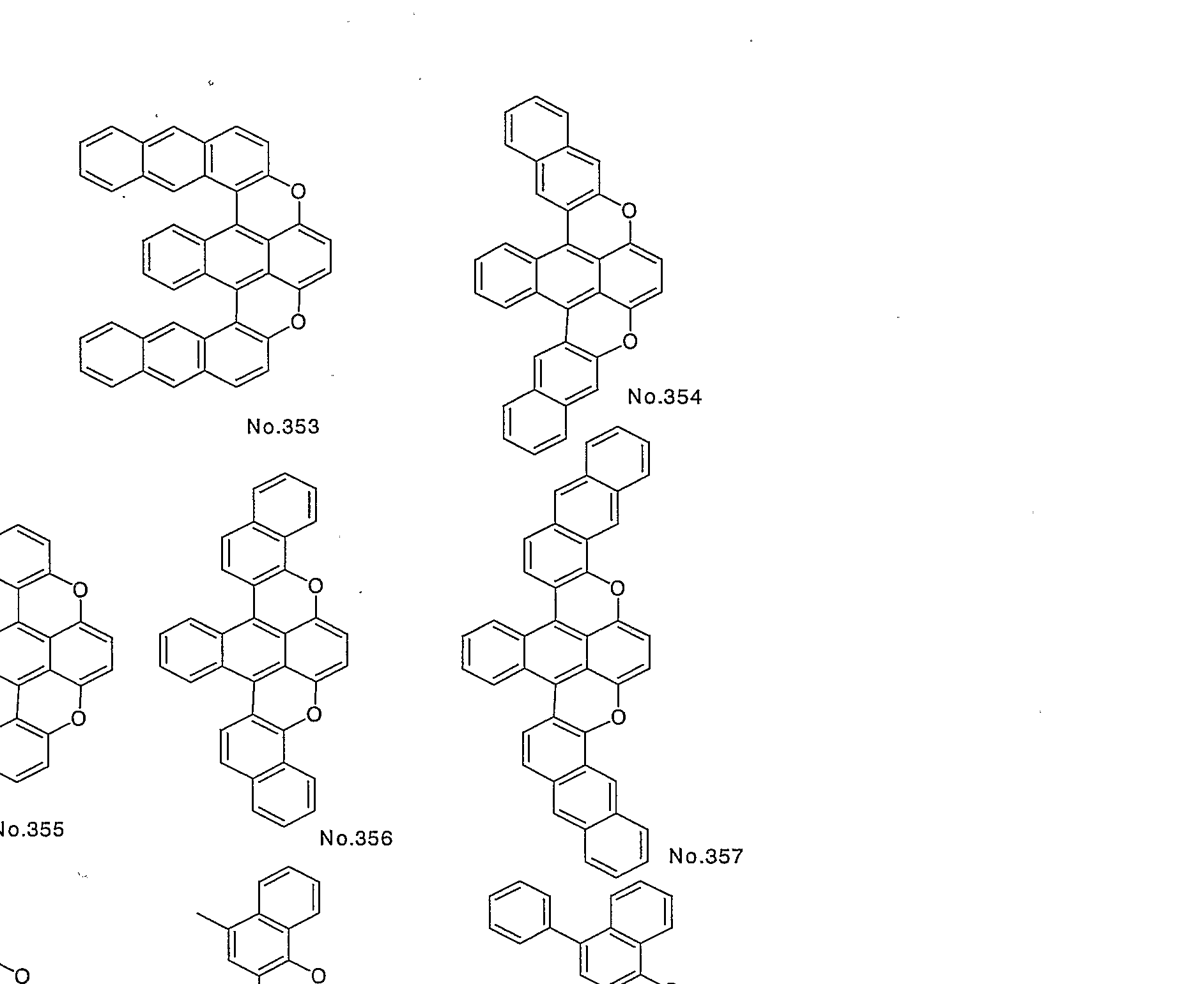

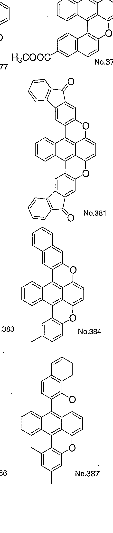


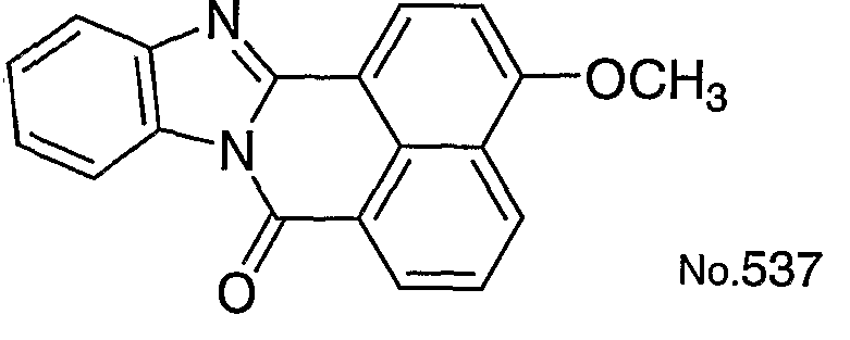
Claims


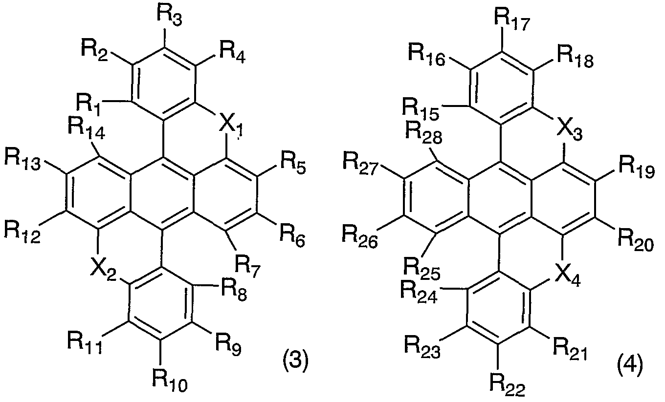


Priority Applications (3)
| Application Number | Priority Date | Filing Date | Title |
|---|---|---|---|
| JP2005508056A JP4606328B2 (ja) | 2003-01-17 | 2004-01-16 | 発光素子、それに用いる縮合多環系化合物及びその製造方法 |
| US10/542,085 US7494721B2 (en) | 2003-01-17 | 2004-01-16 | Light-emitting device, condensed polycyclic compound used therein and method for producing same |
| EP04702858A EP1589089A4 (en) | 2003-01-17 | 2004-01-16 | ELECTROLUMINESCENT DEVICE, CONDENSED POLYCYCLIC COMPOUND USED THEREIN AND PROCESS FOR PRODUCING THE SAME |
Applications Claiming Priority (12)
| Application Number | Priority Date | Filing Date | Title |
|---|---|---|---|
| JP2003-009304 | 2003-01-17 | ||
| JP2003009304 | 2003-01-17 | ||
| JP2003-166799 | 2003-06-11 | ||
| JP2003166799 | 2003-06-11 | ||
| JP2003172896 | 2003-06-18 | ||
| JP2003-172896 | 2003-06-18 | ||
| JP2003-181925 | 2003-06-26 | ||
| JP2003181925 | 2003-06-26 | ||
| JP2003305338A JP2005108441A (ja) | 2003-08-28 | 2003-08-28 | 発光素子 |
| JP2003-305338 | 2003-08-28 | ||
| JP2003-382625 | 2003-11-12 | ||
| JP2003382625A JP2005272301A (ja) | 2003-11-12 | 2003-11-12 | 縮合多環系化合物及びそれを用いた発光素子 |
Publications (1)
| Publication Number | Publication Date |
|---|---|
| WO2004065520A1 true WO2004065520A1 (ja) | 2004-08-05 |
Family
ID=32777350
Family Applications (1)
| Application Number | Title | Priority Date | Filing Date |
|---|---|---|---|
| PCT/JP2004/000306 Ceased WO2004065520A1 (ja) | 2003-01-17 | 2004-01-16 | 発光素子、それに用いる縮合多環系化合物及びその製造方法 |
Country Status (6)
| Country | Link |
|---|---|
| US (1) | US7494721B2 (ja) |
| EP (1) | EP1589089A4 (ja) |
| JP (1) | JP4606328B2 (ja) |
| KR (1) | KR20050095613A (ja) |
| TW (1) | TW200422380A (ja) |
| WO (1) | WO2004065520A1 (ja) |
Cited By (3)
| Publication number | Priority date | Publication date | Assignee | Title |
|---|---|---|---|---|
| KR100690886B1 (ko) * | 2005-06-22 | 2007-03-09 | 한양대학교 산학협력단 | 인광성 유기 발광 소자 및 제조방법 |
| JP2010202599A (ja) * | 2009-03-04 | 2010-09-16 | Idemitsu Kosan Co Ltd | 芳香族化合物、有機電子素子用材料及びそれを用いた有機エレクトロルミネッセンス素子 |
| WO2013021907A1 (ja) * | 2011-08-11 | 2013-02-14 | ユーディーシー アイルランド リミテッド | 有機電界発光素子、該素子用材料、並びに該素子を用いた発光装置、表示装置及び照明装置 |
Families Citing this family (11)
| Publication number | Priority date | Publication date | Assignee | Title |
|---|---|---|---|---|
| DE102005040411A1 (de) * | 2005-08-26 | 2007-03-01 | Merck Patent Gmbh | Neue Materialien für organische Elektrolumineszenzvorrichtungen |
| WO2007094101A1 (ja) * | 2006-02-14 | 2007-08-23 | Sharp Kabushiki Kaisha | 有機エレクトロルミネッセンス装置及び有機エレクトロルミネッセンス表示装置 |
| KR20080088696A (ko) * | 2007-03-30 | 2008-10-06 | 삼성전자주식회사 | 유기 발광 장치 및 이의 제조 방법 |
| US7781076B2 (en) | 2007-06-26 | 2010-08-24 | Eastman Kodak Company | Heteropyrene-based semiconductor materials for electronic devices and methods of making the same |
| US8049411B2 (en) | 2008-06-05 | 2011-11-01 | Idemitsu Kosan Co., Ltd. | Material for organic electroluminescence device and organic electroluminescence device using the same |
| DE102008054141A1 (de) * | 2008-10-31 | 2010-05-06 | Merck Patent Gmbh | Neue Materialien für organische Elektrolumineszenzvorrichtungen |
| US8716700B2 (en) * | 2009-10-29 | 2014-05-06 | E I Du Pont De Nemours And Company | Organic light-emitting diodes having white light emission |
| US8716699B2 (en) * | 2009-10-29 | 2014-05-06 | E I Du Pont De Nemours And Company | Organic light-emitting diodes having white light emission |
| KR20150013633A (ko) * | 2012-05-02 | 2015-02-05 | 바스프 에스이 | 유기 물질의 증착 방법 |
| CN110635053B (zh) * | 2018-06-21 | 2022-06-17 | 上海和辉光电股份有限公司 | p型掺杂材料、包含其的空穴注入材料、空穴注入层和OLED显示面板 |
| US12467308B2 (en) * | 2022-11-23 | 2025-11-11 | LuxWall, Inc. | Vacuum insulated panel with tellurium oxide and/or vanadium oxide inclusive seal |
Citations (2)
| Publication number | Priority date | Publication date | Assignee | Title |
|---|---|---|---|---|
| JPH05222362A (ja) * | 1992-02-14 | 1993-08-31 | Mitsubishi Kasei Corp | 有機電界発光素子 |
| EP0629512A2 (en) * | 1993-06-07 | 1994-12-21 | Minnesota Mining And Manufacturing Company | Reusable heat-sensitive colour imaging material |
Family Cites Families (3)
| Publication number | Priority date | Publication date | Assignee | Title |
|---|---|---|---|---|
| DE2910668C2 (de) * | 1979-03-19 | 1982-07-22 | Hans-Dieter Prof.Dr. Brauer | Lichtempfindliches Aufzeichnungsmaterial und Verwendung von 9,10-Diphenylanthracenderivaten |
| JPH0656777A (ja) * | 1992-08-10 | 1994-03-01 | Nisshinbo Ind Inc | アントラキノニルジカルバゾール類化合物及びベンゾビスインドロアクリジン類化合物 |
| JP4281293B2 (ja) * | 2002-05-10 | 2009-06-17 | セイコーエプソン株式会社 | 電気光学装置の製造方法及び電気光学装置の製造装置 |
-
2004
- 2004-01-16 KR KR1020057013271A patent/KR20050095613A/ko not_active Ceased
- 2004-01-16 TW TW093101140A patent/TW200422380A/zh unknown
- 2004-01-16 EP EP04702858A patent/EP1589089A4/en not_active Withdrawn
- 2004-01-16 WO PCT/JP2004/000306 patent/WO2004065520A1/ja not_active Ceased
- 2004-01-16 US US10/542,085 patent/US7494721B2/en not_active Expired - Fee Related
- 2004-01-16 JP JP2005508056A patent/JP4606328B2/ja not_active Expired - Fee Related
Patent Citations (2)
| Publication number | Priority date | Publication date | Assignee | Title |
|---|---|---|---|---|
| JPH05222362A (ja) * | 1992-02-14 | 1993-08-31 | Mitsubishi Kasei Corp | 有機電界発光素子 |
| EP0629512A2 (en) * | 1993-06-07 | 1994-12-21 | Minnesota Mining And Manufacturing Company | Reusable heat-sensitive colour imaging material |
Non-Patent Citations (7)
| Title |
|---|
| CHRISTENSEN J.B. ET AL.: "Corbienes and dioxapyrenes- new Weitz-type donors", SYNTHETIC METALS, vol. 42, no. 3, 1991, pages 2311 - 2313, XP002904690 * |
| See also references of EP1589089A4 * |
| TOKITA S. ET AL.: "Molecular design and synthesis of novel analogues of benzodixanthene and anthradichromene", MOL. CRYST. LIQ. CRYST., vol. 297, 1997, pages 269 - 276, XP002904689 * |
| TOKITA SUMIO ET AL.: "Benzo [1,2,3-kl:4,5,6-k'l'] dixanthene no hitaishogata ruijitai oyobi sono endoperoxide no gosei to sorera no photochromic tokusei", JOURNAL OF THE CHEMICAL SOCIETY OF JAPAN, no. 10, 1992, pages 1097 - 1101, XP002904685 * |
| TOKITA SUMIO ET AL.: "Benzo [1,2,3-kl:4,5,6-k'l']dixanthene no zokangata ruien kagobutsu narabi ni sorera no endoperoxide no gosei to sorera no photochromic tokusei", JOURNAL OF THE CHEMICAL SOCIETY OF JAPAN, no. 5, 1989, pages 876 - 879, XP002904686 * |
| TOKITA SUMIO ET AL.: "Benzo[1,2,3-kl:4,5,6-k'l']dixanthene no methyl yudotai oyobi sono endoperoxide no gosei to sorera no photochromic tokusei", JOURNAL OF THE CHEMICAL SOCIETY OF JAPAN, no. 5, 1988, pages 814 - 818, XP002904687 * |
| WATANABE T. ET AL.: "Photochromic properties of benzodixanthene analogues having alkyl group and their Langmuir-Blodgett films", J. PHOTOHOLYMER SCI. AND TECHNOL., vol. 11, no. 1, 1998, pages 41 - 46, XP002904688 * |
Cited By (6)
| Publication number | Priority date | Publication date | Assignee | Title |
|---|---|---|---|---|
| KR100690886B1 (ko) * | 2005-06-22 | 2007-03-09 | 한양대학교 산학협력단 | 인광성 유기 발광 소자 및 제조방법 |
| JP2010202599A (ja) * | 2009-03-04 | 2010-09-16 | Idemitsu Kosan Co Ltd | 芳香族化合物、有機電子素子用材料及びそれを用いた有機エレクトロルミネッセンス素子 |
| WO2013021907A1 (ja) * | 2011-08-11 | 2013-02-14 | ユーディーシー アイルランド リミテッド | 有機電界発光素子、該素子用材料、並びに該素子を用いた発光装置、表示装置及び照明装置 |
| JP2013041893A (ja) * | 2011-08-11 | 2013-02-28 | Fujifilm Corp | 有機電界発光素子、該素子用材料、並びに該素子を用いた発光装置、表示装置及び照明装置 |
| US10468607B2 (en) | 2011-08-11 | 2019-11-05 | Udc Ireland Limited | Organic electric light emitting element, material for said element, and light emitting device, display device, and illumination device employing said element |
| US12404264B2 (en) | 2011-08-11 | 2025-09-02 | Udc Ireland Limited | Organic electric light emitting element, material for said element, and light emitting device, display device, and illumination device employing said element |
Also Published As
| Publication number | Publication date |
|---|---|
| EP1589089A4 (en) | 2008-08-27 |
| JPWO2004065520A1 (ja) | 2006-05-18 |
| KR20050095613A (ko) | 2005-09-29 |
| EP1589089A1 (en) | 2005-10-26 |
| JP4606328B2 (ja) | 2011-01-05 |
| US7494721B2 (en) | 2009-02-24 |
| TW200422380A (en) | 2004-11-01 |
| US20060051612A1 (en) | 2006-03-09 |
Similar Documents
| Publication | Publication Date | Title |
|---|---|---|
| JP5938397B2 (ja) | 有機光電子素子用化合物、これを含む有機発光ダイオードおよび前記有機発光ダイオードを含む表示装置 | |
| JP5252482B2 (ja) | 発光素子 | |
| EP2215183B1 (en) | New compound and organic light emitting device using the same | |
| EP2415752B1 (en) | Aromatic amine derivative and organic electroluminescent element using same | |
| KR101317511B1 (ko) | 신규한 화합물 및 이를 이용한 유기 전자 소자 | |
| KR101447961B1 (ko) | 새로운 유기전계발광소자용 화합물 및 그를 포함하는 유기전계발광소자 | |
| JP5590815B2 (ja) | 新規有機化合物および発光素子および画像表示装置 | |
| KR101468493B1 (ko) | 새로운 유기전계발광소자용 화합물 및 그를 포함하는 유기전계발광소자 | |
| KR101499102B1 (ko) | 새로운 유기전계발광소자용 화합물 및 그를 포함하는 유기전계발광소자 | |
| KR20120011445A (ko) | 신규한 유기 발광 화합물 및 이를 포함하는 유기 전계 발광 소자 | |
| KR20120009761A (ko) | 신규한 유기 발광 화합물 및 이를 포함하는 유기 전계 발광 소자 | |
| KR102192691B1 (ko) | 유기발광 화합물 및 이를 포함하는 유기전계발광소자 | |
| JP4052010B2 (ja) | 発光素子用材料およびそれを用いた発光素子 | |
| KR20150070928A (ko) | 유기발광 화합물 및 이를 포함하는 유기전계발광소자 | |
| KR20110134581A (ko) | 신규한 유기 발광 화합물 및 이를 포함하는 유기 전계 발광 소자 | |
| KR101597865B1 (ko) | 신규한 화합물 및 이를 이용한 유기 전자 소자 | |
| KR100893044B1 (ko) | 안트라센 유도체, 이를 이용한 유기 전자 소자 및 이 유기전자 소자를 포함하는 전자 장치 | |
| CN101735107A (zh) | 芳香胺化合物、包含其的有机电致发光元件以及包括有机电致发光元件的显示装置 | |
| KR20120083243A (ko) | 신규한 화합물 및 이를 이용한 유기 전자 소자 | |
| US10224489B2 (en) | Compound and organic electronic device using the same | |
| WO2012086366A1 (en) | Fused polycyclic compound and organic light emitting device using the same | |
| JP4606328B2 (ja) | 発光素子、それに用いる縮合多環系化合物及びその製造方法 | |
| KR20090112137A (ko) | 유기 전기 발광 조성물 및 이를 포함하는 유기 전기 발광소자 | |
| KR101396647B1 (ko) | 신규한 안트라센 유도체, 이의 제조방법 및 이를 이용한 유기전자소자 | |
| JP2014086463A (ja) | 新規縮合多環化合物 |
Legal Events
| Date | Code | Title | Description |
|---|---|---|---|
| AK | Designated states |
Kind code of ref document: A1 Designated state(s): AE AG AL AM AT AU AZ BA BB BG BR BW BY BZ CA CH CN CO CR CU CZ DE DK DM DZ EC EE EG ES FI GB GD GE GH GM HR HU ID IL IN IS JP KE KG KP KR KZ LC LK LR LS LT LU LV MA MD MG MK MN MW MX MZ NA NI NO NZ OM PG PH PL PT RO RU SC SD SE SG SK SL SY TJ TM TN TR TT TZ UA UG US UZ VC VN YU ZA ZM ZW |
|
| AL | Designated countries for regional patents |
Kind code of ref document: A1 Designated state(s): BW GH GM KE LS MW MZ SD SL SZ TZ UG ZM ZW AM AZ BY KG KZ MD RU TJ TM AT BE BG CH CY CZ DE DK EE ES FI FR GB GR HU IE IT LU MC NL PT RO SE SI SK TR BF BJ CF CG CI CM GA GN GQ GW ML MR NE SN TD TG |
|
| 121 | Ep: the epo has been informed by wipo that ep was designated in this application | ||
| ENP | Entry into the national phase |
Ref document number: 2006051612 Country of ref document: US Kind code of ref document: A1 |
|
| WWE | Wipo information: entry into national phase |
Ref document number: 10542085 Country of ref document: US |
|
| WWE | Wipo information: entry into national phase |
Ref document number: 20048021869 Country of ref document: CN Ref document number: 2005508056 Country of ref document: JP |
|
| WWE | Wipo information: entry into national phase |
Ref document number: 1020057013271 Country of ref document: KR |
|
| WWE | Wipo information: entry into national phase |
Ref document number: 2004702858 Country of ref document: EP |
|
| WWP | Wipo information: published in national office |
Ref document number: 1020057013271 Country of ref document: KR |
|
| WWP | Wipo information: published in national office |
Ref document number: 2004702858 Country of ref document: EP |
|
| WWP | Wipo information: published in national office |
Ref document number: 10542085 Country of ref document: US |