WO2004094331A2 - Hermetically sealed glass package and method of fabrication - Google Patents
Hermetically sealed glass package and method of fabricationInfo
- Publication number
- WO2004094331A2 WO2004094331A2 PCT/US2004/007557 US2004007557W WO2004094331A2 WO 2004094331 A2 WO2004094331 A2 WO 2004094331A2 US 2004007557 W US2004007557 W US 2004007557W WO 2004094331 A2 WO2004094331 A2 WO 2004094331A2
- Authority
- WO
- WIPO (PCT)
- Prior art keywords
- doped
- sealing glass
- plate
- glass plate
- glass
- Prior art date
- Legal status (The legal status is an assumption and is not a legal conclusion. Google has not performed a legal analysis and makes no representation as to the accuracy of the status listed.)
- Ceased
Links
Classifications
-
- H—ELECTRICITY
- H05—ELECTRIC TECHNIQUES NOT OTHERWISE PROVIDED FOR
- H05B—ELECTRIC HEATING; ELECTRIC LIGHT SOURCES NOT OTHERWISE PROVIDED FOR; CIRCUIT ARRANGEMENTS FOR ELECTRIC LIGHT SOURCES, IN GENERAL
- H05B33/00—Electroluminescent light sources
- H05B33/02—Details
- H05B33/04—Sealing arrangements, e.g. against humidity
-
- C—CHEMISTRY; METALLURGY
- C03—GLASS; MINERAL OR SLAG WOOL
- C03C—CHEMICAL COMPOSITION OF GLASSES, GLAZES OR VITREOUS ENAMELS; SURFACE TREATMENT OF GLASS; SURFACE TREATMENT OF FIBRES OR FILAMENTS MADE FROM GLASS, MINERALS OR SLAGS; JOINING GLASS TO GLASS OR OTHER MATERIALS
- C03C8/00—Enamels; Glazes; Fusion seal compositions being frit compositions having non-frit additions
- C03C8/24—Fusion seal compositions being frit compositions having non-frit additions, i.e. for use as seals between dissimilar materials, e.g. glass and metal; Glass solders
-
- C—CHEMISTRY; METALLURGY
- C03—GLASS; MINERAL OR SLAG WOOL
- C03C—CHEMICAL COMPOSITION OF GLASSES, GLAZES OR VITREOUS ENAMELS; SURFACE TREATMENT OF GLASS; SURFACE TREATMENT OF FIBRES OR FILAMENTS MADE FROM GLASS, MINERALS OR SLAGS; JOINING GLASS TO GLASS OR OTHER MATERIALS
- C03C27/00—Joining pieces of glass to pieces of other inorganic material; Joining glass to glass other than by fusing
- C03C27/06—Joining glass to glass by processes other than fusing
-
- C—CHEMISTRY; METALLURGY
- C03—GLASS; MINERAL OR SLAG WOOL
- C03C—CHEMICAL COMPOSITION OF GLASSES, GLAZES OR VITREOUS ENAMELS; SURFACE TREATMENT OF GLASS; SURFACE TREATMENT OF FIBRES OR FILAMENTS MADE FROM GLASS, MINERALS OR SLAGS; JOINING GLASS TO GLASS OR OTHER MATERIALS
- C03C3/00—Glass compositions
- C03C3/04—Glass compositions containing silica
- C03C3/076—Glass compositions containing silica with 40% to 90% silica, by weight
- C03C3/089—Glass compositions containing silica with 40% to 90% silica, by weight containing boron
- C03C3/091—Glass compositions containing silica with 40% to 90% silica, by weight containing boron containing aluminium
-
- C—CHEMISTRY; METALLURGY
- C03—GLASS; MINERAL OR SLAG WOOL
- C03C—CHEMICAL COMPOSITION OF GLASSES, GLAZES OR VITREOUS ENAMELS; SURFACE TREATMENT OF GLASS; SURFACE TREATMENT OF FIBRES OR FILAMENTS MADE FROM GLASS, MINERALS OR SLAGS; JOINING GLASS TO GLASS OR OTHER MATERIALS
- C03C3/00—Glass compositions
- C03C3/04—Glass compositions containing silica
- C03C3/076—Glass compositions containing silica with 40% to 90% silica, by weight
- C03C3/089—Glass compositions containing silica with 40% to 90% silica, by weight containing boron
- C03C3/091—Glass compositions containing silica with 40% to 90% silica, by weight containing boron containing aluminium
- C03C3/093—Glass compositions containing silica with 40% to 90% silica, by weight containing boron containing aluminium containing zinc or zirconium
-
- C—CHEMISTRY; METALLURGY
- C03—GLASS; MINERAL OR SLAG WOOL
- C03C—CHEMICAL COMPOSITION OF GLASSES, GLAZES OR VITREOUS ENAMELS; SURFACE TREATMENT OF GLASS; SURFACE TREATMENT OF FIBRES OR FILAMENTS MADE FROM GLASS, MINERALS OR SLAGS; JOINING GLASS TO GLASS OR OTHER MATERIALS
- C03C3/00—Glass compositions
- C03C3/04—Glass compositions containing silica
- C03C3/076—Glass compositions containing silica with 40% to 90% silica, by weight
- C03C3/102—Glass compositions containing silica with 40% to 90% silica, by weight containing lead
- C03C3/108—Glass compositions containing silica with 40% to 90% silica, by weight containing lead containing boron
-
- C—CHEMISTRY; METALLURGY
- C03—GLASS; MINERAL OR SLAG WOOL
- C03C—CHEMICAL COMPOSITION OF GLASSES, GLAZES OR VITREOUS ENAMELS; SURFACE TREATMENT OF GLASS; SURFACE TREATMENT OF FIBRES OR FILAMENTS MADE FROM GLASS, MINERALS OR SLAGS; JOINING GLASS TO GLASS OR OTHER MATERIALS
- C03C8/00—Enamels; Glazes; Fusion seal compositions being frit compositions having non-frit additions
- C03C8/02—Frit compositions, i.e. in a powdered or comminuted form
- C03C8/04—Frit compositions, i.e. in a powdered or comminuted form containing zinc
-
- C—CHEMISTRY; METALLURGY
- C03—GLASS; MINERAL OR SLAG WOOL
- C03C—CHEMICAL COMPOSITION OF GLASSES, GLAZES OR VITREOUS ENAMELS; SURFACE TREATMENT OF GLASS; SURFACE TREATMENT OF FIBRES OR FILAMENTS MADE FROM GLASS, MINERALS OR SLAGS; JOINING GLASS TO GLASS OR OTHER MATERIALS
- C03C8/00—Enamels; Glazes; Fusion seal compositions being frit compositions having non-frit additions
- C03C8/02—Frit compositions, i.e. in a powdered or comminuted form
- C03C8/10—Frit compositions, i.e. in a powdered or comminuted form containing lead
-
- H—ELECTRICITY
- H05—ELECTRIC TECHNIQUES NOT OTHERWISE PROVIDED FOR
- H05B—ELECTRIC HEATING; ELECTRIC LIGHT SOURCES NOT OTHERWISE PROVIDED FOR; CIRCUIT ARRANGEMENTS FOR ELECTRIC LIGHT SOURCES, IN GENERAL
- H05B33/00—Electroluminescent light sources
- H05B33/10—Apparatus or processes specially adapted to the manufacture of electroluminescent light sources
-
- H—ELECTRICITY
- H10—SEMICONDUCTOR DEVICES; ELECTRIC SOLID-STATE DEVICES NOT OTHERWISE PROVIDED FOR
- H10K—ORGANIC ELECTRIC SOLID-STATE DEVICES
- H10K50/00—Organic light-emitting devices
- H10K50/80—Constructional details
- H10K50/84—Passivation; Containers; Encapsulations
- H10K50/841—Self-supporting sealing arrangements
-
- H—ELECTRICITY
- H10—SEMICONDUCTOR DEVICES; ELECTRIC SOLID-STATE DEVICES NOT OTHERWISE PROVIDED FOR
- H10K—ORGANIC ELECTRIC SOLID-STATE DEVICES
- H10K50/00—Organic light-emitting devices
- H10K50/80—Constructional details
- H10K50/84—Passivation; Containers; Encapsulations
- H10K50/842—Containers
- H10K50/8426—Peripheral sealing arrangements, e.g. adhesives, sealants
-
- H—ELECTRICITY
- H10—SEMICONDUCTOR DEVICES; ELECTRIC SOLID-STATE DEVICES NOT OTHERWISE PROVIDED FOR
- H10K—ORGANIC ELECTRIC SOLID-STATE DEVICES
- H10K59/00—Integrated devices, or assemblies of multiple devices, comprising at least one organic light-emitting element covered by group H10K50/00
- H10K59/80—Constructional details
- H10K59/87—Passivation; Containers; Encapsulations
- H10K59/871—Self-supporting sealing arrangements
-
- H—ELECTRICITY
- H10—SEMICONDUCTOR DEVICES; ELECTRIC SOLID-STATE DEVICES NOT OTHERWISE PROVIDED FOR
- H10K—ORGANIC ELECTRIC SOLID-STATE DEVICES
- H10K59/00—Integrated devices, or assemblies of multiple devices, comprising at least one organic light-emitting element covered by group H10K50/00
- H10K59/80—Constructional details
- H10K59/87—Passivation; Containers; Encapsulations
- H10K59/871—Self-supporting sealing arrangements
- H10K59/8722—Peripheral sealing arrangements, e.g. adhesives, sealants
-
- H—ELECTRICITY
- H10—SEMICONDUCTOR DEVICES; ELECTRIC SOLID-STATE DEVICES NOT OTHERWISE PROVIDED FOR
- H10N—ELECTRIC SOLID-STATE DEVICES NOT OTHERWISE PROVIDED FOR
- H10N10/00—Thermoelectric devices comprising a junction of dissimilar materials, i.e. devices exhibiting Seebeck or Peltier effects
- H10N10/80—Constructional details
- H10N10/85—Thermoelectric active materials
- H10N10/856—Thermoelectric active materials comprising organic compositions
Definitions
- the present invention relates to hermetically sealed glass packages that are suitable to protect thin film devices that are sensitive to the ambient environment.
- Some examples of such devices are organic emitting light diode (OLED) displays, sensors, and other optical devices.
- OLED organic emitting light diode
- the present invention is demonstrated using OLED displays as an example. Description of Related Art
- OLEDs have been the subject of a considerable amount of research in recent years because of their use and potential use in a wide variety of electroluminescent devices. For instance, a single OLED can be used in a discrete light emitting device or an array of OLEDs can be used in lighting applications or flat-panel display applications (e.g., OLED displays).
- the OLED displays are known as being very bright and having a good color contrast and wide viewing angle.
- the OLED displays and in particular the electrodes and organic layers located therein are susceptible to degradation resulting from interaction- with oxygen and moisture leaking into the OLED display from the ambient environment.
- the hermetic seal should provide a barrier for oxygen
- the size of the hermetic seal should be minimal (e.g., ⁇ 1 mm) so it does not have an adverse effect on size of the OLED display.
- the temperature generated during the sealing process should not damage the materials (e.g., electrodes and organic layers) within the OLED display.
- the first pixels of OLEDs, which are located about 2 mm from the seal in the OLED display should not be heated to more than 85°C during the sealing process.
- the hermetic seal should enable electrical connections (e.g., thin-film chromium) to enter the OLED display.
- the present invention includes a hermetically sealed OLED display and method for manufacturing the hermetically sealed OLED display.
- the hermetically sealed OLED display is manufactured by providing a first substrate plate and a second substrate plate.
- the second substrate contains at least one transition metal such as iron, copper, vanadium, manganese, cobalt, nickel, chromium and/or neodymium.
- OLEDs are deposited onto the first substrate plate.
- a laser is then used to heat the doped second substrate plate in a manner that causes a portion of it to swell and form a hermetic seal that connects the first substrate plate to the second substrate plate and also protects the OLEDs .
- the second substrate plate is doped with at least one transition metal such that when the laser energy is absorbed there is an increase in temperature in the sealing area.
- FIGURES 1A and IB are a top view and a cross- sectional side view illustrating the basic components of a hermetically sealed OLED display in accordance with a first embodiment of the present invention
- FIGURE 2 is a flowchart illustrating the steps of a preferred method for manufacturing the hermetically sealed OLED display shown in FIGURES 1A and IB;
- FIGURES 3A and 3B are photographs of partial top views of a substrate plate and sealing glass plate that were at least partially sealed to one another using a 20 watt laser and a 25 watt laser in accordance with the method shown in FIGURE 2;
- FIGURE 4 is a graph that shows the profiles of the swelled region on the free surface of the first embodiment of the doped substrate plate that were made using a 810 nm laser operating at 15 watts, 20 watts and 25 watts;
- FIGURE 5 is a graph that shows the height variation of the swelled region shown in FIGURE 4 for the laser operating at 20 watts;
- FIGURE 6 is a graph that shows the thermal expansion curves of a substrate plate (glass code 1737 made by Corning Inc.) and two sealing glass plates
- composition nos. 4-5 that can be used to make glass packages in accordance with the method shown in FIGURE 2;
- FIGURE 7 is a photograph of 1737 substrate plate that was sealed to sealing glass plate (composition no. 5) in experiment #2;
- FIGURE 8 is a photograph of 1737 substrate plate that was sealed to sealing glass plate (composition no. 5) in experiment #3;
- FIGURE 9 is a graph that shows the thermal expansion curves of 1737 and three sealing glass plates
- composition nos. 6-8 that can be used to make glass packages in accordance with the method shown in FIGURE 2;
- FIGURES 10A and 10B are a top view and a cross- sectional side view illustrating the basic components of a hermetically sealed OLED display in accordance with a second embodiment of the present invention
- FIGURE 11 is a flowchart illustrating the steps of a preferred method for manufacturing the hermetically sealed OLED display shown in FIGURES 10A and 10B
- FIGURE 12 is a photograph of a top view of a melted fiber which bonded two substrates together using a 25-watt laser beam in accordance with the method shown in FIGURE 11.
- FIGURES 1-12 there are disclosed in accordance with the present invention two embodiments of hermetically sealed OLED displays 100' and 100'' and methods 200 and 1100 for manufacturing the OLED displays 100' and 100' ' .
- the sealing process of the present invention is described below with respect to the fabrication of hermetically sealed OLED displays 100' and 100'', it should be understood that the same or similar sealing process can be used in other applications to protect sensitive optical/electronic devices that are disposed between two glass plates. Accordingly, the present invention should not be construed in a limited manner .
- FIGURES 1A and IB there are a top view and a cross-sectional side view illustrating the basic components of the first embodiment of the hermetically sealed OLED display 100'.
- the OLED display 100' includes a multilayer sandwich of a substrate plate 102' (e.g., glass plate 102'), an array of OLEDs 104' and a sealing glass plate 106' that was doped with at least one transition metal including iron, copper, vanadium, manganese, cobalt, nickel, chromium or neodymium (for example).
- the OLED display 100' has a hermetic seal 108' formed from the sealing glass plate 106', which protects the OLEDs 104' located between the substrate plate 102' and the sealing glass plate 106'.
- the hermetic seal 108' is typically located just inside the outer edges of the OLED display 100'. And, the OLEDs 104' are located within the perimeter of the hermetic seal 108' . How the hermetic seal 108' is formed from the sealing glass plate 106' and the components such as the laser 110 and lens 114, which are used for forming the hermetic seal 108 ' are described in greater detail below with respect to FIGURES 2-9.
- the substrate plate 102' is provided so that one can make the OLED display 100' .
- the substrate plate 102' is a transparent glass plate like the one manufactured and sold by Corning Incorporated under the brand names of Code 1737 glass or Eagle 2000TM glass.
- the substrate plate 102' can be a transparent glass plate like the ones manufactured and sold by the companies like Asahi Glass Co. (e.g., OA10 glass and OA21 glass), Nippon Electric Glass Co., NHTechno and Samsung Corning Precision Glass Co. (for example).
- the OLEDs 104' and other circuitry are deposited onto the substrate plate 102'.
- the typical OLED 104' includes an anode electrode, one or more organic layers and a cathode electrode.
- any known OLED 104' or future OLED 104' can be used in the OLED display 100'. Again, it should be appreciated that this step can be skipped if an OLED display 100' is not being made but instead a glass package is being made using the sealing process of the present invention.
- the sealing glass plate 106' is provided so that one can make the OLED display 100'.
- the sealing glass plate 106' is made from a borosilicate (multicomponent) glass that is doped with at least one transition metal including iron, copper, vanadium manganese, cobalt, nickel, chromium or neodymium (for example) .
- transition metal including iron, copper, vanadium manganese, cobalt, nickel, chromium or neodymium (for example) .
- a predetermined portion 116' of the sealing glass plate 106' is heated in a manner so that portion 116' of the sealing glass plate 106' can swell and form the hermetic seal 108' (see FIGURE IB).
- the hermetic seal 108' connects and bonds the substrate plate 102' to the sealing glass plate 106'.
- the hermetic seal 108' protects the OLEDs 104' from the ambient environment by preventing oxygen and moisture in the ambient environment from entering into the OLED display 100' .
- the hermetic seal 108' is typically located just inside the outer edges of the OLED display 100'.
- step 208 is performed by using a laser 110 that emits a laser beam 112 through a lens 114 (optional) and through the substrate plate 102' so as to heat the predetermined portion 108' of the doped sealing glass plate 106' (see FIGURE IB).
- the substrate plate 102' does not absorb the laser energy which helps minimize heat dissipation to organic layers in the OLED device.
- the laser beam 112 is moved such that it effectively heats a portion 116' of the doped sealing glass plate 106' and causes that portion 116' of the sealing glass plate 106' to swell and form the hermetic seal 108'.
- the laser 110 has a laser beam 112 with a specific wavelength and the sealing glass plate 106' is doped with metal transition ions so as to enhance it's absorption property at the specific wavelength of the laser beam 112.
- This connection between the laser 110 and sealing glass plate 106' means that when the laser beam 112 is emitted onto the doped sealing glass plate 106' at point 116' there is an increase of absorption of the laser beam 112 at that point 116' which causes the sealing glass plate 106' to swell and form the hermetic seal 108'. Because of the increase in the absorption of heat energy in the doped sealing glass plate 106', the laser beam 112 can move relatively fast over the sealing glass plate 106' and form the hermetic seal 108'.
- the OLEDs 104' should not be heated to more than 85 °C during the operation of the laser 110.
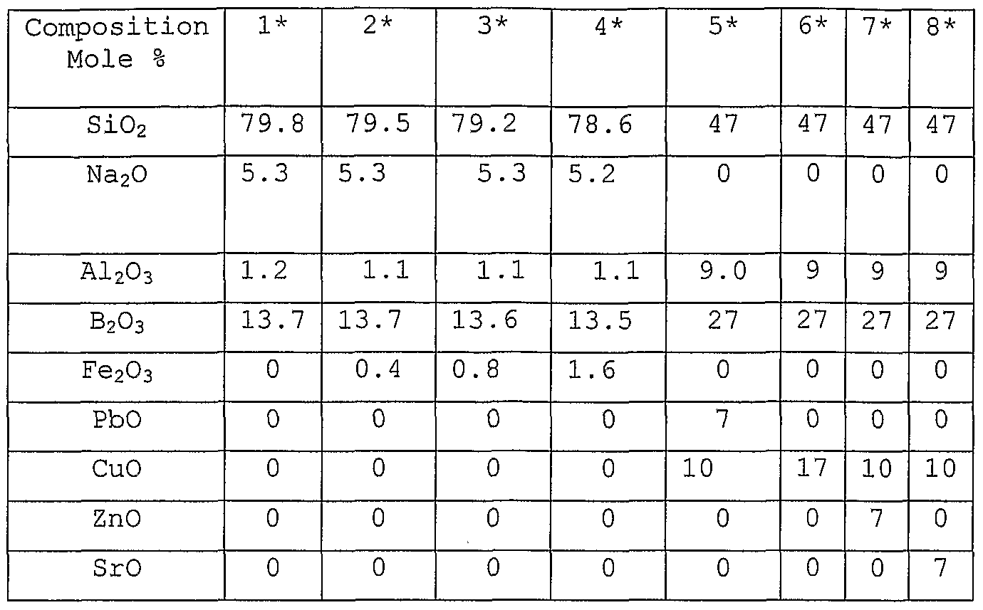
- compositions are associated with the exemplary sealing glass plates 106'.
- each of the exemplary sealing glass plates 106' has a different type and/or concentration of oxides such as Fe 2 0 3 , PbO, CuO, ZnO, and SrO (for example) . It should be noted that some of these elements are not transitional and some of these elements were not added to induce absorption.
- the sealing glass plates 106' in these experiments have an enhanced optical absorption in the near-infrared region and in particular at the 810-nm wavelength.
- the selection of transition- metal dopants is based on the glass absorption at the laser wavelength which in these experiments is 810 nm. The dopants were selected to absorb at the wavelength of the laser beam 112 which in these experiments was 810 nm.
- the substrate plate 102' can be chosen such that it does not absorb at 810 nm. Because the optical absorption of the sealing glass plate 106' is enhanced to correspond with the particular wavelength of the laser 110, the laser 110 is able to move relatively fast to heat the doped sealing glass plate 106' so that it can form the hermetic seal 108' while at the same time not overheat the OLEDs 104' .
- compositions are associated with the exemplary sealing glass plates 106'. v
- the desired degree of laser energy absorption can be achieved by: (1) selecting the particular transition metal (s) to be incorporated within the sealing glass plate 106' and (2) selecting the concentration or amount of transition metal (s) to be incorporated within the sealing glass plate 106'.
- FIGURES 3A and 3B are photographs taken by an optical microscope of partial top views of two plates 102' and 106' that were at least partially connected to one another using a 25 watt laser beam 112.
- seals 108' were obtained when the laser 100 had a power setting of 20 and 25 watts.
- the seals 108' where approximately 250 microns wide in FIGURE 3A and 260 microns wide in FIGURE 3B.
- the sealing glass plate 106' swelled and formed a miniscule or ridge during melting which created a gap of approximately 8 microns between the substrate plate 102' and sealing glass plate 106'. This gap is sufficient to accommodate OLEDs 104' (not present) which are approximately 2 microns thick.
- the profiles of the ridges at various laser powers are shown in the graph of FIGURE 4.
- the height of the ridges ranges from approximately 9 ⁇ m using a 15 watt laser 110 to approximately 12.5 ⁇ m using a 25 watt laser 110.
- the graph in FIGURE 5 shows that the height variation of the ridge made by the 20-watt laser. This ridge is relatively uniform over it's length since its height fluctuates approximately +/- 250nm.
- FIGURE 6 is a graph that shows the thermal expansion curves of the substrate plate 102' (composition no. 9) and two sealing glass plates 106' (composition nos. 4 and 5) .
- the mismatch strain between substrate plate 102' (composition no. 9) and sealing glass plate 106' (composition no. 5) which is 80 ppm is significantly lower when compared to the mismatch strain between substrate plate 102' (composition no.
- sealing glass plate 106' (composition no. 4) which is 360 ppm.
- a laser 110 was used to connect substrate plate 102' (1737 glass substrate ) to sealing glass plate 106' (composition no. 5) cracks were not present when the seal 108' crossed over itself at 90°.
- the sealing glass plate 106' (composition no. 5) is softer and contains more energy absorbing transition metal (s) than sealing glass plate 106' (composition no. 4)
- the laser power required for good sealing was 50% less when compared to the laser power needed to seal the sealing glass plate 106' (composition no. 4) .
- the sealed region was pumped down to a pressure of ⁇ 50 m-torr and helium gas was sprayed around the outer edge of the seal 108'.
- the helium gas leak rate through the seal 108' was measured with a detector.
- the lowest helium leak rate that can be measured with the apparatus was lxlO "8 cc/s.
- the Helium leak rate through the seal 108' was below the detection limit of the instrument. This is indicative of a very good seal 108 ' .
- the sealing glass plate 106' (composition no. 5) contains lead (PbO) in its composition. Glasses containing lead are not generally preferred because of environmental concerns. Therefore, several lead free glass compositions were tested.
- the compositions of these sealing glass plates 106' (composition nos. 6-8) were provided in TABLE 1 and their physical properties are given in Table 2. The thermal expansion curves of sealing glass plates 106'
- composition nos. 6-8) and substrate plate 102' (1737 glass are shown in FIGURE 9. All of these sealing glass plates 106' showed swelling during heating and excellent bonding to substrate plate 102' (1737 glass).
- a sample of sealing glass plate 106' (composition no. 7) was sealed to substrate glass plate 102' (1737 glass) for calcium test. The sealing was done with an 8.5watt laser 110 having a velocity of 15 mm/sec. The sample was aged in 85°C/85RH environment to determine hermetic performance. There was no change in the appearance of the calcium film even though the sample was exposed to this severe moist environment for more than 1800 hours.
- sealing method of the present invention is very rapid and is also amenable to automation.
- sealing a 40x40 cm OLED display 100' can take approximately 2 minutes.
- the doped sealing glass plates 106' can be manufactured using a float glass process, a slot draw process or a rolling process since the glass surface quality is not that critical for the sealing plate of front-emitting OLED displays 100 '..
- FIGURES 10A and 10B there are a top view and a cross-sectional side view illustrating the basic components of a second embodiment of the hermetically sealed OLED display 100''.
- the OLED display 100'' includes a multi-layer sandwich of a first substrate plate 102'' (e.g., glass plate 102''), an array of OLEDs 104'', a sealing glass fiber 106'' that was doped with at least one transition metal including iron, copper, vanadium manganese, cobalt, nickel, chromium or neodymium (for example) and a second substrate plate 107'' (e.g., glass plate 107'').
- a first substrate plate 102'' e.g., glass plate 102''
- an array of OLEDs 104'' e.g., a sealing glass fiber 106'' that was doped with at least one transition metal including iron, copper, vanadium manganese, cobalt, nickel, chromium or
- the OLED display 100'' has a hermetic seal 108 ' ' formed from the sealing glass fiber 106'' which protects the OLEDs 104 ' ' located between the first substrate plate 102'' and the second substrate plate 107''.
- the hermetic seal 108'' is typically located just inside the outer edges of the OLED display 100''. And, the OLEDs 104'' are located within a perimeter of the hermetic seal 108''. How the hermetic seal 108'' is formed from the sealing glass fiber 106'' and the components such as the laser 110 and lens 114 which are used for forming the hermetic seal 108'' are described in greater detail below with respect to the method 1100 and FIGURES 11-12.
- the first substrate plate 102'' is provided so that one can make the OLED display 100''.
- the first substrate plate 102 ' ' is a transparent glass plate like the ones manufactured and sold by Corning Incorporated under the brand names of Code 1737 glass or Eagle 2000TM glass.
- the first substrate plate 102'' can be a transparent glass plate like the ones manufactured and sold by the companies like Asahi Glass Co. (e.g., OA10 glass and OA21 glass), Nippon Electric Glass Co., NHTechno and Samsung Corning Precision Glass Co. (for example).
- the OLEDs 104'' and other circuitry are deposited onto the first substrate plate 102''.
- the typical OLED 104'' includes an anode electrode, one or more organic layers and a cathode electrode.
- any known OLED 104'' or future OLED 104'' can be used in the OLED display 100''. Again, it should be appreciated that this step can be skipped if an OLED display 100' ' is not being made but instead a glass package is being made using the sealing process of the present invention.
- the second substrate plate 107'' is provided so that one can make the OLED display 100''.
- the second substrate plate 107'' is a transparent glass plate like the ones manufactured and sold by Corning Incorporated under , the brand names of Code 1737 glass or Eagle 2000TM glass.
- the second substrate plate 107 ' ' can be a transparent glass plate like the ones manufactured and sold by the companies like Asahi Glass Co. (e.g., OA10 glass and OA21 glass), Nippon Electric Glass Co., NHTechno and Samsung Corning Precision Glass Co. (for example).
- Asahi Glass Co. e.g., OA10 glass and OA21 glass
- Nippon Electric Glass Co. NHTechno and Samsung Corning Precision Glass Co. (for example).
- the sealing glass fiber 106'' is deposited along the edge of the second substrate plate 107''.
- the sealing glass fiber 106'' has a rectangular shape and is made from a silicate glass that is doped with at least one transition metal including iron, copper, vanadium, manganese, coblt, nickel, chromium or neodymium (for example).
- transition metal including iron, copper, vanadium, manganese, coblt, nickel, chromium or neodymium (for example).
- the OLEDs 104'' and other circuitry are placed on the first substrate plate 102 ' ' or on the second substrate plate 107''.
- the typical OLED 104'' includes an anode electrode, one or more organic layers and a cathode electrode.
- any known OLED 104'' or future OLED 104'' can be used in the OLED display 100' ' .
- the sealing glass fiber 106'' is heated by the laser 110 (or other heating mechanism such as an infrared lamp) in a manner so that it can soften and form the hermetic seal 108'' (see FIGURE 10B) .
- the hermetic seal 108'' connects and bonds the first substrate plate 102'' to second substrate plate 107''.
- the hermetic seal 108'' protects the OLEDs 104'* from the ambient environment by preventing oxygen and moisture in the ambient environment from entering into the OLED display 100''.
- the hermetic seal 108'' is typically located just inside the outer edges of the OLED display 100''.
- step 1110 is performed by using a laser 110 that emits a laser beam 112 through a lens 114 (optional) onto the first substrate plate 102'' so as to heat the sealing glass fiber 106''
- the laser beam 112 is moved such that it effectively heats and softens the sealing glass fiber 106'' so that it can form the hermetic seal 108''.
- the hermetic seal 108'' connects the first substrate plate 102 to the second substrate plate 107.
- the laser 110 outputs a laser beam 112 having a specific wavelength (e.g., 800nm wavelength) and the sealing glass fiber 106'' is doped with a transition metal (e.g., vanadium, iron, manganese, cobalt, nickel, chromium and/or neodymium) so as to enhance it's absorption property at the specific wavelength of the laser beam 112.
- a transition metal e.g., vanadium, iron, manganese, cobalt, nickel, chromium and/or neodymium
- This enhancement of the absorption property of the sealing glass fiber 106' ' means that when the laser beam 112 is emitted onto the sealing glass fiber 106' ' there is an increase of absorption of heat energy from the laser beam 112 into the sealing glass fiber 106'' which causes the sealing glass fiber 106'' to soften and form the hermetic seal 108''.
- FIGURE 12 is photograph of a top view of two substrate plates 102'' and 107'' (composition nos.
- the width of the seal 108' ' in Figure 12 is approximately 100 microns.
- the hermetic seal 108' and 108'' has the following properties :
- ⁇ Seal is dense with very low porosity.
- the doped sealing glass plate 106' can be any type of glass that has the ability to swell.
- glasses that have the ability to swell in addition to the ones listed in TABLE 1 include PyrexTM and Corning Codes 7890, 7521 or 7761.
- There are other considerations in addition to having a doped sealing glass 106' and 106'' that can swell which should also be taken into account in order to form a "good" hermetic seal 108' and 108''. These considerations include having the right match between the CTEs and the viscosities of the sealed glasses.
- glass plates 102'' and 107'' can be sealed to one another using the sealing process of the present invention.
- glass plates 102'' and 107'' made by companies such as Asahi Glass Co. (e.g., OA10 glass and OA21 glass), Nippon Electric Glass Co., NHTechno and Samsung Corning Precision Glass Co. can be sealed to one another using the sealing process of the present invention.
- the OLED display 100 can be an active OLED display 100 or a passive OLED display 100.
- the sealing glass plate and sealing glass fiber of the present invention can be designed to absorb heat in other regions besides the infrared region described above.
- a transparent glass plate that exhibits "swelling" behavior can be coated with a thin layer (e.g., 200-400 nm) of material (e.g., silicon, oxides and nitrides of transitional metals) that strongly absorbs laser light at a chosen wavelength.
- a substrate glass plate e.g., Code 1737 glass plate, Eagle 2000TM glass plate
- the coated glass plate are placed together such that the thin layer of material (e.g., silicon, ) is located between the two plates .
- the formation of the hermetic seal can be achieved by irradiating the absorbing interface by moving a laser beam through either the coated glass plate or the substrate glass plate .
- the invention is also ' applicable to other types of optical devices besides OLED displays including field emission displays, plasma displays, inorganic EL displays, and other optical devices where sensitive thin films have to be protected from the environment.
Landscapes
- Chemical & Material Sciences (AREA)
- Engineering & Computer Science (AREA)
- Materials Engineering (AREA)
- Chemical Kinetics & Catalysis (AREA)
- General Chemical & Material Sciences (AREA)
- Geochemistry & Mineralogy (AREA)
- Life Sciences & Earth Sciences (AREA)
- Organic Chemistry (AREA)
- Ceramic Engineering (AREA)
- Physics & Mathematics (AREA)
- Optics & Photonics (AREA)
- Manufacturing & Machinery (AREA)
- Electroluminescent Light Sources (AREA)
Abstract
Description

Claims
Priority Applications (3)
| Application Number | Priority Date | Filing Date | Title |
|---|---|---|---|
| EP04720375A EP1615858A2 (en) | 2003-04-16 | 2004-03-12 | Hermetically sealed glass package and method of fabrication |
| JP2006507114A JP2006524417A (en) | 2003-04-16 | 2004-03-12 | Sealed glass package and manufacturing method thereof |
| CA002522566A CA2522566A1 (en) | 2003-04-16 | 2004-03-12 | Hermetically sealed glass package and method of fabrication |
Applications Claiming Priority (2)
| Application Number | Priority Date | Filing Date | Title |
|---|---|---|---|
| US10/414,653 US20040206953A1 (en) | 2003-04-16 | 2003-04-16 | Hermetically sealed glass package and method of fabrication |
| US10/414,653 | 2003-04-16 |
Publications (2)
| Publication Number | Publication Date |
|---|---|
| WO2004094331A2 true WO2004094331A2 (en) | 2004-11-04 |
| WO2004094331A3 WO2004094331A3 (en) | 2005-08-25 |
Family
ID=33158740
Family Applications (1)
| Application Number | Title | Priority Date | Filing Date |
|---|---|---|---|
| PCT/US2004/007557 Ceased WO2004094331A2 (en) | 2003-04-16 | 2004-03-12 | Hermetically sealed glass package and method of fabrication |
Country Status (7)
| Country | Link |
|---|---|
| US (1) | US20040206953A1 (en) |
| EP (1) | EP1615858A2 (en) |
| JP (1) | JP2006524417A (en) |
| KR (1) | KR20060011831A (en) |
| CN (1) | CN100413801C (en) |
| CA (1) | CA2522566A1 (en) |
| WO (1) | WO2004094331A2 (en) |
Cited By (5)
| Publication number | Priority date | Publication date | Assignee | Title |
|---|---|---|---|---|
| WO2006045067A1 (en) | 2004-10-20 | 2006-04-27 | Corning Incorporated | Optimization of parameters for sealing organic emitting light diode (oled) displays |
| EP1805787A4 (en) * | 2004-10-13 | 2011-02-02 | Corning Inc | HERMETICALLY CLOSED GLASS PACKAGING AND METHOD OF MANUFACTURE |
| US8299705B2 (en) | 2006-01-26 | 2012-10-30 | Samsung Display Co., Ltd. | Organic light emitting display device and manufacturing method thereof |
| US8848749B2 (en) | 2009-05-20 | 2014-09-30 | Samsung Display Co., Ltd. | Light radiating device and method of fabricating organic light emitting diode display device using the same |
| US11800760B2 (en) | 2017-11-15 | 2023-10-24 | Samsung Display Co., Ltd. | Display device having reduced occupied cell seal and realized narrow bezel structure |
Families Citing this family (110)
| Publication number | Priority date | Publication date | Assignee | Title |
|---|---|---|---|---|
| TWI236034B (en) * | 2004-01-09 | 2005-07-11 | Au Optronics Corp | Method for fabricating rear plate of plasma display panel and rear plate fabricated thereby |
| US20050199599A1 (en) * | 2004-03-09 | 2005-09-15 | Xinghua Li | Method of fabrication of hermetically sealed glass package |
| US20060176487A1 (en) | 2004-09-27 | 2006-08-10 | William Cummings | Process control monitors for interferometric modulators |
| US7343080B2 (en) | 2004-09-27 | 2008-03-11 | Idc, Llc | System and method of testing humidity in a sealed MEMS device |
| US7417735B2 (en) | 2004-09-27 | 2008-08-26 | Idc, Llc | Systems and methods for measuring color and contrast in specular reflective devices |
| US7289256B2 (en) | 2004-09-27 | 2007-10-30 | Idc, Llc | Electrical characterization of interferometric modulators |
| US7415186B2 (en) | 2004-09-27 | 2008-08-19 | Idc, Llc | Methods for visually inspecting interferometric modulators for defects |
| US7299681B2 (en) | 2004-09-27 | 2007-11-27 | Idc, Llc | Method and system for detecting leak in electronic devices |
| US7359066B2 (en) | 2004-09-27 | 2008-04-15 | Idc, Llc | Electro-optical measurement of hysteresis in interferometric modulators |
| US7453579B2 (en) | 2004-09-27 | 2008-11-18 | Idc, Llc | Measurement of the dynamic characteristics of interferometric modulators |
| EP1838635A2 (en) * | 2004-12-20 | 2007-10-03 | Corning Incorporated | Method of making a glass envelope |
| KR100640769B1 (en) | 2005-04-15 | 2006-10-31 | 주식회사 대우일렉트로닉스 | OLED Module Manufacturing Method |
| US20070040501A1 (en) * | 2005-08-18 | 2007-02-22 | Aitken Bruce G | Method for inhibiting oxygen and moisture degradation of a device and the resulting device |
| US7722929B2 (en) | 2005-08-18 | 2010-05-25 | Corning Incorporated | Sealing technique for decreasing the time it takes to hermetically seal a device and the resulting hermetically sealed device |
| US7829147B2 (en) | 2005-08-18 | 2010-11-09 | Corning Incorporated | Hermetically sealing a device without a heat treating step and the resulting hermetically sealed device |
| US20080206589A1 (en) * | 2007-02-28 | 2008-08-28 | Bruce Gardiner Aitken | Low tempertature sintering using Sn2+ containing inorganic materials to hermetically seal a device |
| EP2218748B1 (en) * | 2005-09-03 | 2012-10-10 | Samsung SDI Co., Ltd. | Polybenzoxazine-based compound, electrolyte membrane including the same, and fuel cell employing the electrolyte membrane |
| DE102005042229A1 (en) * | 2005-09-05 | 2007-03-08 | Patent-Treuhand-Gesellschaft für elektrische Glühlampen mbH | Glass material and method for heating a glass material |
| US7537504B2 (en) | 2005-12-06 | 2009-05-26 | Corning Incorporated | Method of encapsulating a display element with frit wall and laser beam |
| US7597603B2 (en) | 2005-12-06 | 2009-10-06 | Corning Incorporated | Method of encapsulating a display element |
| EP1958248B1 (en) * | 2005-12-06 | 2016-03-09 | Corning Incorporated | System and method for frit sealing glass packages |
| DE602006021468D1 (en) * | 2005-12-06 | 2011-06-01 | Corning Inc | Manufacturing process for an airtight sealed glass packaging |
| US7636151B2 (en) | 2006-01-06 | 2009-12-22 | Qualcomm Mems Technologies, Inc. | System and method for providing residual stress test structures |
| KR100673765B1 (en) | 2006-01-20 | 2007-01-24 | 삼성에스디아이 주식회사 | Organic light emitting display device and manufacturing method |
| US8038495B2 (en) | 2006-01-20 | 2011-10-18 | Samsung Mobile Display Co., Ltd. | Organic light-emitting display device and manufacturing method of the same |
| KR100635514B1 (en) | 2006-01-23 | 2006-10-18 | 삼성에스디아이 주식회사 | Organic light emitting display device and manufacturing method |
| JP4456092B2 (en) | 2006-01-24 | 2010-04-28 | 三星モバイルディスプレイ株式會社 | Organic electroluminescent display device and manufacturing method thereof |
| JP4624309B2 (en) * | 2006-01-24 | 2011-02-02 | 三星モバイルディスプレイ株式會社 | Organic electroluminescent display device and manufacturing method thereof |
| KR100671641B1 (en) * | 2006-01-25 | 2007-01-19 | 삼성에스디아이 주식회사 | Organic electroluminescent display and manufacturing method thereof |
| KR100685854B1 (en) * | 2006-01-25 | 2007-02-22 | 삼성에스디아이 주식회사 | Organic light emitting display device and manufacturing method |
| KR100688795B1 (en) | 2006-01-25 | 2007-03-02 | 삼성에스디아이 주식회사 | Organic light emitting display device and manufacturing method |
| US8164257B2 (en) | 2006-01-25 | 2012-04-24 | Samsung Mobile Display Co., Ltd. | Organic light emitting display and method of fabricating the same |
| KR100685853B1 (en) * | 2006-01-25 | 2007-02-22 | 삼성에스디아이 주식회사 | Organic light emitting display device and manufacturing method |
| KR100754120B1 (en) * | 2006-02-20 | 2007-08-31 | 삼성에스디아이 주식회사 | Manufacturing method of organic light emitting display device |
| KR100732808B1 (en) * | 2006-01-26 | 2007-06-27 | 삼성에스디아이 주식회사 | Manufacturing method of organic light emitting display device |
| KR100671647B1 (en) | 2006-01-26 | 2007-01-19 | 삼성에스디아이 주식회사 | Organic light emitting display device |
| KR100671639B1 (en) | 2006-01-27 | 2007-01-19 | 삼성에스디아이 주식회사 | Organic electroluminescent display and manufacturing method thereof |
| KR100671643B1 (en) * | 2006-01-27 | 2007-01-19 | 삼성에스디아이 주식회사 | Organic light emitting display device and manufacturing method thereof |
| KR100688789B1 (en) * | 2006-01-27 | 2007-03-02 | 삼성에스디아이 주식회사 | Organic light emitting display device and manufacturing method thereof |
| KR100745344B1 (en) * | 2006-01-27 | 2007-08-02 | 삼성에스디아이 주식회사 | Laser irradiation device |
| US7582952B2 (en) | 2006-02-21 | 2009-09-01 | Qualcomm Mems Technologies, Inc. | Method for providing and removing discharging interconnect for chip-on-glass output leads and structures thereof |
| KR100732817B1 (en) | 2006-03-29 | 2007-06-27 | 삼성에스디아이 주식회사 | Organic light emitting display device and manufacturing method |
| KR100818255B1 (en) | 2006-05-29 | 2008-04-02 | 삼성에스디아이 주식회사 | Polybenzoxazine Compounds, Electrolyte Membranes Containing the Same, and Fuel Cells Employing the Same |
| US7388704B2 (en) | 2006-06-30 | 2008-06-17 | Qualcomm Mems Technologies, Inc. | Determination of interferometric modulator mirror curvature and airgap variation using digital photographs |
| US20080124558A1 (en) * | 2006-08-18 | 2008-05-29 | Heather Debra Boek | Boro-silicate glass frits for hermetic sealing of light emitting device displays |
| KR100745741B1 (en) | 2006-08-22 | 2007-08-02 | 삼성에스디아이 주식회사 | Membrane electrode assembly for fuel cell and fuel cell using same |
| US20080048556A1 (en) * | 2006-08-24 | 2008-02-28 | Stephan Lvovich Logunov | Method for hermetically sealing an OLED display |
| US20080048178A1 (en) * | 2006-08-24 | 2008-02-28 | Bruce Gardiner Aitken | Tin phosphate barrier film, method, and apparatus |
| KR100798151B1 (en) * | 2006-11-09 | 2008-01-28 | 주식회사 엘티에스 | Sealing Method Sealing Method |
| JP2008166197A (en) * | 2006-12-28 | 2008-07-17 | Univ Of Tokyo | Panel body manufacturing method |
| KR100787463B1 (en) * | 2007-01-05 | 2007-12-26 | 삼성에스디아이 주식회사 | Glass frit, composition for forming sealing material, light emitting device and manufacturing method of light emitting device |
| JP2008186697A (en) * | 2007-01-30 | 2008-08-14 | Univ Of Tokyo | Panel body manufacturing method |
| US7652305B2 (en) * | 2007-02-23 | 2010-01-26 | Corning Incorporated | Methods and apparatus to improve frit-sealed glass package |
| KR100850808B1 (en) * | 2007-03-08 | 2008-08-06 | 주식회사 엘티에스 | Sealing material for glass substrate package Sealing method Sealing system |
| US20090014867A1 (en) * | 2007-07-10 | 2009-01-15 | Casey Krawiec | Seal ring for glass wall microelectronics package |
| EP2036912B1 (en) | 2007-09-11 | 2012-08-08 | Samsung Electronics Co., Ltd. | Phosphorous containing benzoxazine-based monomer, polymer thererof, electrode for fuel cell including the same, electrolyte membrane for fuel cell including the same, and fuel cell employing the same |
| EP2036910B1 (en) * | 2007-09-11 | 2012-06-27 | Samsung Electronics Co., Ltd. | Benzoxazine-based monomer, polymer thereof, electrode for fuel cell including the same, electrolyte membrane for fuel cell includind the same, and fuel cell using the same |
| US8247730B2 (en) * | 2007-09-28 | 2012-08-21 | Corning Incorporated | Method and apparatus for frit sealing with a variable laser beam |
| KR101366808B1 (en) * | 2007-10-11 | 2014-02-25 | 삼성전자주식회사 | Polybenzimidazole-base complex, crosslinked material of polybenzoxazines formed thereof, and fuel cell using the same |
| EP2058321B1 (en) | 2007-11-02 | 2014-01-08 | Samsung Electronics Co., Ltd. | Phosphorous containing monomer, polymer thereof, electrode for fuel cell including the polymer, electrolyte membrane for fuel cell including the polymer, and fuel cell using the electrode |
| US8188210B2 (en) * | 2007-11-02 | 2012-05-29 | Samsung Electronics Co., Ltd. | Naphthoxazine benzoxazine-based monomer, polymer thereof, electrode for fuel cell including the polymer, electrolyte membrane for fuel cell including the polymer, and fuel cell using the electrode |
| KR101537311B1 (en) * | 2007-11-02 | 2015-07-17 | 삼성전자주식회사 | Electrolyte membrane for fuel cell and fuel cell using the same |
| EP2062891B1 (en) | 2007-11-06 | 2012-08-08 | Samsung Electronics Co., Ltd. | Benzoxazine-based monomer, polymer thereof, electrode for fuel cell including the polymer, electrolyte membrane for fuel cell including the polymer, and fuel cell using the electrode |
| EP2258009B1 (en) * | 2008-02-28 | 2018-02-14 | Corning Incorporated | Method of sealing a glass envelope |
| KR100927586B1 (en) * | 2008-03-13 | 2009-11-23 | 삼성모바일디스플레이주식회사 | Frit sealing system and manufacturing method of organic light emitting display device using the same |
| KR20090111151A (en) * | 2008-04-21 | 2009-10-26 | 삼성전자주식회사 | OLED display and manufacturing method thereof |
| JP5308718B2 (en) * | 2008-05-26 | 2013-10-09 | 浜松ホトニクス株式会社 | Glass welding method |
| JP5308717B2 (en) | 2008-05-26 | 2013-10-09 | 浜松ホトニクス株式会社 | Glass welding method |
| DE112009001347T5 (en) | 2008-06-11 | 2011-04-21 | Hamamatsu Photonics K.K., Hamamatsu | Melt bonding process for glass |
| CN102066277B (en) | 2008-06-11 | 2013-09-11 | 浜松光子学株式会社 | Glass welding method |
| KR101651300B1 (en) | 2008-06-23 | 2016-08-25 | 하마마츠 포토닉스 가부시키가이샤 | Fusion-bonding process for glass |
| US8440479B2 (en) * | 2009-05-28 | 2013-05-14 | Corning Incorporated | Method for forming an organic light emitting diode device |
| US8568184B2 (en) * | 2009-07-15 | 2013-10-29 | Apple Inc. | Display modules |
| DE102009035392A1 (en) * | 2009-07-30 | 2011-02-03 | Osram Opto Semiconductors Gmbh | Organic component and process for its production |
| KR20120085267A (en) | 2009-09-22 | 2012-07-31 | 코닌클리즈케 필립스 일렉트로닉스 엔.브이. | Glass package for sealing a device, and system comprising glass package |
| JP5481167B2 (en) | 2009-11-12 | 2014-04-23 | 浜松ホトニクス株式会社 | Glass welding method |
| JP5525246B2 (en) | 2009-11-25 | 2014-06-18 | 浜松ホトニクス株式会社 | Glass welding method and glass layer fixing method |
| JP5535588B2 (en) | 2009-11-25 | 2014-07-02 | 浜松ホトニクス株式会社 | Glass welding method and glass layer fixing method |
| JP5466929B2 (en) | 2009-11-25 | 2014-04-09 | 浜松ホトニクス株式会社 | Glass welding method and glass layer fixing method |
| JP5535589B2 (en) | 2009-11-25 | 2014-07-02 | 浜松ホトニクス株式会社 | Glass welding method and glass layer fixing method |
| JP5567319B2 (en) | 2009-11-25 | 2014-08-06 | 浜松ホトニクス株式会社 | Glass welding method and glass layer fixing method |
| JP5481173B2 (en) | 2009-11-25 | 2014-04-23 | 浜松ホトニクス株式会社 | Glass welding method and glass layer fixing method |
| JP5535590B2 (en) | 2009-11-25 | 2014-07-02 | 浜松ホトニクス株式会社 | Glass welding method and glass layer fixing method |
| JP5481172B2 (en) | 2009-11-25 | 2014-04-23 | 浜松ホトニクス株式会社 | Glass welding method and glass layer fixing method |
| KR101193198B1 (en) | 2010-07-12 | 2012-10-26 | 삼성디스플레이 주식회사 | Organic light emitting device and method for preparing the same |
| KR20120077470A (en) | 2010-12-30 | 2012-07-10 | 삼성모바일디스플레이주식회사 | Organic light emitting diode display and fabricating method of the same |
| KR101981811B1 (en) * | 2011-02-18 | 2019-05-23 | 쇼오트 아게 | Feed-through, in particular for batteries and method for integrating said feed-through in a housing by means of ultrasonic welding |
| JP6008546B2 (en) * | 2011-04-13 | 2016-10-19 | 株式会社半導体エネルギー研究所 | Method for manufacturing electroluminescence device |
| TWI433625B (en) | 2011-07-04 | 2014-04-01 | Ind Tech Res Inst | Method for fabricating the flexible electronic device |
| RU2638070C2 (en) * | 2011-09-13 | 2017-12-11 | Ферро Корпорейшн | Induction soldering of inorganic substrates |
| US20140261975A1 (en) * | 2011-11-02 | 2014-09-18 | Ferro Corporation | Microwave Sealing Of Inorganic Substrates Using Low Melting Glass Systems |
| US8841768B2 (en) | 2012-07-23 | 2014-09-23 | Infineon Technologies Ag | Chip package and a method for manufacturing a chip package |
| KR20150052151A (en) * | 2012-08-28 | 2015-05-13 | 엠비-마이크로텍 아게 | Method for producing a hermetic housing for an electronic device |
| US10017849B2 (en) | 2012-11-29 | 2018-07-10 | Corning Incorporated | High rate deposition systems and processes for forming hermetic barrier layers |
| KR101398020B1 (en) * | 2012-11-30 | 2014-05-30 | 주식회사 엘티에스 | Apparatus for sealing frit using laser |
| US9666763B2 (en) | 2012-11-30 | 2017-05-30 | Corning Incorporated | Glass sealing with transparent materials having transient absorption properties |
| CN103910491B (en) * | 2013-01-07 | 2016-10-19 | 中国建筑材料科学研究总院 | There is leaded sealing glass powder and the manufacture method thereof of spectral selection absorption characteristic |
| CN103199199B (en) * | 2013-03-05 | 2016-06-01 | 京东方科技集团股份有限公司 | A kind of OLED packaging film, preparation method and OLED, method for packing |
| CN105377783B (en) | 2013-05-10 | 2019-03-08 | 康宁股份有限公司 | Laser Welding Transparent Glass Sheets Using Low Melting Glass or Thin Absorbent Films |
| EP3008022B1 (en) * | 2013-06-14 | 2020-12-30 | Corning Incorporated | Laminated sealing sheet |
| KR102096053B1 (en) * | 2013-07-25 | 2020-04-02 | 삼성디스플레이 주식회사 | Method for manufacturing organic luminescence emitting display device |
| CN106029592B (en) | 2014-02-13 | 2019-09-03 | 康宁股份有限公司 | Ultra-low melting glass frit and glass fiber |
| US10513455B2 (en) * | 2014-10-30 | 2019-12-24 | Corning Incorporated | Method and apparatus for sealing the edge of a glass article |
| EP3212589A1 (en) | 2014-10-31 | 2017-09-06 | Corning Incorporated | Laser welded glass packages and methods of making |
| CN104966788B (en) * | 2015-07-27 | 2017-02-22 | 京东方科技集团股份有限公司 | Packaging material, organic light-emitting diode device, and packaging method for organic light-emitting diode device |
| JP2018537395A (en) | 2015-11-24 | 2018-12-20 | コーニング インコーポレイテッド | Sealed device housing with particle film initiated thin-wall laser weld and related method |
| WO2018093862A1 (en) | 2016-11-18 | 2018-05-24 | Corning Incorporated | Laser bonded transparent glass-based articles and methods of making the same |
| WO2018093857A1 (en) | 2016-11-18 | 2018-05-24 | Corning Incorporated | Methods of forming laser-induced attributes on glass-based substrates using mid-ir laser |
| KR20220000440A (en) * | 2020-06-25 | 2022-01-04 | 삼성디스플레이 주식회사 | Display device and method of fabricating the same |
| CN114290698B (en) * | 2021-12-24 | 2023-01-31 | 华中科技大学 | High aspect ratio laser processing method of polymer thin film |
Family Cites Families (95)
| Publication number | Priority date | Publication date | Assignee | Title |
|---|---|---|---|---|
| US80463A (en) * | 1868-07-28 | Alexander john b | ||
| US182828A (en) * | 1876-10-03 | Improvement in middlings-separators | ||
| US109136A (en) * | 1870-11-08 | Improvement in gang-plows | ||
| US15620A (en) * | 1856-08-26 | John robertson | ||
| US143258A (en) * | 1873-09-30 | Improvement in devices for cooling millstones | ||
| US3571A (en) * | 1844-04-30 | Epenetus a | ||
| US55841A (en) * | 1866-06-26 | Improved brick-machine | ||
| US8463A (en) * | 1851-10-28 | Mybon cory | ||
| US152800A (en) * | 1874-07-07 | Improvement in dampers | ||
| US49197A (en) * | 1865-08-01 | Improved life-boat | ||
| US187594A (en) * | 1877-02-20 | Improvement in churns | ||
| US33135A (en) * | 1861-08-27 | Improvement in the manufacture of stearic agio | ||
| US45565A (en) * | 1864-12-20 | packer | ||
| US15032A (en) * | 1856-06-03 | Improvement in fire-arms | ||
| US69017A (en) * | 1867-09-17 | Philander perry | ||
| US48234A (en) * | 1865-06-13 | Improved door bell or gong | ||
| US53082A (en) * | 1866-03-06 | Improved apparatus for cooling liquids | ||
| US187254A (en) * | 1877-02-13 | Improvement in irgwiwg-tables | ||
| US190661A (en) * | 1877-05-08 | Improvement in hame-fastenings | ||
| US149312A (en) * | 1874-04-07 | Improvement in rotary tools for dental engines | ||
| US132047A (en) * | 1872-10-08 | Improvement in nut-machines | ||
| US50958A (en) * | 1865-11-14 | Improved malting apparatus | ||
| US154379A (en) * | 1874-08-25 | Improvement in middlings-purifiers | ||
| US31874A (en) * | 1861-04-02 | Improved arrangement of feed-water-heating pipes of steam-engines | ||
| US113763A (en) * | 1871-04-18 | Improvement in cheese-presses | ||
| US125822A (en) * | 1872-04-16 | Improvement in straw-cutters | ||
| US133086A (en) * | 1872-11-19 | Improvement in key-way gages | ||
| US4577A (en) * | 1846-06-16 | Safety-stirrup | ||
| NL6905675A (en) * | 1969-04-12 | 1970-10-14 | ||
| US3723835A (en) * | 1971-07-28 | 1973-03-27 | Motorola Inc | Glasses for encapsulating semiconductor devices |
| US3778126A (en) * | 1971-12-30 | 1973-12-11 | Ibm | Gas display panel without exhaust tube structure |
| JPS526097B2 (en) * | 1972-03-14 | 1977-02-18 | ||
| US3973975A (en) * | 1972-04-21 | 1976-08-10 | Owens-Illinois, Inc. | PbO-containing sealing glass with higher oxide of a cation to avoid PbO reduction |
| JPS5130564B2 (en) * | 1972-10-09 | 1976-09-01 | ||
| US4206382A (en) * | 1978-06-22 | 1980-06-03 | Wagner Electric Corporation | Glass-to-glass sealing method with conductive layer |
| JPS576883A (en) * | 1980-06-13 | 1982-01-13 | Sharp Kk | Thin film el panel |
| US4400870A (en) * | 1980-10-06 | 1983-08-30 | Texas Instruments Incorporated | Method of hermetically encapsulating a semiconductor device by laser irradiation |
| JPH01197169A (en) | 1988-02-01 | 1989-08-08 | Nissan Motor Co Ltd | Motor driven power steering device |
| JPH01225140A (en) * | 1988-03-03 | 1989-09-08 | Nec Corp | Manufacture of semiconductor device |
| JPH01225410A (en) * | 1988-03-04 | 1989-09-08 | Kubota Ltd | Spare seedling supply device for seedling planting device |
| US5500917A (en) * | 1994-04-18 | 1996-03-19 | Gould Electronics Inc. | Optical assembly/housing for securing optical fiber components, devices and fibers to the same or to mounting fixtures |
| JP2754461B2 (en) * | 1994-07-08 | 1998-05-20 | 双葉電子工業株式会社 | Container sealing method and sealing device |
| US5489321A (en) * | 1994-07-14 | 1996-02-06 | Midwest Research Institute | Welding/sealing glass-enclosed space in a vacuum |
| DE69524429T2 (en) * | 1994-09-08 | 2002-05-23 | Idemitsu Kosan Co. Ltd., Tokio/Tokyo | METHOD FOR SEALING AN ORGANIC ELECTROLUMINESCENT ELEMENT AND ORGANIC ELECTROLUMINESCENT ELEMENT |
| US5771562A (en) * | 1995-05-02 | 1998-06-30 | Motorola, Inc. | Passivation of organic devices |
| US5641611A (en) * | 1995-08-21 | 1997-06-24 | Motorola | Method of fabricating organic LED matrices |
| US6195142B1 (en) * | 1995-12-28 | 2001-02-27 | Matsushita Electrical Industrial Company, Ltd. | Organic electroluminescence element, its manufacturing method, and display device using organic electroluminescence element |
| US5734225A (en) * | 1996-07-10 | 1998-03-31 | International Business Machines Corporation | Encapsulation of organic light emitting devices using siloxane or siloxane derivatives |
| JP3957760B2 (en) * | 1996-07-10 | 2007-08-15 | 統寶光電股▲ふん▼有限公司 | Siloxanes and siloxane derivatives as encapsulants for organic light emitting devices |
| US5693956A (en) * | 1996-07-29 | 1997-12-02 | Motorola | Inverted oleds on hard plastic substrate |
| US5895228A (en) * | 1996-11-14 | 1999-04-20 | International Business Machines Corporation | Encapsulation of organic light emitting devices using Siloxane or Siloxane derivatives |
| US5821692A (en) * | 1996-11-26 | 1998-10-13 | Motorola, Inc. | Organic electroluminescent device hermetic encapsulation package |
| US5874804A (en) * | 1997-03-03 | 1999-02-23 | Motorola, Inc. | Organic electroluminescent device hermetic encapsulation package and method of fabrication |
| US5929474A (en) * | 1997-03-10 | 1999-07-27 | Motorola, Inc. | Active matrix OED array |
| US5952778A (en) * | 1997-03-18 | 1999-09-14 | International Business Machines Corporation | Encapsulated organic light emitting device |
| US6356376B1 (en) * | 1997-04-02 | 2002-03-12 | Gentex Corporation | Electrochromic rearview mirror incorporating a third surface metal reflector and a display/signal light |
| US5872355A (en) * | 1997-04-09 | 1999-02-16 | Hewlett-Packard Company | Electroluminescent device and fabrication method for a light detection system |
| US6096496A (en) * | 1997-06-19 | 2000-08-01 | Frankel; Robert D. | Supports incorporating vertical cavity emitting lasers and tracking apparatus for use in combinatorial synthesis |
| US6069443A (en) * | 1997-06-23 | 2000-05-30 | Fed Corporation | Passive matrix OLED display |
| US5920080A (en) * | 1997-06-23 | 1999-07-06 | Fed Corporation | Emissive display using organic light emitting diodes |
| JP3900617B2 (en) * | 1997-09-17 | 2007-04-04 | カシオ計算機株式会社 | LIGHT EMITTING ELEMENT AND PROTECTIVE MATERIAL FOR LIGHT EMITTING ELEMENT |
| US5998805A (en) * | 1997-12-11 | 1999-12-07 | Motorola, Inc. | Active matrix OED array with improved OED cathode |
| US6370019B1 (en) * | 1998-02-17 | 2002-04-09 | Sarnoff Corporation | Sealing of large area display structures |
| US6137221A (en) * | 1998-07-08 | 2000-10-24 | Agilent Technologies, Inc. | Organic electroluminescent device with full color characteristics |
| CN1243105A (en) * | 1998-07-23 | 2000-02-02 | 肖特玻璃制造厂 | Composite welded glass with low melt temp., its filling material and using method thereof |
| US6146225A (en) * | 1998-07-30 | 2000-11-14 | Agilent Technologies, Inc. | Transparent, flexible permeability barrier for organic electroluminescent devices |
| US6268695B1 (en) * | 1998-12-16 | 2001-07-31 | Battelle Memorial Institute | Environmental barrier material for organic light emitting device and method of making |
| DE19918672A1 (en) * | 1999-04-23 | 2000-10-26 | Inst Angewandte Photovoltaik G | Process for welding surfaces of materials |
| US6383664B2 (en) * | 1999-05-11 | 2002-05-07 | The Dow Chemical Company | Electroluminescent or photocell device having protective packaging |
| WO2001012745A1 (en) * | 1999-08-12 | 2001-02-22 | Mitsui Chemicals, Inc. | Photocurable resin composition for sealing material and method of sealing |
| US6552488B1 (en) * | 1999-08-24 | 2003-04-22 | Agilent Technologies, Inc. | Organic electroluminescent device |
| EP1157976A1 (en) * | 1999-10-22 | 2001-11-28 | Nippon Sheet Glass Co., Ltd. | Glass panel and production method therefor |
| WO2002021557A1 (en) * | 2000-09-06 | 2002-03-14 | Osram Opto Semiconductors Gmbh | Encapsulation for oled devices |
| TW526357B (en) * | 1999-12-22 | 2003-04-01 | Matsushita Electric Industrial Co Ltd | Reflective liquid crystal display element and image display device using the same |
| KR100316781B1 (en) * | 2000-02-25 | 2001-12-20 | 김순택 | Method for sealing a glass flat display panel with a frit frame using a laser |
| US6661029B1 (en) * | 2000-03-31 | 2003-12-09 | General Electric Company | Color tunable organic electroluminescent light source |
| US6226890B1 (en) * | 2000-04-07 | 2001-05-08 | Eastman Kodak Company | Desiccation of moisture-sensitive electronic devices |
| US20020003403A1 (en) * | 2000-04-25 | 2002-01-10 | Ghosh Amalkumar P. | Thin film encapsulation of organic light emitting diode devices |
| US6436739B1 (en) * | 2000-04-27 | 2002-08-20 | The Regents Of The University Of California | Thick adherent dielectric films on plastic substrates and method for depositing same |
| US6436222B1 (en) * | 2000-05-12 | 2002-08-20 | Eastman Kodak Company | Forming preformed images in organic electroluminescent devices |
| US6534346B2 (en) * | 2000-05-16 | 2003-03-18 | Nippon Electric Glass Co., Ltd. | Glass and glass tube for encapsulating semiconductors |
| TW463525B (en) * | 2000-06-01 | 2001-11-11 | Ind Tech Res Inst | Organic electroluminescent device and the manufacturing method of the same |
| US6465953B1 (en) * | 2000-06-12 | 2002-10-15 | General Electric Company | Plastic substrates with improved barrier properties for devices sensitive to water and/or oxygen, such as organic electroluminescent devices |
| TW515223B (en) * | 2000-07-24 | 2002-12-21 | Tdk Corp | Light emitting device |
| WO2002042232A1 (en) * | 2000-11-22 | 2002-05-30 | Asahi Glass Company, Limited | Color cathode-ray tube and glass frit for color cathode-ray tube |
| US6611312B2 (en) * | 2001-01-24 | 2003-08-26 | Hitachi, Ltd. | Display device including outer frame with some neighboring wall members that are engaged with each other have oblique surfaces |
| US6614057B2 (en) * | 2001-02-07 | 2003-09-02 | Universal Display Corporation | Sealed organic optoelectronic structures |
| US20030017371A1 (en) * | 2001-06-20 | 2003-01-23 | E.L. Specialists, Inc. | Method for increasing conductivity of conductive translucent layer |
| KR100413450B1 (en) * | 2001-07-20 | 2003-12-31 | 엘지전자 주식회사 | protecting film structure for display device |
| US7701130B2 (en) * | 2001-08-24 | 2010-04-20 | Semiconductor Energy Laboratory Co., Ltd. | Luminous device with conductive film |
| US6470594B1 (en) * | 2001-09-21 | 2002-10-29 | Eastman Kodak Company | Highly moisture-sensitive electronic device element and method for fabrication utilizing vent holes or gaps |
| TW517356B (en) * | 2001-10-09 | 2003-01-11 | Delta Optoelectronics Inc | Package structure of display device and its packaging method |
| US6891330B2 (en) * | 2002-03-29 | 2005-05-10 | General Electric Company | Mechanically flexible organic electroluminescent device with directional light emission |
| DE10219951A1 (en) * | 2002-05-03 | 2003-11-13 | Patent Treuhand Ges Fuer Elektrische Gluehlampen Mbh | Process for encapsulating a component based on organic semiconductors |
| JP2004014267A (en) * | 2002-06-06 | 2004-01-15 | Nippon Sheet Glass Co Ltd | Sealing plate for el element, and mother glass base plate for obtaining multiple sealing plates |
-
2003
- 2003-04-16 US US10/414,653 patent/US20040206953A1/en not_active Abandoned
-
2004
- 2004-03-12 WO PCT/US2004/007557 patent/WO2004094331A2/en not_active Ceased
- 2004-03-12 CN CNB2004800153336A patent/CN100413801C/en not_active Expired - Fee Related
- 2004-03-12 KR KR1020057019458A patent/KR20060011831A/en not_active Ceased
- 2004-03-12 JP JP2006507114A patent/JP2006524417A/en not_active Abandoned
- 2004-03-12 CA CA002522566A patent/CA2522566A1/en not_active Abandoned
- 2004-03-12 EP EP04720375A patent/EP1615858A2/en not_active Withdrawn
Cited By (7)
| Publication number | Priority date | Publication date | Assignee | Title |
|---|---|---|---|---|
| EP1805787A4 (en) * | 2004-10-13 | 2011-02-02 | Corning Inc | HERMETICALLY CLOSED GLASS PACKAGING AND METHOD OF MANUFACTURE |
| WO2006045067A1 (en) | 2004-10-20 | 2006-04-27 | Corning Incorporated | Optimization of parameters for sealing organic emitting light diode (oled) displays |
| US7371143B2 (en) | 2004-10-20 | 2008-05-13 | Corning Incorporated | Optimization of parameters for sealing organic emitting light diode (OLED) displays |
| US8299705B2 (en) | 2006-01-26 | 2012-10-30 | Samsung Display Co., Ltd. | Organic light emitting display device and manufacturing method thereof |
| US8848749B2 (en) | 2009-05-20 | 2014-09-30 | Samsung Display Co., Ltd. | Light radiating device and method of fabricating organic light emitting diode display device using the same |
| US11800760B2 (en) | 2017-11-15 | 2023-10-24 | Samsung Display Co., Ltd. | Display device having reduced occupied cell seal and realized narrow bezel structure |
| US12096668B2 (en) | 2017-11-15 | 2024-09-17 | Samsung Display Co., Ltd. | Display device and method of manufacturing display device |
Also Published As
| Publication number | Publication date |
|---|---|
| WO2004094331A3 (en) | 2005-08-25 |
| EP1615858A2 (en) | 2006-01-18 |
| CN100413801C (en) | 2008-08-27 |
| KR20060011831A (en) | 2006-02-03 |
| CA2522566A1 (en) | 2004-11-04 |
| JP2006524417A (en) | 2006-10-26 |
| CN1798708A (en) | 2006-07-05 |
| US20040206953A1 (en) | 2004-10-21 |
Similar Documents
| Publication | Publication Date | Title |
|---|---|---|
| US20040206953A1 (en) | Hermetically sealed glass package and method of fabrication | |
| US7652305B2 (en) | Methods and apparatus to improve frit-sealed glass package | |
| US8148179B2 (en) | Hermetically sealed glass package and method of fabrication | |
| US6998776B2 (en) | Glass package that is hermetically sealed with a frit and method of fabrication | |
| JP6348943B2 (en) | Glass sealing using transparent material with transient absorption characteristics | |
| EP1897861A1 (en) | Boro-silicate glass frits for hermetic sealing of light emitting device displays | |
| US20040069017A1 (en) | Encapsulation of a display element and method of forming the same | |
| US20130125516A1 (en) | Hermetically sealed glass package and method of manufacture | |
| KR20110094091A (en) | Frit sealing with lasers with high coefficient of thermal expansion and hence sealed glass packages |
Legal Events
| Date | Code | Title | Description |
|---|---|---|---|
| AK | Designated states |
Kind code of ref document: A2 Designated state(s): AE AG AL AM AT AU AZ BA BB BG BR BW BY BZ CA CH CN CO CR CU CZ DE DK DM DZ EC EE EG ES FI GB GD GE GH GM HR HU ID IL IN IS JP KE KG KP KR KZ LC LK LR LS LT LU LV MA MD MG MK MN MW MX MZ NA NI NO NZ OM PG PH PL PT RO RU SC SD SE SG SK SL SY TJ TM TN TR TT TZ UA UG US UZ VC VN YU ZA ZM ZW |
|
| AL | Designated countries for regional patents |
Kind code of ref document: A2 Designated state(s): BW GH GM KE LS MW MZ SD SL SZ TZ UG ZM ZW AM AZ BY KG KZ MD RU TJ TM AT BE BG CH CY CZ DE DK EE ES FI FR GB GR HU IE IT LU MC NL PL PT RO SE SI SK TR BF BJ CF CG CI CM GA GN GQ GW ML MR NE SN TD TG |
|
| 121 | Ep: the epo has been informed by wipo that ep was designated in this application | ||
| WWE | Wipo information: entry into national phase |
Ref document number: 1020057019458 Country of ref document: KR |
|
| WWE | Wipo information: entry into national phase |
Ref document number: 2006507114 Country of ref document: JP Ref document number: 2522566 Country of ref document: CA |
|
| WWE | Wipo information: entry into national phase |
Ref document number: 4784/DELNP/2005 Country of ref document: IN |
|
| WWE | Wipo information: entry into national phase |
Ref document number: 2004720375 Country of ref document: EP |
|
| WWE | Wipo information: entry into national phase |
Ref document number: 20048153336 Country of ref document: CN |
|
| WWP | Wipo information: published in national office |
Ref document number: 2004720375 Country of ref document: EP |
|
| WWP | Wipo information: published in national office |
Ref document number: 1020057019458 Country of ref document: KR |