WO2004107078A1 - 半導体装置 - Google Patents
半導体装置 Download PDFInfo
- Publication number
- WO2004107078A1 WO2004107078A1 PCT/JP2004/005969 JP2004005969W WO2004107078A1 WO 2004107078 A1 WO2004107078 A1 WO 2004107078A1 JP 2004005969 W JP2004005969 W JP 2004005969W WO 2004107078 A1 WO2004107078 A1 WO 2004107078A1
- Authority
- WO
- WIPO (PCT)
- Prior art keywords
- current
- circuit
- current source
- transistor
- load
- Prior art date
- Legal status (The legal status is an assumption and is not a legal conclusion. Google has not performed a legal analysis and makes no representation as to the accuracy of the status listed.)
- Ceased
Links
Classifications
-
- G—PHYSICS
- G09—EDUCATION; CRYPTOGRAPHY; DISPLAY; ADVERTISING; SEALS
- G09G—ARRANGEMENTS OR CIRCUITS FOR CONTROL OF INDICATING DEVICES USING STATIC MEANS TO PRESENT VARIABLE INFORMATION
- G09G3/00—Control arrangements or circuits, of interest only in connection with visual indicators other than cathode-ray tubes
- G09G3/20—Control arrangements or circuits, of interest only in connection with visual indicators other than cathode-ray tubes for presentation of an assembly of a number of characters, e.g. a page, by composing the assembly by combination of individual elements arranged in a matrix no fixed position being assigned to or needed to be assigned to the individual characters or partial characters
- G09G3/22—Control arrangements or circuits, of interest only in connection with visual indicators other than cathode-ray tubes for presentation of an assembly of a number of characters, e.g. a page, by composing the assembly by combination of individual elements arranged in a matrix no fixed position being assigned to or needed to be assigned to the individual characters or partial characters using controlled light sources
- G09G3/30—Control arrangements or circuits, of interest only in connection with visual indicators other than cathode-ray tubes for presentation of an assembly of a number of characters, e.g. a page, by composing the assembly by combination of individual elements arranged in a matrix no fixed position being assigned to or needed to be assigned to the individual characters or partial characters using controlled light sources using electroluminescent panels
- G09G3/32—Control arrangements or circuits, of interest only in connection with visual indicators other than cathode-ray tubes for presentation of an assembly of a number of characters, e.g. a page, by composing the assembly by combination of individual elements arranged in a matrix no fixed position being assigned to or needed to be assigned to the individual characters or partial characters using controlled light sources using electroluminescent panels semiconductive, e.g. using light-emitting diodes [LED]
- G09G3/3208—Control arrangements or circuits, of interest only in connection with visual indicators other than cathode-ray tubes for presentation of an assembly of a number of characters, e.g. a page, by composing the assembly by combination of individual elements arranged in a matrix no fixed position being assigned to or needed to be assigned to the individual characters or partial characters using controlled light sources using electroluminescent panels semiconductive, e.g. using light-emitting diodes [LED] organic, e.g. using organic light-emitting diodes [OLED]
- G09G3/3225—Control arrangements or circuits, of interest only in connection with visual indicators other than cathode-ray tubes for presentation of an assembly of a number of characters, e.g. a page, by composing the assembly by combination of individual elements arranged in a matrix no fixed position being assigned to or needed to be assigned to the individual characters or partial characters using controlled light sources using electroluminescent panels semiconductive, e.g. using light-emitting diodes [LED] organic, e.g. using organic light-emitting diodes [OLED] using an active matrix
- G09G3/3233—Control arrangements or circuits, of interest only in connection with visual indicators other than cathode-ray tubes for presentation of an assembly of a number of characters, e.g. a page, by composing the assembly by combination of individual elements arranged in a matrix no fixed position being assigned to or needed to be assigned to the individual characters or partial characters using controlled light sources using electroluminescent panels semiconductive, e.g. using light-emitting diodes [LED] organic, e.g. using organic light-emitting diodes [OLED] using an active matrix with pixel circuitry controlling the current through the light-emitting element
-
- G—PHYSICS
- G05—CONTROLLING; REGULATING
- G05F—SYSTEMS FOR REGULATING ELECTRIC OR MAGNETIC VARIABLES
- G05F3/00—Non-retroactive systems for regulating electric variables by using an uncontrolled element, or an uncontrolled combination of elements, such element or such combination having self-regulating properties
- G05F3/02—Regulating voltage or current
- G05F3/08—Regulating voltage or current wherein the variable is DC
- G05F3/10—Regulating voltage or current wherein the variable is DC using uncontrolled devices with non-linear characteristics
- G05F3/16—Regulating voltage or current wherein the variable is DC using uncontrolled devices with non-linear characteristics being semiconductor devices
- G05F3/20—Regulating voltage or current wherein the variable is DC using uncontrolled devices with non-linear characteristics being semiconductor devices using diode- transistor combinations
- G05F3/24—Regulating voltage or current wherein the variable is DC using uncontrolled devices with non-linear characteristics being semiconductor devices using diode- transistor combinations wherein the transistors are of the field-effect type only
- G05F3/242—Regulating voltage or current wherein the variable is DC using uncontrolled devices with non-linear characteristics being semiconductor devices using diode- transistor combinations wherein the transistors are of the field-effect type only with compensation for device parameters, e.g. channel width modulation, threshold voltage, processing, or external variations, e.g. temperature, loading, supply voltage
-
- G—PHYSICS
- G09—EDUCATION; CRYPTOGRAPHY; DISPLAY; ADVERTISING; SEALS
- G09G—ARRANGEMENTS OR CIRCUITS FOR CONTROL OF INDICATING DEVICES USING STATIC MEANS TO PRESENT VARIABLE INFORMATION
- G09G2300/00—Aspects of the constitution of display devices
- G09G2300/08—Active matrix structure, i.e. with use of active elements, inclusive of non-linear two terminal elements, in the pixels together with light emitting or modulating elements
- G09G2300/0809—Several active elements per pixel in active matrix panels
- G09G2300/0833—Several active elements per pixel in active matrix panels forming a linear amplifier or follower
-
- G—PHYSICS
- G09—EDUCATION; CRYPTOGRAPHY; DISPLAY; ADVERTISING; SEALS
- G09G—ARRANGEMENTS OR CIRCUITS FOR CONTROL OF INDICATING DEVICES USING STATIC MEANS TO PRESENT VARIABLE INFORMATION
- G09G2300/00—Aspects of the constitution of display devices
- G09G2300/08—Active matrix structure, i.e. with use of active elements, inclusive of non-linear two terminal elements, in the pixels together with light emitting or modulating elements
- G09G2300/0809—Several active elements per pixel in active matrix panels
- G09G2300/0842—Several active elements per pixel in active matrix panels forming a memory circuit, e.g. a dynamic memory with one capacitor
- G09G2300/0861—Several active elements per pixel in active matrix panels forming a memory circuit, e.g. a dynamic memory with one capacitor with additional control of the display period without amending the charge stored in a pixel memory, e.g. by means of additional select electrodes
-
- G—PHYSICS
- G09—EDUCATION; CRYPTOGRAPHY; DISPLAY; ADVERTISING; SEALS
- G09G—ARRANGEMENTS OR CIRCUITS FOR CONTROL OF INDICATING DEVICES USING STATIC MEANS TO PRESENT VARIABLE INFORMATION
- G09G2310/00—Command of the display device
- G09G2310/02—Addressing, scanning or driving the display screen or processing steps related thereto
- G09G2310/0243—Details of the generation of driving signals
- G09G2310/0251—Precharge or discharge of pixel before applying new pixel voltage
-
- G—PHYSICS
- G09—EDUCATION; CRYPTOGRAPHY; DISPLAY; ADVERTISING; SEALS
- G09G—ARRANGEMENTS OR CIRCUITS FOR CONTROL OF INDICATING DEVICES USING STATIC MEANS TO PRESENT VARIABLE INFORMATION
- G09G2320/00—Control of display operating conditions
- G09G2320/02—Improving the quality of display appearance
- G09G2320/029—Improving the quality of display appearance by monitoring one or more pixels in the display panel, e.g. by monitoring a fixed reference pixel
- G09G2320/0295—Improving the quality of display appearance by monitoring one or more pixels in the display panel, e.g. by monitoring a fixed reference pixel by monitoring each display pixel
-
- G—PHYSICS
- G09—EDUCATION; CRYPTOGRAPHY; DISPLAY; ADVERTISING; SEALS
- G09G—ARRANGEMENTS OR CIRCUITS FOR CONTROL OF INDICATING DEVICES USING STATIC MEANS TO PRESENT VARIABLE INFORMATION
- G09G2320/00—Control of display operating conditions
- G09G2320/04—Maintaining the quality of display appearance
- G09G2320/043—Preventing or counteracting the effects of ageing
Definitions
- the present invention provides a
- the brightness varies depending on the current.
- Patent document 1 Patent application public
- Patent Document 2 International Publication No.
- Patent Document 3 Patent application public
- Patent Document 4 International Publication No.
- Patent Documents 1 to 4 disclose V
- Patent Document 4 discloses a circuit configuration for controlling a circuit.
- the above example is for driving in a pixel circuit.
- Patent Document 4 has> Circuit to prevent changes in signal current.
- Patent Document 5 Patent Application Publication Number 2003
- the present invention has been made in view of such a problem
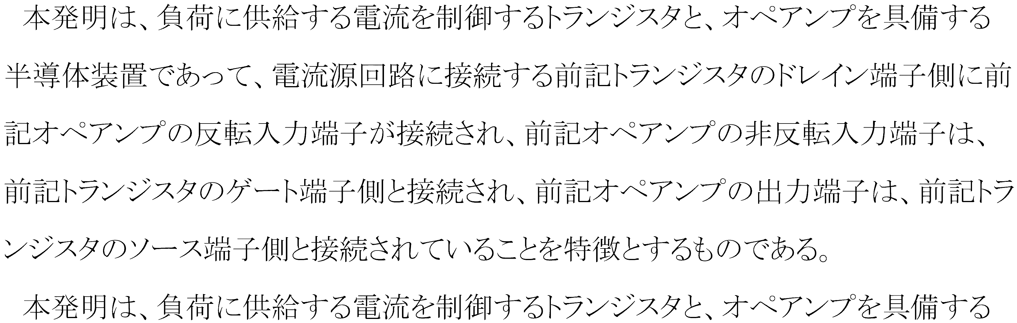
- the present invention provides a method for controlling a current supplied to a load.
- the operation input terminal is connected to the current source circuit.
- the present invention uses the current supplied to the load
- the present invention uses the current supplied to the load
- the feedback is performed using an amplifier circuit.
- FIG. 21 shows a semiconductor device according to the present invention. 22] FIG. 22 shows a semiconductor device of the present invention. 23] FIG. 23 shows a semiconductor device of the present invention.
- FIG. 24 shows a semiconductor device of the present invention.
- FIG. 25 shows a semiconductor device of the present invention.
- FIG. 26 shows a semiconductor device of the present invention.
- FIG. 27 shows a semiconductor device according to the present invention.
- FIG. 28 shows a semiconductor device according to the present invention.
- FIG. 29 shows a semiconductor device of the present invention.
- FIG. 30 shows a semiconductor device of the present invention.
- FIG. 31 shows a semiconductor device of the present invention.
- FIG. 32 shows a semiconductor device of the present invention.
- FIG. 33 shows a semiconductor device according to the present invention.
- FIG. 34 shows a semiconductor device of the present invention.
- the charge transport layer or charge injection layer is not limited to.
- a light emitting element such as an EL element is used.
- Current Idata is the current source transistor 102
- the current source transistor 102 has a current Id
- the current source transistor 102 of the current source is the current source transistor 102 of the current source
- the transistor 102 has a current source circuit 101
- Source transistor 102 flows current Idata
- Width circuit, 208 is the first input terminal, 209
- the first input terminal 108 of circuit 107 is current
- Gate saw of current source transistor 102 Wiring 106 is a current source transistor
- FIGS. As an example of the road,
- a king may arise. In that case,
- Input is connected to output 109.
- transistors 902 and 1002 Reverse to width transistors 901 and 1001
- Embodiment 3 the current from the current source circuit
- the gate potential of the capacitor 102 is
- the current source transistor 102 is saturated
- Figure 18 shows the configuration diagram
- Figure 2 shows the configuration when supplying current.
- the 2302 gate terminal is As a result, switches 1103 and 1104 are on. If you are operating in the
- the amount of current to be supplied is small
- the spontaneity is not particularly limited, the pole with the smaller off-current Fewer! /
- the current source circuit 101 also Affected by 'accurate current Current source circuit 101 in the
- the current source circuit 101 outputs
- the road is connected Y, and if
- the circuit 3104ca is the resource circuit 3101 / or The circuit 3104cb is in a state where the unit can be turned around when the line 3304c is the L signal to the load 11Olca, so that the unit can be united. Also,
- the current source circuit 201 is an image signal
- FIG. Current shown in Fig. 1 (Fig. 11, Fig. 2, Fig. 5)
- Embodiment 6 In this embodiment, a display device will be described.
- the pixel is used for displaying an EL element or the like.
- the present invention can be applied.
- the present invention configures a display unit of an electronic device.
- Image playback device (specifically, Digita
- Figure 43A4 shows a specific example of these electronic devices.
- FIG. 43A shows the light-emitting device ⁇ __ _ luminescence
- FIG. 43E shows a mobile phone equipped with a recording medium.
- Display A13403 mainly displays image information Display, the present invention, the display unit A
- Fig. 43F shows a goggle type data display 13502, arm
- the light emitting device has a light emitting portion.
- Non-light emitting part is back ⁇ : Character information ⁇ ⁇
Landscapes
- Engineering & Computer Science (AREA)
- Physics & Mathematics (AREA)
- Microelectronics & Electronic Packaging (AREA)
- General Physics & Mathematics (AREA)
- Radar, Positioning & Navigation (AREA)
- Theoretical Computer Science (AREA)
- Nonlinear Science (AREA)
- Electromagnetism (AREA)
- Computer Hardware Design (AREA)
- Automation & Control Theory (AREA)
- Control Of Indicators Other Than Cathode Ray Tubes (AREA)
- Electroluminescent Light Sources (AREA)
- Control Of El Displays (AREA)
- Amplifiers (AREA)
- Devices For Indicating Variable Information By Combining Individual Elements (AREA)
- Electronic Switches (AREA)
Abstract
Description


Claims


Priority Applications (3)
| Application Number | Priority Date | Filing Date | Title |
|---|---|---|---|
| JP2004570614A JP4884671B2 (ja) | 2003-05-14 | 2004-05-06 | 半導体装置 |
| EP04731468.7A EP1624358B1 (en) | 2003-05-14 | 2004-05-06 | Semiconductor device |
| KR1020057021361A KR101089050B1 (ko) | 2003-05-14 | 2004-05-06 | 반도체 장치 |
Applications Claiming Priority (2)
| Application Number | Priority Date | Filing Date | Title |
|---|---|---|---|
| JP2003136612 | 2003-05-14 | ||
| JP2003-136612 | 2003-05-14 |
Publications (2)
| Publication Number | Publication Date |
|---|---|
| WO2004107078A1 true WO2004107078A1 (ja) | 2004-12-09 |
| WO2004107078A9 WO2004107078A9 (ja) | 2005-02-03 |
Family
ID=33487087
Family Applications (1)
| Application Number | Title | Priority Date | Filing Date |
|---|---|---|---|
| PCT/JP2004/005969 Ceased WO2004107078A1 (ja) | 2003-05-14 | 2004-05-06 | 半導体装置 |
Country Status (6)
| Country | Link |
|---|---|
| US (3) | US7463223B2 (ja) |
| EP (2) | EP2299429B1 (ja) |
| JP (2) | JP4884671B2 (ja) |
| KR (1) | KR101089050B1 (ja) |
| TW (1) | TWI425864B (ja) |
| WO (1) | WO2004107078A1 (ja) |
Cited By (4)
| Publication number | Priority date | Publication date | Assignee | Title |
|---|---|---|---|---|
| JP2006309172A (ja) * | 2005-03-31 | 2006-11-09 | Semiconductor Energy Lab Co Ltd | 表示装置、表示モジュール、および電子機器 |
| JP2007179040A (ja) * | 2005-12-02 | 2007-07-12 | Semiconductor Energy Lab Co Ltd | 半導体装置 |
| JP2008508547A (ja) * | 2004-07-29 | 2008-03-21 | トムソン ライセンシング | アクティブマトリックス画像ディスプレイ装置及びその制御方法 |
| US8400374B2 (en) | 2005-12-02 | 2013-03-19 | Semiconductor Energy Laboratory Co., Ltd. | Semiconductor device |
Families Citing this family (29)
| Publication number | Priority date | Publication date | Assignee | Title |
|---|---|---|---|---|
| JP2003124757A (ja) * | 2001-10-16 | 2003-04-25 | Texas Instr Japan Ltd | アーリー効果の影響を低減する方法および装置 |
| EP2299429B1 (en) * | 2003-05-14 | 2012-05-16 | Semiconductor Energy Laboratory Co., Ltd. | Semiconductor device |
| CN1802681B (zh) * | 2003-06-06 | 2011-07-13 | 株式会社半导体能源研究所 | 半导体装置 |
| US8378939B2 (en) * | 2003-07-11 | 2013-02-19 | Semiconductor Energy Laboratory Co., Ltd. | Semiconductor device |
| EP1671303B1 (en) * | 2003-09-12 | 2014-08-27 | Semiconductor Energy Laboratory Co., Ltd. | Semiconductor device and driving method of the same |
| CA2443206A1 (en) * | 2003-09-23 | 2005-03-23 | Ignis Innovation Inc. | Amoled display backplanes - pixel driver circuits, array architecture, and external compensation |
| KR101238756B1 (ko) * | 2004-11-24 | 2013-03-06 | 가부시키가이샤 한도오따이 에네루기 켄큐쇼 | 발광 장치, 발광 장치를 포함하는 전자 기기, 및 발광 장치의 구동 방법 |
| FR2878651B1 (fr) * | 2004-12-01 | 2007-06-08 | Commissariat Energie Atomique | Detecteur de neutrons a semi-conducteur |
| US20060120357A1 (en) * | 2004-12-03 | 2006-06-08 | Canon Kabushiki Kaisha | Programming circuit, light emitting device using the same, and display device |
| US20070109284A1 (en) * | 2005-08-12 | 2007-05-17 | Semiconductor Energy Laboratory Co., Ltd. | Display device |
| DE102007038892A1 (de) * | 2007-08-17 | 2009-04-09 | Texas Instruments Deutschland Gmbh | Hochgeschwindigkeits-LED-Treiber |
| JP5736114B2 (ja) | 2009-02-27 | 2015-06-17 | 株式会社半導体エネルギー研究所 | 半導体装置の駆動方法、電子機器の駆動方法 |
| DE102009055891A1 (de) * | 2009-11-26 | 2011-06-09 | Siemens Aktiengesellschaft | Breitbandiger, hochlinearer LED-Verstärker mit hoher Ausgangsleistung in kompakter Bauform |
| US9793039B1 (en) | 2011-05-04 | 2017-10-17 | The Board Of Trustees Of The University Of Alabama | Carbon nanotube-based integrated power inductor for on-chip switching power converters |
| US8922464B2 (en) | 2011-05-11 | 2014-12-30 | Semiconductor Energy Laboratory Co., Ltd. | Active matrix display device and driving method thereof |
| JP5032684B1 (ja) * | 2011-05-27 | 2012-09-26 | 株式会社東芝 | 発光装置、表示装置、及び有機電界発光素子の駆動方法 |
| US8710505B2 (en) | 2011-08-05 | 2014-04-29 | Semiconductor Energy Laboratory Co., Ltd. | Semiconductor device |
| KR20230098374A (ko) | 2011-10-18 | 2023-07-03 | 가부시키가이샤 한도오따이 에네루기 켄큐쇼 | 발광 장치 |
| US12176356B2 (en) | 2011-10-18 | 2024-12-24 | Semiconductor Energy Laboratory Co., Ltd. | Semiconductor device including transistor and light-emitting element |
| US10043794B2 (en) | 2012-03-22 | 2018-08-07 | Semiconductor Energy Laboratory Co., Ltd. | Semiconductor device and electronic device |
| US9590514B1 (en) * | 2013-03-15 | 2017-03-07 | The Board Of Trustees Of The University Of Alabama, For And On Behalf Of The University Of Alabama | Carbon nanotube-based integrated power converters |
| US9172363B2 (en) * | 2013-10-25 | 2015-10-27 | Infineon Technologies Austria Ag | Driving an MOS transistor with constant precharging |
| DE102014207478A1 (de) * | 2014-04-17 | 2015-10-22 | Robert Bosch Gmbh | Verfahren und Vorrichtung zur Ermittlung eines Isolationswiderstandes sowie Hochvoltbatteriesystem mit einer solchen Vorrichtung |
| KR102405182B1 (ko) * | 2015-08-06 | 2022-06-08 | 삼성디스플레이 주식회사 | 부스팅 전압 발생 회로 및 이를 포함하는 표시 장치 |
| US10545612B2 (en) * | 2015-12-11 | 2020-01-28 | Semiconductor Energy Laboratory Co., Ltd. | Signal processing circuit, signal processing IC, and semiconductor device |
| US9984624B2 (en) * | 2015-12-28 | 2018-05-29 | Semiconductor Energy Laboratory Co., Ltd. | Semiconductor device, driver IC, and electronic device |
| WO2018163021A1 (en) | 2017-03-07 | 2018-09-13 | Semiconductor Energy Laboratory Co., Ltd. | Ic, driver ic, display system, and electronic device |
| CN108806595A (zh) * | 2018-06-26 | 2018-11-13 | 京东方科技集团股份有限公司 | 像素驱动电路及方法、显示面板 |
| JP6656330B1 (ja) * | 2018-09-21 | 2020-03-04 | 浜松ホトニクス株式会社 | 固体撮像装置 |
Citations (2)
| Publication number | Priority date | Publication date | Assignee | Title |
|---|---|---|---|---|
| JPH11149783A (ja) * | 1997-11-14 | 1999-06-02 | Hitachi Ltd | 半導体集積回路及びデータ処理システム |
| JP2000112548A (ja) * | 1998-10-07 | 2000-04-21 | Ricoh Co Ltd | 基準電圧発生回路 |
Family Cites Families (49)
| Publication number | Priority date | Publication date | Assignee | Title |
|---|---|---|---|---|
| JPS6261410A (ja) * | 1985-09-11 | 1987-03-18 | Toshiba Corp | カレントミラ−回路 |
| US4742292A (en) | 1987-03-06 | 1988-05-03 | International Business Machines Corp. | CMOS Precision voltage reference generator |
| US5604417A (en) | 1991-12-19 | 1997-02-18 | Hitachi, Ltd. | Semiconductor integrated circuit device |
| FR2714547B1 (fr) * | 1993-12-23 | 1996-01-12 | Commissariat Energie Atomique | Système de commande d'actionneurs à courant continu en électronique de puissance. |
| EP0661715B1 (en) | 1993-12-31 | 1999-06-09 | STMicroelectronics S.r.l. | Non-volatile electrically programmable semiconductor memory device comprising a voltage regulator |
| US5646518A (en) * | 1994-11-18 | 1997-07-08 | Lucent Technologies Inc. | PTAT current source |
| US5585749A (en) | 1994-12-27 | 1996-12-17 | Motorola, Inc. | High current driver providing battery overload protection |
| KR960027254A (ko) * | 1994-12-29 | 1996-07-22 | 조백제 | 선형성이 양호한 오퍼레이션널 트랜스콘덕턴스 증폭기 |
| US6229506B1 (en) | 1997-04-23 | 2001-05-08 | Sarnoff Corporation | Active matrix light emitting diode pixel structure and concomitant method |
| JP4251377B2 (ja) | 1997-04-23 | 2009-04-08 | 宇東科技股▲ふん▼有限公司 | アクティブマトリックス発光ダイオードピクセル構造及び方法 |
| JP3031312B2 (ja) * | 1997-09-11 | 2000-04-10 | 日本電気株式会社 | ドライバ回路及び液晶駆動用半導体装置、並びにそれらの駆動方法 |
| GB9812742D0 (en) | 1998-06-12 | 1998-08-12 | Philips Electronics Nv | Active matrix electroluminescent display devices |
| JP3315652B2 (ja) | 1998-09-07 | 2002-08-19 | キヤノン株式会社 | 電流出力回路 |
| JP3506219B2 (ja) * | 1998-12-16 | 2004-03-15 | シャープ株式会社 | Da変換器およびそれを用いた液晶駆動装置 |
| JP4627822B2 (ja) | 1999-06-23 | 2011-02-09 | 株式会社半導体エネルギー研究所 | 表示装置 |
| JP4126909B2 (ja) | 1999-07-14 | 2008-07-30 | ソニー株式会社 | 電流駆動回路及びそれを用いた表示装置、画素回路、並びに駆動方法 |
| JP4240691B2 (ja) * | 1999-11-01 | 2009-03-18 | 株式会社デンソー | 定電流回路 |
| TW525122B (en) | 1999-11-29 | 2003-03-21 | Semiconductor Energy Lab | Electronic device |
| JP4194237B2 (ja) | 1999-12-28 | 2008-12-10 | 株式会社リコー | 電界効果トランジスタを用いた電圧発生回路及び基準電圧源回路 |
| JP3412599B2 (ja) * | 2000-04-19 | 2003-06-03 | 株式会社デンソー | 半導体装置 |
| US6285177B1 (en) * | 2000-05-08 | 2001-09-04 | Impala Linear Corporation | Short-circuit current-limit circuit |
| JP2001326542A (ja) * | 2000-05-16 | 2001-11-22 | Texas Instr Japan Ltd | 増幅器 |
| JP4579377B2 (ja) * | 2000-06-28 | 2010-11-10 | ルネサスエレクトロニクス株式会社 | 多階調デジタル映像データを表示するための駆動回路及びその方法 |
| JP3700558B2 (ja) * | 2000-08-10 | 2005-09-28 | 日本電気株式会社 | 駆動回路 |
| JP3751812B2 (ja) * | 2000-09-21 | 2006-03-01 | 株式会社東芝 | カスコードトランジスタを出力段に有する電子回路装置 |
| JP4663094B2 (ja) | 2000-10-13 | 2011-03-30 | 株式会社半導体エネルギー研究所 | 半導体装置 |
| US7015882B2 (en) | 2000-11-07 | 2006-03-21 | Sony Corporation | Active matrix display and active matrix organic electroluminescence display |
| JP2003195815A (ja) | 2000-11-07 | 2003-07-09 | Sony Corp | アクティブマトリクス型表示装置およびアクティブマトリクス型有機エレクトロルミネッセンス表示装置 |
| US6661180B2 (en) | 2001-03-22 | 2003-12-09 | Semiconductor Energy Laboratory Co., Ltd. | Light emitting device, driving method for the same and electronic apparatus |
| JP4155389B2 (ja) | 2001-03-22 | 2008-09-24 | 株式会社半導体エネルギー研究所 | 発光装置、その駆動方法及び電子機器 |
| JP2003043994A (ja) | 2001-07-27 | 2003-02-14 | Canon Inc | アクティブマトリックス型ディスプレイ |
| JP2003043993A (ja) | 2001-07-27 | 2003-02-14 | Canon Inc | アクティブマトリックス型ディスプレイ |
| JP3800050B2 (ja) | 2001-08-09 | 2006-07-19 | 日本電気株式会社 | 表示装置の駆動回路 |
| US6489835B1 (en) * | 2001-08-28 | 2002-12-03 | Lattice Semiconductor Corporation | Low voltage bandgap reference circuit |
| JP2003108069A (ja) | 2001-09-27 | 2003-04-11 | Canon Inc | 発光素子の駆動回路 |
| JP3859483B2 (ja) * | 2001-10-26 | 2006-12-20 | 沖電気工業株式会社 | 駆動回路 |
| US7742064B2 (en) | 2001-10-30 | 2010-06-22 | Semiconductor Energy Laboratory Co., Ltd | Signal line driver circuit, light emitting device and driving method thereof |
| US7576734B2 (en) | 2001-10-30 | 2009-08-18 | Semiconductor Energy Laboratory Co., Ltd. | Signal line driving circuit, light emitting device, and method for driving the same |
| US7180479B2 (en) | 2001-10-30 | 2007-02-20 | Semiconductor Energy Laboratory Co., Ltd. | Signal line drive circuit and light emitting device and driving method therefor |
| US6963336B2 (en) | 2001-10-31 | 2005-11-08 | Semiconductor Energy Laboratory Co., Ltd. | Signal line driving circuit and light emitting device |
| US7193619B2 (en) | 2001-10-31 | 2007-03-20 | Semiconductor Energy Laboratory Co., Ltd. | Signal line driving circuit and light emitting device |
| DE10303427A1 (de) * | 2002-02-06 | 2003-10-16 | Nec Corp Tokio Tokyo | Verstärker-Schaltung, Treiber-Schaltung für ein Anzeigegerät , tragbares Telefon und tragbares elektronisches Gerät |
| JP2003322274A (ja) * | 2002-04-26 | 2003-11-14 | Tgk Co Ltd | 電磁制御弁 |
| JP2004107078A (ja) | 2002-09-20 | 2004-04-08 | Anritsu Sanki System Co Ltd | 自動供給トラフ |
| US20050259054A1 (en) | 2003-04-14 | 2005-11-24 | Jie-Farn Wu | Method of driving organic light emitting diode |
| JP4558509B2 (ja) | 2003-04-25 | 2010-10-06 | 株式会社半導体エネルギー研究所 | 半導体装置、表示装置、及び電子機器 |
| EP2299429B1 (en) | 2003-05-14 | 2012-05-16 | Semiconductor Energy Laboratory Co., Ltd. | Semiconductor device |
| CN1802681B (zh) | 2003-06-06 | 2011-07-13 | 株式会社半导体能源研究所 | 半导体装置 |
| US6873200B2 (en) | 2003-08-01 | 2005-03-29 | Rohde & Schwarz Gmbh & Co. Kg | Electronic switch |
-
2004
- 2004-05-06 EP EP10015781A patent/EP2299429B1/en not_active Expired - Lifetime
- 2004-05-06 WO PCT/JP2004/005969 patent/WO2004107078A1/ja not_active Ceased
- 2004-05-06 JP JP2004570614A patent/JP4884671B2/ja not_active Expired - Fee Related
- 2004-05-06 EP EP04731468.7A patent/EP1624358B1/en not_active Expired - Lifetime
- 2004-05-06 KR KR1020057021361A patent/KR101089050B1/ko not_active Expired - Fee Related
- 2004-05-12 US US10/843,680 patent/US7463223B2/en not_active Expired - Fee Related
- 2004-05-13 TW TW093113507A patent/TWI425864B/zh not_active IP Right Cessation
-
2008
- 2008-12-04 US US12/327,883 patent/US8289238B2/en not_active Expired - Fee Related
-
2011
- 2011-05-05 JP JP2011103346A patent/JP5448266B2/ja not_active Expired - Fee Related
-
2012
- 2012-07-25 US US13/557,299 patent/US9576526B2/en not_active Expired - Fee Related
Patent Citations (2)
| Publication number | Priority date | Publication date | Assignee | Title |
|---|---|---|---|---|
| JPH11149783A (ja) * | 1997-11-14 | 1999-06-02 | Hitachi Ltd | 半導体集積回路及びデータ処理システム |
| JP2000112548A (ja) * | 1998-10-07 | 2000-04-21 | Ricoh Co Ltd | 基準電圧発生回路 |
Non-Patent Citations (1)
| Title |
|---|
| See also references of EP1624358A4 * |
Cited By (5)
| Publication number | Priority date | Publication date | Assignee | Title |
|---|---|---|---|---|
| JP2008508547A (ja) * | 2004-07-29 | 2008-03-21 | トムソン ライセンシング | アクティブマトリックス画像ディスプレイ装置及びその制御方法 |
| JP2006309172A (ja) * | 2005-03-31 | 2006-11-09 | Semiconductor Energy Lab Co Ltd | 表示装置、表示モジュール、および電子機器 |
| JP2007179040A (ja) * | 2005-12-02 | 2007-07-12 | Semiconductor Energy Lab Co Ltd | 半導体装置 |
| US8400374B2 (en) | 2005-12-02 | 2013-03-19 | Semiconductor Energy Laboratory Co., Ltd. | Semiconductor device |
| KR101325789B1 (ko) * | 2005-12-02 | 2013-11-04 | 가부시키가이샤 한도오따이 에네루기 켄큐쇼 | 반도체 디바이스 |
Also Published As
| Publication number | Publication date |
|---|---|
| KR20060010791A (ko) | 2006-02-02 |
| TW200511885A (en) | 2005-03-16 |
| WO2004107078A9 (ja) | 2005-02-03 |
| US20050057189A1 (en) | 2005-03-17 |
| US9576526B2 (en) | 2017-02-21 |
| EP1624358A1 (en) | 2006-02-08 |
| US20120286697A1 (en) | 2012-11-15 |
| KR101089050B1 (ko) | 2011-12-02 |
| EP1624358A4 (en) | 2008-01-23 |
| JP5448266B2 (ja) | 2014-03-19 |
| US8289238B2 (en) | 2012-10-16 |
| JPWO2004107078A1 (ja) | 2006-07-20 |
| JP4884671B2 (ja) | 2012-02-29 |
| EP2299429A1 (en) | 2011-03-23 |
| US20090134920A1 (en) | 2009-05-28 |
| EP2299429B1 (en) | 2012-05-16 |
| EP1624358B1 (en) | 2015-03-11 |
| TWI425864B (zh) | 2014-02-01 |
| US7463223B2 (en) | 2008-12-09 |
| JP2011191776A (ja) | 2011-09-29 |
Similar Documents
| Publication | Publication Date | Title |
|---|---|---|
| WO2004107078A1 (ja) | 半導体装置 | |
| JP5178863B2 (ja) | 半導体装置および電子機器 | |
| US7940239B2 (en) | Semiconductor device and display device utilizing the same | |
| JP5493034B2 (ja) | 半導体装置 | |
| TWI244630B (en) | Display device | |
| JP4558509B2 (ja) | 半導体装置、表示装置、及び電子機器 | |
| CN1858839B (zh) | 显示装置的驱动方法 | |
| US20070229417A1 (en) | Flexible Display Device | |
| JP2004088158A (ja) | 電子回路、電気光学装置及び電子機器 | |
| US8085226B2 (en) | Semiconductor device | |
| JP5127556B2 (ja) | 半導体装置及び電子機器 | |
| JP2004201297A (ja) | アナログ回路及びそれを用いた表示装置並びに電子機器 | |
| JP5291865B2 (ja) | 表示装置、表示モジュールおよび電子機器 |
Legal Events
| Date | Code | Title | Description |
|---|---|---|---|
| WWE | Wipo information: entry into national phase |
Ref document number: 2004570614 Country of ref document: JP |
|
| AK | Designated states |
Kind code of ref document: A1 Designated state(s): AE AG AL AM AT AU AZ BA BB BG BR BW BY BZ CA CH CN CO CR CU CZ DE DK DM DZ EC EE EG ES FI GB GD GE GH GM HR HU ID IL IN IS JP KE KG KP KR KZ LC LK LR LS LT LU LV MA MD MG MK MN MW MX MZ NA NI NO NZ OM PG PH PL PT RO RU SC SD SE SG SK SL SY TJ TM TN TR TT TZ UA UG US UZ VC VN YU ZA ZM ZW |
|
| AL | Designated countries for regional patents |
Kind code of ref document: A1 Designated state(s): BW GH GM KE LS MW MZ NA SD SL SZ TZ UG ZM ZW AM AZ BY KG KZ MD RU TJ TM AT BE BG CH CY CZ DE DK EE ES FI FR GB GR HU IE IT LU MC NL PL PT RO SE SI SK TR BF BJ CF CG CI CM GA GN GQ GW ML MR NE SN TD TG |
|
| 121 | Ep: the epo has been informed by wipo that ep was designated in this application | ||
| COP | Corrected version of pamphlet |
Free format text: PAGES 1-28, DESCRIPTION, REPLACED BY CORRECT PAGES 1-28; PAGES 29-35, CLAIMS, REPLACED BY CORRECT PAGES 29-35; PAGES 1/17-17/17, DRAWINGS, REPLACED BY CORRECT PAGES 1/17-17/17; DUE TO AN ERROR DURING THE TECHNICAL PREPARATION FOR INTERNATIONAL PUBLICATION. |
|
| WWE | Wipo information: entry into national phase |
Ref document number: 2004731468 Country of ref document: EP |
|
| WWE | Wipo information: entry into national phase |
Ref document number: 1020057021361 Country of ref document: KR |
|
| WWP | Wipo information: published in national office |
Ref document number: 1020057021361 Country of ref document: KR |
|
| WWP | Wipo information: published in national office |
Ref document number: 2004731468 Country of ref document: EP |