WO2004108283A1 - 光触媒部材 - Google Patents
光触媒部材 Download PDFInfo
- Publication number
- WO2004108283A1 WO2004108283A1 PCT/JP2004/008022 JP2004008022W WO2004108283A1 WO 2004108283 A1 WO2004108283 A1 WO 2004108283A1 JP 2004008022 W JP2004008022 W JP 2004008022W WO 2004108283 A1 WO2004108283 A1 WO 2004108283A1
- Authority
- WO
- WIPO (PCT)
- Prior art keywords
- layer
- photocatalyst
- member according
- heat
- photocatalyst member
- Prior art date
- Legal status (The legal status is an assumption and is not a legal conclusion. Google has not performed a legal analysis and makes no representation as to the accuracy of the status listed.)
- Ceased
Links
Classifications
-
- B—PERFORMING OPERATIONS; TRANSPORTING
- B01—PHYSICAL OR CHEMICAL PROCESSES OR APPARATUS IN GENERAL
- B01J—CHEMICAL OR PHYSICAL PROCESSES, e.g. CATALYSIS OR COLLOID CHEMISTRY; THEIR RELEVANT APPARATUS
- B01J21/00—Catalysts comprising the elements, oxides, or hydroxides of magnesium, boron, aluminium, carbon, silicon, titanium, zirconium, or hafnium
- B01J21/06—Silicon, titanium, zirconium or hafnium; Oxides or hydroxides thereof
- B01J21/066—Zirconium or hafnium; Oxides or hydroxides thereof
-
- B—PERFORMING OPERATIONS; TRANSPORTING
- B01—PHYSICAL OR CHEMICAL PROCESSES OR APPARATUS IN GENERAL
- B01J—CHEMICAL OR PHYSICAL PROCESSES, e.g. CATALYSIS OR COLLOID CHEMISTRY; THEIR RELEVANT APPARATUS
- B01J21/00—Catalysts comprising the elements, oxides, or hydroxides of magnesium, boron, aluminium, carbon, silicon, titanium, zirconium, or hafnium
- B01J21/06—Silicon, titanium, zirconium or hafnium; Oxides or hydroxides thereof
- B01J21/063—Titanium; Oxides or hydroxides thereof
-
- B—PERFORMING OPERATIONS; TRANSPORTING
- B01—PHYSICAL OR CHEMICAL PROCESSES OR APPARATUS IN GENERAL
- B01J—CHEMICAL OR PHYSICAL PROCESSES, e.g. CATALYSIS OR COLLOID CHEMISTRY; THEIR RELEVANT APPARATUS
- B01J35/00—Catalysts, in general, characterised by their form or physical properties
- B01J35/30—Catalysts, in general, characterised by their form or physical properties characterised by their physical properties
- B01J35/39—Photocatalytic properties
-
- B—PERFORMING OPERATIONS; TRANSPORTING
- B01—PHYSICAL OR CHEMICAL PROCESSES OR APPARATUS IN GENERAL
- B01J—CHEMICAL OR PHYSICAL PROCESSES, e.g. CATALYSIS OR COLLOID CHEMISTRY; THEIR RELEVANT APPARATUS
- B01J37/00—Processes, in general, for preparing catalysts; Processes, in general, for activation of catalysts
- B01J37/02—Impregnation, coating or precipitation
- B01J37/024—Multiple impregnation or coating
- B01J37/0244—Coatings comprising several layers
-
- C—CHEMISTRY; METALLURGY
- C03—GLASS; MINERAL OR SLAG WOOL
- C03C—CHEMICAL COMPOSITION OF GLASSES, GLAZES OR VITREOUS ENAMELS; SURFACE TREATMENT OF GLASS; SURFACE TREATMENT OF FIBRES OR FILAMENTS MADE FROM GLASS, MINERALS OR SLAGS; JOINING GLASS TO GLASS OR OTHER MATERIALS
- C03C17/00—Surface treatment of glass, not in the form of fibres or filaments, by coating
- C03C17/34—Surface treatment of glass, not in the form of fibres or filaments, by coating with at least two coatings having different compositions
- C03C17/3411—Surface treatment of glass, not in the form of fibres or filaments, by coating with at least two coatings having different compositions with at least two coatings of inorganic materials
- C03C17/3417—Surface treatment of glass, not in the form of fibres or filaments, by coating with at least two coatings having different compositions with at least two coatings of inorganic materials all coatings being oxide coatings
-
- C—CHEMISTRY; METALLURGY
- C03—GLASS; MINERAL OR SLAG WOOL
- C03C—CHEMICAL COMPOSITION OF GLASSES, GLAZES OR VITREOUS ENAMELS; SURFACE TREATMENT OF GLASS; SURFACE TREATMENT OF FIBRES OR FILAMENTS MADE FROM GLASS, MINERALS OR SLAGS; JOINING GLASS TO GLASS OR OTHER MATERIALS
- C03C17/00—Surface treatment of glass, not in the form of fibres or filaments, by coating
- C03C17/34—Surface treatment of glass, not in the form of fibres or filaments, by coating with at least two coatings having different compositions
- C03C17/36—Surface treatment of glass, not in the form of fibres or filaments, by coating with at least two coatings having different compositions at least one coating being a metal
-
- C—CHEMISTRY; METALLURGY
- C23—COATING METALLIC MATERIAL; COATING MATERIAL WITH METALLIC MATERIAL; CHEMICAL SURFACE TREATMENT; DIFFUSION TREATMENT OF METALLIC MATERIAL; COATING BY VACUUM EVAPORATION, BY SPUTTERING, BY ION IMPLANTATION OR BY CHEMICAL VAPOUR DEPOSITION, IN GENERAL; INHIBITING CORROSION OF METALLIC MATERIAL OR INCRUSTATION IN GENERAL
- C23C—COATING METALLIC MATERIAL; COATING MATERIAL WITH METALLIC MATERIAL; SURFACE TREATMENT OF METALLIC MATERIAL BY DIFFUSION INTO THE SURFACE, BY CHEMICAL CONVERSION OR SUBSTITUTION; COATING BY VACUUM EVAPORATION, BY SPUTTERING, BY ION IMPLANTATION OR BY CHEMICAL VAPOUR DEPOSITION, IN GENERAL
- C23C28/00—Coating for obtaining at least two superposed coatings either by methods not provided for in a single one of groups C23C2/00 - C23C26/00 or by combinations of methods provided for in subclasses C23C and C25C or C25D
- C23C28/04—Coating for obtaining at least two superposed coatings either by methods not provided for in a single one of groups C23C2/00 - C23C26/00 or by combinations of methods provided for in subclasses C23C and C25C or C25D only coatings of inorganic non-metallic material
- C23C28/042—Coating for obtaining at least two superposed coatings either by methods not provided for in a single one of groups C23C2/00 - C23C26/00 or by combinations of methods provided for in subclasses C23C and C25C or C25D only coatings of inorganic non-metallic material including a refractory ceramic layer, e.g. refractory metal oxides, ZrO2, rare earth oxides
-
- C—CHEMISTRY; METALLURGY
- C23—COATING METALLIC MATERIAL; COATING MATERIAL WITH METALLIC MATERIAL; CHEMICAL SURFACE TREATMENT; DIFFUSION TREATMENT OF METALLIC MATERIAL; COATING BY VACUUM EVAPORATION, BY SPUTTERING, BY ION IMPLANTATION OR BY CHEMICAL VAPOUR DEPOSITION, IN GENERAL; INHIBITING CORROSION OF METALLIC MATERIAL OR INCRUSTATION IN GENERAL
- C23C—COATING METALLIC MATERIAL; COATING MATERIAL WITH METALLIC MATERIAL; SURFACE TREATMENT OF METALLIC MATERIAL BY DIFFUSION INTO THE SURFACE, BY CHEMICAL CONVERSION OR SUBSTITUTION; COATING BY VACUUM EVAPORATION, BY SPUTTERING, BY ION IMPLANTATION OR BY CHEMICAL VAPOUR DEPOSITION, IN GENERAL
- C23C28/00—Coating for obtaining at least two superposed coatings either by methods not provided for in a single one of groups C23C2/00 - C23C26/00 or by combinations of methods provided for in subclasses C23C and C25C or C25D
- C23C28/30—Coatings combining at least one metallic layer and at least one inorganic non-metallic layer
- C23C28/32—Coatings combining at least one metallic layer and at least one inorganic non-metallic layer including at least one pure metallic layer
- C23C28/322—Coatings combining at least one metallic layer and at least one inorganic non-metallic layer including at least one pure metallic layer only coatings of metal elements only
-
- C—CHEMISTRY; METALLURGY
- C23—COATING METALLIC MATERIAL; COATING MATERIAL WITH METALLIC MATERIAL; CHEMICAL SURFACE TREATMENT; DIFFUSION TREATMENT OF METALLIC MATERIAL; COATING BY VACUUM EVAPORATION, BY SPUTTERING, BY ION IMPLANTATION OR BY CHEMICAL VAPOUR DEPOSITION, IN GENERAL; INHIBITING CORROSION OF METALLIC MATERIAL OR INCRUSTATION IN GENERAL
- C23C—COATING METALLIC MATERIAL; COATING MATERIAL WITH METALLIC MATERIAL; SURFACE TREATMENT OF METALLIC MATERIAL BY DIFFUSION INTO THE SURFACE, BY CHEMICAL CONVERSION OR SUBSTITUTION; COATING BY VACUUM EVAPORATION, BY SPUTTERING, BY ION IMPLANTATION OR BY CHEMICAL VAPOUR DEPOSITION, IN GENERAL
- C23C28/00—Coating for obtaining at least two superposed coatings either by methods not provided for in a single one of groups C23C2/00 - C23C26/00 or by combinations of methods provided for in subclasses C23C and C25C or C25D
- C23C28/30—Coatings combining at least one metallic layer and at least one inorganic non-metallic layer
- C23C28/34—Coatings combining at least one metallic layer and at least one inorganic non-metallic layer including at least one inorganic non-metallic material layer, e.g. metal carbide, nitride, boride, silicide layer and their mixtures, enamels, phosphates and sulphates
- C23C28/345—Coatings combining at least one metallic layer and at least one inorganic non-metallic layer including at least one inorganic non-metallic material layer, e.g. metal carbide, nitride, boride, silicide layer and their mixtures, enamels, phosphates and sulphates with at least one oxide layer
-
- C—CHEMISTRY; METALLURGY
- C23—COATING METALLIC MATERIAL; COATING MATERIAL WITH METALLIC MATERIAL; CHEMICAL SURFACE TREATMENT; DIFFUSION TREATMENT OF METALLIC MATERIAL; COATING BY VACUUM EVAPORATION, BY SPUTTERING, BY ION IMPLANTATION OR BY CHEMICAL VAPOUR DEPOSITION, IN GENERAL; INHIBITING CORROSION OF METALLIC MATERIAL OR INCRUSTATION IN GENERAL
- C23C—COATING METALLIC MATERIAL; COATING MATERIAL WITH METALLIC MATERIAL; SURFACE TREATMENT OF METALLIC MATERIAL BY DIFFUSION INTO THE SURFACE, BY CHEMICAL CONVERSION OR SUBSTITUTION; COATING BY VACUUM EVAPORATION, BY SPUTTERING, BY ION IMPLANTATION OR BY CHEMICAL VAPOUR DEPOSITION, IN GENERAL
- C23C28/00—Coating for obtaining at least two superposed coatings either by methods not provided for in a single one of groups C23C2/00 - C23C26/00 or by combinations of methods provided for in subclasses C23C and C25C or C25D
- C23C28/30—Coatings combining at least one metallic layer and at least one inorganic non-metallic layer
- C23C28/34—Coatings combining at least one metallic layer and at least one inorganic non-metallic layer including at least one inorganic non-metallic material layer, e.g. metal carbide, nitride, boride, silicide layer and their mixtures, enamels, phosphates and sulphates
- C23C28/345—Coatings combining at least one metallic layer and at least one inorganic non-metallic layer including at least one inorganic non-metallic material layer, e.g. metal carbide, nitride, boride, silicide layer and their mixtures, enamels, phosphates and sulphates with at least one oxide layer
- C23C28/3455—Coatings combining at least one metallic layer and at least one inorganic non-metallic layer including at least one inorganic non-metallic material layer, e.g. metal carbide, nitride, boride, silicide layer and their mixtures, enamels, phosphates and sulphates with at least one oxide layer with a refractory ceramic layer, e.g. refractory metal oxide, ZrO2, rare earth oxides or a thermal barrier system comprising at least one refractory oxide layer
-
- C—CHEMISTRY; METALLURGY
- C23—COATING METALLIC MATERIAL; COATING MATERIAL WITH METALLIC MATERIAL; CHEMICAL SURFACE TREATMENT; DIFFUSION TREATMENT OF METALLIC MATERIAL; COATING BY VACUUM EVAPORATION, BY SPUTTERING, BY ION IMPLANTATION OR BY CHEMICAL VAPOUR DEPOSITION, IN GENERAL; INHIBITING CORROSION OF METALLIC MATERIAL OR INCRUSTATION IN GENERAL
- C23C—COATING METALLIC MATERIAL; COATING MATERIAL WITH METALLIC MATERIAL; SURFACE TREATMENT OF METALLIC MATERIAL BY DIFFUSION INTO THE SURFACE, BY CHEMICAL CONVERSION OR SUBSTITUTION; COATING BY VACUUM EVAPORATION, BY SPUTTERING, BY ION IMPLANTATION OR BY CHEMICAL VAPOUR DEPOSITION, IN GENERAL
- C23C28/00—Coating for obtaining at least two superposed coatings either by methods not provided for in a single one of groups C23C2/00 - C23C26/00 or by combinations of methods provided for in subclasses C23C and C25C or C25D
- C23C28/40—Coatings including alternating layers following a pattern, a periodic or defined repetition
- C23C28/42—Coatings including alternating layers following a pattern, a periodic or defined repetition characterized by the composition of the alternating layers
-
- B—PERFORMING OPERATIONS; TRANSPORTING
- B01—PHYSICAL OR CHEMICAL PROCESSES OR APPARATUS IN GENERAL
- B01J—CHEMICAL OR PHYSICAL PROCESSES, e.g. CATALYSIS OR COLLOID CHEMISTRY; THEIR RELEVANT APPARATUS
- B01J37/00—Processes, in general, for preparing catalysts; Processes, in general, for activation of catalysts
- B01J37/02—Impregnation, coating or precipitation
- B01J37/0215—Coating
- B01J37/0228—Coating in several steps
-
- B—PERFORMING OPERATIONS; TRANSPORTING
- B01—PHYSICAL OR CHEMICAL PROCESSES OR APPARATUS IN GENERAL
- B01J—CHEMICAL OR PHYSICAL PROCESSES, e.g. CATALYSIS OR COLLOID CHEMISTRY; THEIR RELEVANT APPARATUS
- B01J37/00—Processes, in general, for preparing catalysts; Processes, in general, for activation of catalysts
- B01J37/02—Impregnation, coating or precipitation
- B01J37/0238—Impregnation, coating or precipitation via the gaseous phase-sublimation
-
- B—PERFORMING OPERATIONS; TRANSPORTING
- B01—PHYSICAL OR CHEMICAL PROCESSES OR APPARATUS IN GENERAL
- B01J—CHEMICAL OR PHYSICAL PROCESSES, e.g. CATALYSIS OR COLLOID CHEMISTRY; THEIR RELEVANT APPARATUS
- B01J37/00—Processes, in general, for preparing catalysts; Processes, in general, for activation of catalysts
- B01J37/34—Irradiation by, or application of, electric, magnetic or wave energy, e.g. ultrasonic waves ; Ionic sputtering; Flame or plasma spraying; Particle radiation
- B01J37/341—Irradiation by, or application of, electric, magnetic or wave energy, e.g. ultrasonic waves ; Ionic sputtering; Flame or plasma spraying; Particle radiation making use of electric or magnetic fields, wave energy or particle radiation
- B01J37/347—Ionic or cathodic spraying; Electric discharge
-
- C—CHEMISTRY; METALLURGY
- C03—GLASS; MINERAL OR SLAG WOOL
- C03C—CHEMICAL COMPOSITION OF GLASSES, GLAZES OR VITREOUS ENAMELS; SURFACE TREATMENT OF GLASS; SURFACE TREATMENT OF FIBRES OR FILAMENTS MADE FROM GLASS, MINERALS OR SLAGS; JOINING GLASS TO GLASS OR OTHER MATERIALS
- C03C2217/00—Coatings on glass
- C03C2217/40—Coatings comprising at least one inhomogeneous layer
- C03C2217/425—Coatings comprising at least one inhomogeneous layer consisting of a porous layer
-
- C—CHEMISTRY; METALLURGY
- C03—GLASS; MINERAL OR SLAG WOOL
- C03C—CHEMICAL COMPOSITION OF GLASSES, GLAZES OR VITREOUS ENAMELS; SURFACE TREATMENT OF GLASS; SURFACE TREATMENT OF FIBRES OR FILAMENTS MADE FROM GLASS, MINERALS OR SLAGS; JOINING GLASS TO GLASS OR OTHER MATERIALS
- C03C2217/00—Coatings on glass
- C03C2217/70—Properties of coatings
- C03C2217/71—Photocatalytic coatings
-
- C—CHEMISTRY; METALLURGY
- C03—GLASS; MINERAL OR SLAG WOOL
- C03C—CHEMICAL COMPOSITION OF GLASSES, GLAZES OR VITREOUS ENAMELS; SURFACE TREATMENT OF GLASS; SURFACE TREATMENT OF FIBRES OR FILAMENTS MADE FROM GLASS, MINERALS OR SLAGS; JOINING GLASS TO GLASS OR OTHER MATERIALS
- C03C2217/00—Coatings on glass
- C03C2217/70—Properties of coatings
- C03C2217/75—Hydrophilic and oleophilic coatings
-
- C—CHEMISTRY; METALLURGY
- C03—GLASS; MINERAL OR SLAG WOOL
- C03C—CHEMICAL COMPOSITION OF GLASSES, GLAZES OR VITREOUS ENAMELS; SURFACE TREATMENT OF GLASS; SURFACE TREATMENT OF FIBRES OR FILAMENTS MADE FROM GLASS, MINERALS OR SLAGS; JOINING GLASS TO GLASS OR OTHER MATERIALS
- C03C2217/00—Coatings on glass
- C03C2217/90—Other aspects of coatings
- C03C2217/94—Transparent conductive oxide layers [TCO] being part of a multilayer coating
- C03C2217/948—Layers comprising indium tin oxide [ITO]
-
- C—CHEMISTRY; METALLURGY
- C03—GLASS; MINERAL OR SLAG WOOL
- C03C—CHEMICAL COMPOSITION OF GLASSES, GLAZES OR VITREOUS ENAMELS; SURFACE TREATMENT OF GLASS; SURFACE TREATMENT OF FIBRES OR FILAMENTS MADE FROM GLASS, MINERALS OR SLAGS; JOINING GLASS TO GLASS OR OTHER MATERIALS
- C03C2218/00—Methods for coating glass
- C03C2218/10—Deposition methods
- C03C2218/15—Deposition methods from the vapour phase
- C03C2218/154—Deposition methods from the vapour phase by sputtering
-
- C—CHEMISTRY; METALLURGY
- C03—GLASS; MINERAL OR SLAG WOOL
- C03C—CHEMICAL COMPOSITION OF GLASSES, GLAZES OR VITREOUS ENAMELS; SURFACE TREATMENT OF GLASS; SURFACE TREATMENT OF FIBRES OR FILAMENTS MADE FROM GLASS, MINERALS OR SLAGS; JOINING GLASS TO GLASS OR OTHER MATERIALS
- C03C2218/00—Methods for coating glass
- C03C2218/30—Aspects of methods for coating glass not covered above
- C03C2218/365—Coating different sides of a glass substrate
Definitions
- the present invention relates to architectural glass, automotive glass, display glass, biochips, chemical chips, electronic devices, optical devices, glass fibers, glass flakes, and the like. It relates to the field of application of photocatalysts to clouding, decomposition of organic matter, etc. for these purposes.
- photocatalysts such as anatase-type titanium oxide exhibit an antifouling effect of decomposing organic substances upon irradiation with ultraviolet rays, and have an antibacterial property and a hydrophilic property. Recently, a photocatalyst that exerts a catalytic function by visible light has attracted attention.
- a heat treatment is performed at the time of forming the film, or after forming the film, in the air or in a vacuum, so that its crystallinity can be improved. It is disclosed that the photocatalytic activity is improved to make the material worthy of practical use.
- Patent Document 1 Japanese Patent No. 2517874 (pages 2 to 4).
- the present invention has been made in view of the above problems, and has been made practical without heat treatment. It is an object to provide a worthy photocatalyst member.
- a highly active photocatalyst layer without performing heat treatment.
- a base layer containing a crystalline zirconium compound, especially a monoclinic zirconium compound as a main component is formed on a base material containing elements having low heat resistance without heating, and then an oxide composed of a crystalline phase is formed.
- a photocatalyst layer containing titanium as a main component is formed without heating.
- the base material low heat resistance, glass, low heat resistance, a metal, a resin substrate, a resin film, an organic-inorganic composite substrate, or the like, or a non-heat-resistant thin film may be used. May be.
- the present invention can be applied to a substrate having a heat-resistant temperature of 700 ° C or less. Particularly, the effect of the present invention can be enjoyed at 500 ° C or less. It can be effectively applied to substrates having a heat resistance temperature of 300 ° C or less.
- the heat-resistant temperature refers to the upper limit temperature at which the optical transmittance, reflectance, and shape do not change by 5% or more after heat treatment in air at this temperature for 30 minutes.
- the non-heat-resistant thin film may be, for example, a heat ray reflective film using silver, a heat ray reflective film using a laminated film of a dielectric layer / silver layer / dielectric layer, or a dielectric layer / dielectric layer.
- a heat ray reflective film using a laminated film of a silver layer / dielectric layer / silver layer / dielectric layer is exemplified.
- a sacrificial layer made of Zn, Ti, Sn, Nb, or the like may be provided immediately after the formation of the silver layer in order to protect the silver layer from plasma generated in a later step.
- the photocatalyst member according to the present invention can be provided with an oxide containing at least one of silicon and tin, an oxynitride, and a peel prevention layer mainly containing a nitride on the surface of the base material.
- a photocatalyst layer is formed on the anti-peeling layer via a crystalline underlayer, and a dead layer (an amorphous layer in which no columnar particle structure is observed) is substantially formed between the underlayer and the photocatalyst layer.
- the configuration does not exist.
- the thickness of the above-mentioned peeling prevention layer is 2 nm to 200 nm, preferably 5 nm to 50 nm.
- the thickness of the peel-prevention layer is less than 2 nm, the effect of suppressing film peeling and occurrence of defects is not sufficient, which is not preferable. Further, even if the thickness is larger than 200 nm, the effect of suppressing the film peeling and the occurrence of defects is not significantly improved. From the viewpoint of economy, the upper limit of the thickness of the peeling prevention layer is preferably 200 nm. When the thickness of the anti-peeling layer is more than 5 nm, the effect of blocking water is increased, which is more preferable. On the other hand, when the thickness exceeds 5 Onm, the stress of the amorphous film increases and the film is easily peeled off. Therefore, the more preferable upper limit of the thickness of the peeling prevention layer is 50 nm.
- a photocatalyst layer is formed on a surface of a base material via a crystalline underlayer, and the base material is a glass substrate manufactured by a float glass method.
- the underlayer is provided on the surface of the glass substrate including the non-heat-resistant thin film or on the surface opposite to the surface.
- the crystallinity of the photocatalyst layer can be improved, and the surface of the photocatalyst layer can be made superhydrophilic at high speed. Further, by providing a peeling prevention layer between the base material and the crystalline base layer, the peeling of the base layer of the base material and the generation of defects can be suppressed.
- the peel prevention layer blocks chlorine ions and moisture from the surface, prevents these ions and molecules from reaching the glass substrate (substrate), and suppresses peeling of the underlayer from the substrate. In addition, it is possible to prevent the carbon dioxide gas or moisture from the outside from reacting with the alkali component of the glass substrate, thereby preventing the occurrence of a missing point.
- the thickness of the photocatalyst layer is preferably lnm-lOOOnm. If it is thinner than lnm, the continuity of the film is poor and the photocatalytic activity is not sufficient. If it is thicker than lOOOnm, the excitation light (ultraviolet rays) does not reach the depth of the photocatalytic film, and the photocatalytic activity no longer increases even if the film thickness is increased. In particular, the effect of the underlayer is largely observed in the range of lnm-500nm. That is, when compared at the same film thickness, the photocatalytic activity was observed to be larger than that without the underlayer, so that the range of 1 nm to 500 nm is more preferable.
- the width of the particles constituting the photocatalyst layer in the direction parallel to the substrate is preferably 5 nm or more. This is because if the particle width is smaller than 5 nm, the crystallinity is low and the photocatalytic activity is not sufficient.
- zirconium oxide to which a small amount of nitrogen is added, zirconium oxynitride, and zirconium oxide to which 0.1 to 10 atm% of niobium (Nb) is added, in addition to the monoclinic dinoleconium oxide, are preferably used.
- niobium-added target it is possible to prevent the occurrence of arcing, undesired power control for that purpose, and a decrease in the film formation rate due to this.
- tetragonal titanium oxide is preferably used for the photocatalyst layer.
- anatase type titanium oxide is preferably used because of its high photocatalytic activity.
- rutile-type titanium oxide, a composite oxide of titanium and tin, a mixed oxide of titanium and tin, titanium oxide to which a trace amount of nitrogen is added, and titanium oxynitride are preferably used.
- the thickness of the underlayer is preferably lnm or more and 500nm or less. If the thickness is less than 1 nm, the continuity of the underlayer film is lost, resulting in an island shape and reduced durability. Further, even if the thickness is more than 500 ⁇ m, the influence on the photocatalyst layer does not change much, so that increasing the film thickness is not preferable because it is economically wasteful. More preferably, the thickness of the underlayer is 2 to 50 nm. If the thickness is less than 2 nm, the crystallinity of the underlayer is low and the effect of promoting the crystal growth of the photocatalytic layer is small. If the thickness is more than 5 Onm, the fluctuation of the optical characteristics (color tone and reflectance) with respect to the fluctuation of the film thickness increases, which is not preferable.
- the non-heat-resistant thin film, the underlayer and the photocatalyst layer may be formed by a liquid phase method (sol gel method, liquid phase deposition method, spray method, neurosol method), a gas phase method (sputtering method, vacuum evaporation method). , CVD, etc.), an excellent effect of improving the crystallinity of the photocatalyst layer by the underlayer is recognized.
- a liquid phase method sol gel method, liquid phase deposition method, spray method, neurosol method
- a gas phase method sputtering method, vacuum evaporation method
- CVD etc.
- the gas phase method is more suitable.
- the thin film having hydrophilicity is preferably at least one oxide selected from the group consisting of silicon oxide, dinoconium oxide, germanium oxide, and aluminum oxide. Among them, silicon oxide is more preferably used from the viewpoint of the effect of improving hydrophilicity and durability.
- the hydrophilic thin film is preferably porous. The porous structure enhances the water retention effect and enhances the hydrophilicity retention performance.
- Active species such as active oxygen generated on the surface of the photocatalyst layer by the irradiation of ultraviolet light can be applied to the surface of the article through the pores. This is because the photocatalytic activity of the photocatalyst layer is not significantly impaired because it can be reached.
- a liquid phase method (sol-gel method, liquid-phase deposition method, spray method, sol-gel method) or a gas phase method (sputtering method, vacuum deposition method, CVD method) Is used.
- sol-gel method liquid phase deposition method
- sputtering method vacuum deposition method, CVD method
- CVD method gas phase method
- a porous film is formed by adjusting a film forming condition so as to increase a dangling bond of an oxide by increasing a gas pressure at the time of sputtering or reducing an amount of oxygen in the gas.
- the ability to produce thin films is not limited to a gas phase method such as a sputtering method.
- the thickness of the thin film having hydrophilicity is preferably lnm or more and 30nm or less. If the thickness is less than 1 nm, the hydrophilicity is not sufficiently imparted. If the thickness is more than 30 nm, the photocatalytic activity of the photocatalyst layer is impaired. Further, a more preferable range of the thickness is 1 nm or more and 20 nm or less. Within this range, the performance of maintaining hydrophilicity when light is not applied is high.
- the zirconium compound underlayer When the zirconium compound underlayer is formed by a vapor deposition method, a sputtering method, or the like, particularly in a reduced-pressure atmosphere, the thin film itself becomes a monoclinic or other crystalline thin film even at a low temperature. . Since this crystalline underlayer plays a role of a seed layer for the growth of titanium oxide and other photocatalytic films formed thereon, it can be formed without heating. A photocatalytic layer having high crystallinity can be easily obtained. When titanium oxide is used as the photocatalyst layer, it often grows into an anatase type crystal, whereby a very highly active photocatalyst layer can be obtained without heating.
- a photocatalytic layer having high photocatalytic activity can be formed on a base material or a thin film without heating, and can be formed on a base material or a thin film without heating. It is also possible to combine with other members.
- the present invention can be applied to film formation on a large-sized base material such as glass, which is difficult to uniformly heat and prevent breakage during heating and cooling.
- a photocatalyst layer is formed on a base material surface via a base layer mainly composed of a crystalline dinoreconium compound, and the base layer reduces the crystallinity of the photocatalyst layer.
- a base layer mainly composed of a crystalline dinoreconium compound
- the base layer reduces the crystallinity of the photocatalyst layer.
- the present invention can also be applied to film formation on a large-sized base material such as glass, which is difficult to uniformly heat and suppress breakage during heating and cooling.
- FIG. 1 is a cross-sectional view of a specific example of a photocatalyst member according to the present invention.
- FIG. 2 is a cross-sectional view of a specific example of a photocatalyst member according to the present invention.
- FIG. 3 is a sectional view of a specific example of a photocatalyst member according to the present invention.
- FIG. 3 is a cross-sectional view showing a specific example of the photocatalyst member according to the present invention, and in the specific example shown in FIG.
- a monoclinic Zr ⁇ layer is formed as a formation layer, and a crystalline Ti ⁇ layer is further formed thereon as a photocatalyst layer.
- an anti-peeling layer may be formed between the substrate and the underlayer, or a porous SiO layer may be formed on the crystalline TiO layer to enhance hydrophilicity.
- a non-heat-resistant thin film, a monoclinic ZrO layer as an underlayer, and a crystalline TiO layer as a photocatalytic layer are formed in this order on the surface of a glass plate as a substrate. ing.
- an anti-peeling layer may be formed between the substrate and the underlayer, or a porous SiO layer may be formed on the crystalline TiO layer to enhance hydrophilicity. Good.
- a monoclinic ZrO layer is formed as an underlayer on the surface of a substrate that is a non-heat-resistant base material, and a crystalline layer is further formed on the monoclinic ZrO layer as a photocatalytic layer.
- an anti-peeling layer may be formed between the substrate and the underlayer, or a porous SiO layer may be formed on the crystalline TiO layer to enhance hydrophilicity.
- the non-heat-resistant thin film, ZrO layer, TiO layer and SiO layer are formed by a sputtering method.
- non-heat-resistant thin film examples include a multilayer film such as a dielectric layer / silver layer / dielectric layer / silver layer / dielectric layer.
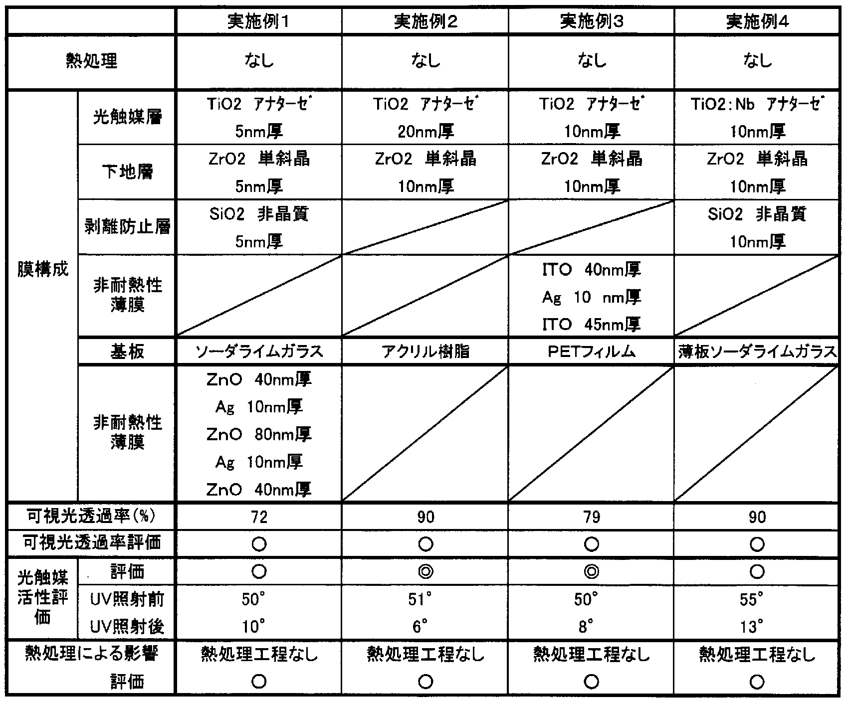
- Tables 1 and 2 below summarize the evaluation results of the non-heat-resistant thin films of Examples 14 to 14, the configurations of the underlayer, the photocatalyst layer, and the anti-peeling layer, and the photocatalytic and optical properties.
- the heat treatment step of Comparative Example 16 and the method for forming the photocatalytic layer and the peel-prevention layer, and the evaluation results of the photocatalytic properties and the optical properties are also shown.
- a zinc oxide layer and a silver layer are alternately laminated on a soda-lime glass substrate with a length of Im x width lm and a thickness of 3 mm.
- a multilayer film having a structure of 40 nm / silver layer 1 Onm / zinc oxide layer 80 nm / silver layer 1 Onm / zinc oxide layer 40 nm was formed.
- the zinc oxide layer was formed using a zinc oxide target to which aluminum was added, and the silver layer was formed using a silver target.
- Each of the layers was formed in a reduced-pressure argon atmosphere without heating.
- This multilayer film of zinc oxide and silver has a heat ray reflection function, but has low heat resistance.
- the heat resistance temperature as defined above is 150 ° C. would.
- a photocatalytic glass having a non-heat-resistant function in which a heat ray reflecting film composed of a multilayer film of zinc oxide and silver was formed on one surface of a soda lime glass substrate and a photocatalyst layer was formed on the other surface.
- a heat ray reflecting film composed of a multilayer film of zinc oxide and silver was formed on one surface of a soda lime glass substrate and a photocatalyst layer was formed on the other surface.
- silver aggregation did not occur, and an article having high visible light transmittance was obtained.
- Table 1 shows the measurement results of the visible light transmittance.
- the visible light transmittance was measured using a D65 light source according to JIS R3106 “Test method for transmittance of sheet glass 'reflectance' emissivity and solar heat gain”.
- the photocatalytic activity of the photocatalyst layer was evaluated using an index of hydrophilicity-imparting performance. After the formation of the photocatalyst layer, the multilayer film article was left in a place where no light was irradiated for 14 days, and carbon in the atmosphere was deposited on the surface to reduce the hydrophilicity of the surface. Thereafter, the surface of the titanium oxide layer was irradiated with ultraviolet light having an intensity of lmWZcm 2 for 1 hour using a black light, and the following evaluation was performed based on the contact angle of water droplets after irradiation. Water contact angle (°) Photocatalytic activity evaluation
- soda-lime glass substrate having the heat ray reflective film formed on the inner side With the soda-lime glass substrate having the heat ray reflective film formed on the inner side, another soda lime glass and this glass are subjected to a multi-layer glass processing treatment, and the heat ray reflective film is formed on the inner surface of the outdoor glass.
- a heat-reflective double-glazed glass having an antifouling function in which a photocatalyst antifouling film was formed on the outer surface of the outdoor glass was obtained.
- a monoclinic dinoreconium oxide layer lOnmZ anatase-type titanium oxide layer of 20 nm was formed on an acrylic resin substrate having a length of lm x a width of lm and a thickness of 3 mm.
- Each film was formed by a non-heated reactive sputtering method using a zirconium target and a titanium target in an atmosphere (0.93 Pa) of an equal mixture of argon and oxygen.
- the acrylic resin has low heat resistance, and the heat resistance temperature as defined above is 230 ° C. Exposure to temperatures higher than this temperature will result in a yellow coloration. Since no heating step was used in the photocatalytic layer film forming step, the acrylic resin substrate did not turn yellow, and the optical characteristics of the acrylic resin before and after the film formation did not change at all.
- This non-heat-resistant photocatalytic glass substrate can be used as a display substrate.
- an indium tin oxide (IT ⁇ ) layer and a silver layer are alternately laminated on a polyethylene terephthalate (PET) film substrate with a length of lm x a width of lm and a thickness of 3 mm.
- a multilayer film having a structure of: ⁇ layer 45 nm / silver layer 1 OnmZlTO layer 40 nm was obtained.
- the ITO layer was formed by using an ITO target, and the silver layer was formed by using a silver target without heating in a reduced-pressure argon atmosphere.
- the multilayer film of IT ⁇ and silver has a heat ray reflection function, but has low heat resistance, and the heat resistance temperature defined above is 150 ° C. When exposed to temperatures exceeding this heat resistance temperature, silver aggregates and blacks out. It will be.
- the PET film itself is also heat-resistant The temperature is 180 ° C. Above this temperature, softening deformation is remarkable.
- the PET film substrate and the silver layer contain elements having low heat resistance, but since no heating step was used in the film forming step, no deterioration was observed, and the article had good optical characteristics. was gotten.
- This photocatalyst substrate can be used as an antifouling film having an electromagnetic shielding function.
- a silicon oxide layer lOnm / monoclinic dinoreconium oxide layer 1 Onm / niobium-doped anatase-type titanium oxide layer 1 on a thin soda lime glass substrate with a length of lm x a width of lm and a thickness of lmm Onm formed.
- the silicon oxide layer and the monoclinic dinoreconium oxide layer were formed by a non-heating reactive sputtering method using a silicon target and a zirconium target, respectively, in a mixed atmosphere of argon and oxygen (0.93 Pa). Formed.
- the Nb-doped anatase-type titanium oxide layer was formed by a non-heating sputtering method in an argon atmosphere (0.93 Pa) using a titanium-niobium oxide target.
- the niobium titanium oxide layer of the obtained article had good photocatalytic activity.
- a thin soda-lime glass substrate having a thickness of lmm is easily deformed when exposed to a high temperature, and the heat-resistant temperature as defined above is 500 ° C. Since no heating step was performed in the film formation, no deformation of the substrate was observed before and after the film formation.
- This photocatalyst substrate can be used as a biochemical chip.
- Example 2 Each film was formed under the same conditions as in Example 1 except that the dinoreconium oxide layer was not formed.
- the resulting article had a high visible light transmittance of 73%, which was excellent.
- the evaluation of the photocatalytic activity of the titanium oxide layer was "X".
- the article of Comparative Example 1 was heated in the air at 400 ° C. for 30 minutes to perform a heat treatment on the titanium oxide film. After this heat treatment, the evaluation of the photocatalytic activity was “ ⁇ ”, but the visible light transmittance was reduced due to aggregation of the silver in the heat ray reflective film (from 73% before heating to 54% after heating).
- Example 2 Each film was formed under the same conditions as in Example 2 except that the dinoreconium oxide layer was not formed. As a result of evaluating the photocatalytic activity of the titanium oxide layer of the obtained article, the evaluation was "X".
- the article of Comparative Example 3 was heated in the air at 350 ° C. for 30 minutes to perform a heat treatment on the titanium oxide film. After this heat treatment, the evaluation of the photocatalytic activity was “ ⁇ ”, but the acrylic resin on the substrate turned yellow and the visible light transmittance was reduced (from 92% before heating to 75% after heating).
- Example 4 Each film was formed under the same conditions as in Example 4 except that the dinoleconium oxide layer was not formed. As a result of evaluating the photocatalytic activity of the titanium oxide layer of the obtained article, the evaluation was “X”.
- the article of Comparative Example 5 was heated in the air at 600 ° C. for 30 minutes to perform a heat treatment on the titanium oxide film. After this heat treatment, the evaluation of the photocatalytic activity was “ ⁇ ”, but it was clear that the substrate was significantly deformed and could not be used as a commercial product.
Landscapes
- Chemical & Material Sciences (AREA)
- Engineering & Computer Science (AREA)
- Materials Engineering (AREA)
- Organic Chemistry (AREA)
- Chemical Kinetics & Catalysis (AREA)
- Inorganic Chemistry (AREA)
- Mechanical Engineering (AREA)
- Metallurgy (AREA)
- Ceramic Engineering (AREA)
- Life Sciences & Earth Sciences (AREA)
- General Chemical & Material Sciences (AREA)
- Geochemistry & Mineralogy (AREA)
- Catalysts (AREA)
- Surface Treatment Of Glass (AREA)
- Physical Vapour Deposition (AREA)
Description

Claims
Priority Applications (3)
| Application Number | Priority Date | Filing Date | Title |
|---|---|---|---|
| JP2005506824A JP4460537B2 (ja) | 2003-06-09 | 2004-06-09 | 光触媒部材 |
| US10/560,053 US20070082205A1 (en) | 2003-06-09 | 2004-06-09 | Photocatalytic member |
| EP04745697A EP1637225A4 (en) | 2003-06-09 | 2004-06-09 | PHOTOCATALYST ELEMENT |
Applications Claiming Priority (2)
| Application Number | Priority Date | Filing Date | Title |
|---|---|---|---|
| JP2003164129 | 2003-06-09 | ||
| JP2003-164129 | 2003-06-09 |
Publications (1)
| Publication Number | Publication Date |
|---|---|
| WO2004108283A1 true WO2004108283A1 (ja) | 2004-12-16 |
Family
ID=33508776
Family Applications (1)
| Application Number | Title | Priority Date | Filing Date |
|---|---|---|---|
| PCT/JP2004/008022 Ceased WO2004108283A1 (ja) | 2003-06-09 | 2004-06-09 | 光触媒部材 |
Country Status (5)
| Country | Link |
|---|---|
| US (1) | US20070082205A1 (ja) |
| EP (1) | EP1637225A4 (ja) |
| JP (1) | JP4460537B2 (ja) |
| CN (1) | CN100482346C (ja) |
| WO (1) | WO2004108283A1 (ja) |
Cited By (10)
| Publication number | Priority date | Publication date | Assignee | Title |
|---|---|---|---|---|
| JP2006307623A (ja) * | 2005-03-31 | 2006-11-09 | Mitsubishi Materials Corp | 環境機能建材及びその製造方法 |
| WO2007092511A3 (en) * | 2006-02-08 | 2008-03-06 | Ppg Ind Ohio Inc | Coated substrates having undercoating layers that exhibit improved photocatalytic activity |
| WO2008047810A1 (fr) * | 2006-10-16 | 2008-04-24 | Nippon Sheet Glass Company, Limited | Substrat antibactérien et son procédé de production |
| JP2008516878A (ja) * | 2004-10-18 | 2008-05-22 | ピルキントン グループ リミテッド | 日照調整ガラス |
| US20090117371A1 (en) * | 2006-04-07 | 2009-05-07 | Interpane Entwicklungs-Und Beratungsgesellschaft Mbh & Co. Kg | Weather-resistant layer system |
| JP2012124302A (ja) * | 2010-12-08 | 2012-06-28 | Ricoh Co Ltd | 電気−機械変換膜とその作製方法、電気−機械変換素子、液体吐出ヘッドおよび液体吐出装置 |
| JP2014071292A (ja) * | 2012-09-28 | 2014-04-21 | Dainippon Printing Co Ltd | 反射防止物品 |
| JP2015112524A (ja) * | 2013-12-10 | 2015-06-22 | 大日本印刷株式会社 | 光触媒機能材料の製造方法、及び光触媒膜形成用スパッタリングターゲットの製造方法 |
| JP2016527078A (ja) * | 2013-07-05 | 2016-09-08 | 日東電工株式会社 | 透明光触媒コーティングおよびそれを製造する方法 |
| WO2018190408A1 (ja) * | 2017-04-14 | 2018-10-18 | Hoya株式会社 | 光学素子及び光学薄膜 |
Families Citing this family (22)
| Publication number | Priority date | Publication date | Assignee | Title |
|---|---|---|---|---|
| KR100956214B1 (ko) * | 2001-12-21 | 2010-05-04 | 니혼 이타가라스 가부시키가이샤 | 광촉매 기능을 갖는 부재 및 그 제조방법 |
| JP4362476B2 (ja) * | 2003-06-20 | 2009-11-11 | 日本板硝子株式会社 | 光触媒機能を有する部材および複層ガラス |
| FR2861386B1 (fr) * | 2003-10-23 | 2006-02-17 | Saint Gobain | Substrat, notamment substrat verrier, portant une couche a propriete photocatalytique revetue d'une couche mince protectrice. |
| EP1852402A1 (en) * | 2004-12-06 | 2007-11-07 | Nippon Sheet Glass Company Limited | Glass member having photocatalytic function and heat ray reflective function, and double layer glass employing it |
| US7846492B2 (en) * | 2006-04-27 | 2010-12-07 | Guardian Industries Corp. | Photocatalytic window and method of making same |
| US7892662B2 (en) | 2006-04-27 | 2011-02-22 | Guardian Industries Corp. | Window with anti-bacterial and/or anti-fungal feature and method of making same |
| US7632761B2 (en) * | 2006-06-01 | 2009-12-15 | Wayne State University | Method of making thin film anatase titanium dioxide |
| CN104279025A (zh) | 2008-05-29 | 2015-01-14 | 三井金属矿业株式会社 | 颗粒燃烧催化剂、颗粒过滤器和废气净化设备 |
| CN102471144B (zh) * | 2009-08-17 | 2014-11-05 | 日本板硝子株式会社 | 具备光催化剂膜的玻璃制品 |
| US8946112B2 (en) | 2009-10-30 | 2015-02-03 | Empire Technology Development Llc | Photocatalytic material for splitting oxides of carbon |
| FR2963343B1 (fr) * | 2010-07-28 | 2012-07-27 | Saint Gobain | Vitrage pourvu d'un revetement contre la condensation |
| KR102099726B1 (ko) * | 2012-12-04 | 2020-04-13 | 인고 스토르크 게난트 베르스보르그 | 열처리 모니터링 시스템 |
| US10611679B2 (en) | 2017-10-26 | 2020-04-07 | Guardian Glass, LLC | Coated article including noble metal and polymeric hydrogenated diamond like carbon composite material having antibacterial and photocatalytic properties, and/or methods of making the same |
| JP7422450B2 (ja) * | 2018-03-20 | 2024-01-26 | キヤノン株式会社 | 透明部材、撮像装置、透明部材の製造方法および部材 |
| US20190295391A1 (en) * | 2018-03-20 | 2019-09-26 | Canon Kabushiki Kaisha | Transparent member, imaging apparatus, and method of producing transparent member |
| US10759693B2 (en) * | 2018-07-16 | 2020-09-01 | Guardian Glass, LLC | Low-E matchable coated articles having absorber film and corresponding methods |
| US10752541B2 (en) | 2018-07-16 | 2020-08-25 | Guardian Glass, LLC | Low-E matchable coated articles having doped seed layer under silver, and corresponding methods |
| US10301215B1 (en) | 2018-07-16 | 2019-05-28 | Guardian Glass, LLC | Low-E matchable coated articles having doped seed layer under silver, and corresponding methods |
| US10787385B2 (en) * | 2018-07-16 | 2020-09-29 | Guardian Glass, LLC | Low-E matchable coated articles having absorber film and corresponding methods |
| KR102692564B1 (ko) * | 2018-09-21 | 2024-08-06 | 삼성전자주식회사 | 다층 박막 구조물 및 이를 이용한 위상 변환 소자 |
| JP2023148631A (ja) | 2022-03-30 | 2023-10-13 | デクセリアルズ株式会社 | 光触媒部材 |
| TW202513154A (zh) | 2023-09-01 | 2025-04-01 | 日商迪睿合股份有限公司 | 光觸媒構件及光觸媒構件之製造方法 |
Citations (3)
| Publication number | Priority date | Publication date | Assignee | Title |
|---|---|---|---|---|
| JPH10278165A (ja) * | 1997-04-08 | 1998-10-20 | Asahi Glass Co Ltd | 積層体の製造方法 |
| JP2002030417A (ja) * | 2000-07-14 | 2002-01-31 | Japan Atom Energy Res Inst | アナターゼ型結晶構造の酸化チタン単結晶薄膜の作製法 |
| WO2002040417A2 (en) * | 2000-08-31 | 2002-05-23 | Ppg Industries Ohio, Inc. | Methods of obtaining photoactive coatings and/or anatase crystalline phase of titanium oxides and articles made thereby |
Family Cites Families (4)
| Publication number | Priority date | Publication date | Assignee | Title |
|---|---|---|---|---|
| EP0844985A1 (en) * | 1995-08-18 | 1998-06-03 | Adam Heller | Self-cleaning glass and method of making thereof |
| FR2738813B1 (fr) * | 1995-09-15 | 1997-10-17 | Saint Gobain Vitrage | Substrat a revetement photo-catalytique |
| KR100554451B1 (ko) * | 1997-12-02 | 2006-03-03 | 쇼와 덴코 가부시키가이샤 | 광촉매성 산화물 함유 조성물, 박막 및 복합체 |
| JP4174862B2 (ja) * | 1998-08-04 | 2008-11-05 | ソニー株式会社 | 薄膜トランジスタの製造方法および半導体装置の製造方法 |
-
2004
- 2004-06-09 EP EP04745697A patent/EP1637225A4/en not_active Withdrawn
- 2004-06-09 US US10/560,053 patent/US20070082205A1/en not_active Abandoned
- 2004-06-09 WO PCT/JP2004/008022 patent/WO2004108283A1/ja not_active Ceased
- 2004-06-09 CN CNB2004800225921A patent/CN100482346C/zh not_active Expired - Fee Related
- 2004-06-09 JP JP2005506824A patent/JP4460537B2/ja not_active Expired - Fee Related
Patent Citations (3)
| Publication number | Priority date | Publication date | Assignee | Title |
|---|---|---|---|---|
| JPH10278165A (ja) * | 1997-04-08 | 1998-10-20 | Asahi Glass Co Ltd | 積層体の製造方法 |
| JP2002030417A (ja) * | 2000-07-14 | 2002-01-31 | Japan Atom Energy Res Inst | アナターゼ型結晶構造の酸化チタン単結晶薄膜の作製法 |
| WO2002040417A2 (en) * | 2000-08-31 | 2002-05-23 | Ppg Industries Ohio, Inc. | Methods of obtaining photoactive coatings and/or anatase crystalline phase of titanium oxides and articles made thereby |
Non-Patent Citations (1)
| Title |
|---|
| See also references of EP1637225A4 * |
Cited By (14)
| Publication number | Priority date | Publication date | Assignee | Title |
|---|---|---|---|---|
| JP2008516878A (ja) * | 2004-10-18 | 2008-05-22 | ピルキントン グループ リミテッド | 日照調整ガラス |
| JP2006307623A (ja) * | 2005-03-31 | 2006-11-09 | Mitsubishi Materials Corp | 環境機能建材及びその製造方法 |
| WO2007092511A3 (en) * | 2006-02-08 | 2008-03-06 | Ppg Ind Ohio Inc | Coated substrates having undercoating layers that exhibit improved photocatalytic activity |
| US20090117371A1 (en) * | 2006-04-07 | 2009-05-07 | Interpane Entwicklungs-Und Beratungsgesellschaft Mbh & Co. Kg | Weather-resistant layer system |
| WO2008047810A1 (fr) * | 2006-10-16 | 2008-04-24 | Nippon Sheet Glass Company, Limited | Substrat antibactérien et son procédé de production |
| JP2012124302A (ja) * | 2010-12-08 | 2012-06-28 | Ricoh Co Ltd | 電気−機械変換膜とその作製方法、電気−機械変換素子、液体吐出ヘッドおよび液体吐出装置 |
| JP2014071292A (ja) * | 2012-09-28 | 2014-04-21 | Dainippon Printing Co Ltd | 反射防止物品 |
| JP2016527078A (ja) * | 2013-07-05 | 2016-09-08 | 日東電工株式会社 | 透明光触媒コーティングおよびそれを製造する方法 |
| US10391482B2 (en) | 2013-07-05 | 2019-08-27 | Nitto Denko Corporation | Transparent photocatalyst coating and methods of manufacturing the same |
| US10710063B2 (en) | 2013-07-05 | 2020-07-14 | Nitto Denko Corporation | Transparent photocatalyst coating and methods of manufacturing the same |
| JP2015112524A (ja) * | 2013-12-10 | 2015-06-22 | 大日本印刷株式会社 | 光触媒機能材料の製造方法、及び光触媒膜形成用スパッタリングターゲットの製造方法 |
| WO2018190408A1 (ja) * | 2017-04-14 | 2018-10-18 | Hoya株式会社 | 光学素子及び光学薄膜 |
| JPWO2018190408A1 (ja) * | 2017-04-14 | 2020-03-05 | Hoya株式会社 | 光学素子及び光学薄膜 |
| JP7091315B2 (ja) | 2017-04-14 | 2022-06-27 | Hoya株式会社 | 光学素子及びその製造方法 |
Also Published As
| Publication number | Publication date |
|---|---|
| EP1637225A1 (en) | 2006-03-22 |
| CN100482346C (zh) | 2009-04-29 |
| US20070082205A1 (en) | 2007-04-12 |
| JPWO2004108283A1 (ja) | 2006-07-20 |
| EP1637225A4 (en) | 2007-12-19 |
| JP4460537B2 (ja) | 2010-05-12 |
| CN1832804A (zh) | 2006-09-13 |
Similar Documents
| Publication | Publication Date | Title |
|---|---|---|
| JP4460537B2 (ja) | 光触媒部材 | |
| EP1466665B1 (en) | Member having photocatalytic function and method for manufacture thereof | |
| EP1315682B1 (en) | Methods of obtaining photoactive coatings and/or anatase crystalline phase of titanium oxides and articles made thereby | |
| JP4362476B2 (ja) | 光触媒機能を有する部材および複層ガラス | |
| KR101131157B1 (ko) | 보호용 박층으로 코팅되어 있는 광촉매 층을 지지하는기판, 특히 유리 기판 | |
| CA2543075C (fr) | Substrat, notamment substrat verrier, portant au moins un empilement couche a propriete photocatalytique / sous-couche de croissance heteroepitaxiale de ladite couche | |
| EP1068899A1 (en) | Multilayer structure and process for producing the same | |
| US20080124460A1 (en) | Methods of obtaining photoactive coatings and/or anatase crystalline phase of titanium oxides and articles made thereby | |
| JP2007512154A5 (ja) | ||
| CN1747907A (zh) | 载有涂层叠层的玻璃板 | |
| RU2481364C2 (ru) | Промежуточные слои, обеспечивающие улучшенную функциональность верхнего слоя | |
| CN100465118C (zh) | 涂层的玻璃 | |
| JP2000239047A (ja) | 親水性光触媒部材 | |
| CN101072735A (zh) | 具有光催化剂功能和红外线反射功能的玻璃构件以及使用该玻璃构件的多层玻璃 | |
| US20250196104A1 (en) | Photocatalyst member | |
| JP3925179B2 (ja) | 防曇防汚物品とその製造方法 | |
| WO2025047938A1 (ja) | 光触媒部材及び光触媒部材の製造方法 | |
| JP2025036359A (ja) | 光触媒部材及び光触媒部材の製造方法 |
Legal Events
| Date | Code | Title | Description |
|---|---|---|---|
| WWE | Wipo information: entry into national phase |
Ref document number: 200480022592.1 Country of ref document: CN |
|
| WWE | Wipo information: entry into national phase |
Ref document number: 2005506824 Country of ref document: JP |
|
| AK | Designated states |
Kind code of ref document: A1 Designated state(s): AE AG AL AM AT AU AZ BA BB BG BR BW BY BZ CA CH CN CO CR CU CZ DE DK DM DZ EC EE EG ES FI GB GD GE GH GM HR HU ID IL IN IS JP KE KG KP KR KZ LC LK LR LS LT LU LV MA MD MG MK MN MW MX MZ NA NI NO NZ OM PG PH PL PT RO RU SC SD SE SG SK SL SY TJ TM TN TR TT TZ UA UG US UZ VC VN YU ZA ZM ZW |
|
| AL | Designated countries for regional patents |
Kind code of ref document: A1 Designated state(s): GM KE LS MW MZ NA SD SL SZ TZ UG ZM ZW AM AZ BY KG KZ MD RU TJ TM AT BE BG CH CY CZ DE DK EE ES FI FR GB GR HU IE IT LU MC NL PL PT RO SE SI SK TR BF BJ CF CG CI CM GA GN GQ GW ML MR NE SN TD TG |
|
| WWE | Wipo information: entry into national phase |
Ref document number: 2004745697 Country of ref document: EP |
|
| 121 | Ep: the epo has been informed by wipo that ep was designated in this application | ||
| WWP | Wipo information: published in national office |
Ref document number: 2004745697 Country of ref document: EP |
|
| WWE | Wipo information: entry into national phase |
Ref document number: 2007082205 Country of ref document: US Ref document number: 10560053 Country of ref document: US |
|
| WWP | Wipo information: published in national office |
Ref document number: 10560053 Country of ref document: US |