WO2005018284A1 - Organic el device - Google Patents
Organic el device Download PDFInfo
- Publication number
- WO2005018284A1 WO2005018284A1 PCT/KR2004/001937 KR2004001937W WO2005018284A1 WO 2005018284 A1 WO2005018284 A1 WO 2005018284A1 KR 2004001937 W KR2004001937 W KR 2004001937W WO 2005018284 A1 WO2005018284 A1 WO 2005018284A1
- Authority
- WO
- WIPO (PCT)
- Prior art keywords
- organic
- layer
- chemical formula
- hole injection
- interface
- Prior art date
- Legal status (The legal status is an assumption and is not a legal conclusion. Google has not performed a legal analysis and makes no representation as to the accuracy of the status listed.)
- Ceased
Links
Classifications
-
- H—ELECTRICITY
- H10—SEMICONDUCTOR DEVICES; ELECTRIC SOLID-STATE DEVICES NOT OTHERWISE PROVIDED FOR
- H10K—ORGANIC ELECTRIC SOLID-STATE DEVICES
- H10K50/00—Organic light-emitting devices
- H10K50/10—OLEDs or polymer light-emitting diodes [PLED]
- H10K50/17—Carrier injection layers
-
- H—ELECTRICITY
- H05—ELECTRIC TECHNIQUES NOT OTHERWISE PROVIDED FOR
- H05B—ELECTRIC HEATING; ELECTRIC LIGHT SOURCES NOT OTHERWISE PROVIDED FOR; CIRCUIT ARRANGEMENTS FOR ELECTRIC LIGHT SOURCES, IN GENERAL
- H05B33/00—Electroluminescent light sources
- H05B33/12—Light sources with substantially two-dimensional [2D] radiating surfaces
- H05B33/20—Light sources with substantially two-dimensional [2D] radiating surfaces characterised by the chemical or physical composition or the arrangement of the material in which the electroluminescent material is embedded
-
- H—ELECTRICITY
- H10—SEMICONDUCTOR DEVICES; ELECTRIC SOLID-STATE DEVICES NOT OTHERWISE PROVIDED FOR
- H10K—ORGANIC ELECTRIC SOLID-STATE DEVICES
- H10K2101/00—Properties of the organic materials covered by group H10K85/00
- H10K2101/80—Composition varying spatially, e.g. having a spatial gradient
-
- H—ELECTRICITY
- H10—SEMICONDUCTOR DEVICES; ELECTRIC SOLID-STATE DEVICES NOT OTHERWISE PROVIDED FOR
- H10K—ORGANIC ELECTRIC SOLID-STATE DEVICES
- H10K85/00—Organic materials used in the body or electrodes of devices covered by this subclass
- H10K85/60—Organic compounds having low molecular weight
- H10K85/615—Polycyclic condensed aromatic hydrocarbons, e.g. anthracene
-
- H—ELECTRICITY
- H10—SEMICONDUCTOR DEVICES; ELECTRIC SOLID-STATE DEVICES NOT OTHERWISE PROVIDED FOR
- H10K—ORGANIC ELECTRIC SOLID-STATE DEVICES
- H10K85/00—Organic materials used in the body or electrodes of devices covered by this subclass
- H10K85/60—Organic compounds having low molecular weight
- H10K85/631—Amine compounds having at least two aryl rest on at least one amine-nitrogen atom, e.g. triphenylamine
-
- Y—GENERAL TAGGING OF NEW TECHNOLOGICAL DEVELOPMENTS; GENERAL TAGGING OF CROSS-SECTIONAL TECHNOLOGIES SPANNING OVER SEVERAL SECTIONS OF THE IPC; TECHNICAL SUBJECTS COVERED BY FORMER USPC CROSS-REFERENCE ART COLLECTIONS [XRACs] AND DIGESTS
- Y10—TECHNICAL SUBJECTS COVERED BY FORMER USPC
- Y10S—TECHNICAL SUBJECTS COVERED BY FORMER USPC CROSS-REFERENCE ART COLLECTIONS [XRACs] AND DIGESTS
- Y10S428/00—Stock material or miscellaneous articles
- Y10S428/917—Electroluminescent
Definitions
- the present invention relates to an organic EL (electroluminescence) device, and more particularly, to a hole injection layer of an organic EL device.
- organic EL electroluminescence
- FIG. 1 illustrates the related art organic EL device. Firstly, as shown in FIG. 1, the anode 2 as a first electrode is formed on a transparent substrate 1. At this time, the anode 2 is formed of ITO
- HIL hole injection layer
- the HIL 3 is usually formed of copper phthalocyanine (CuPc).
- an HTL (hole transport layer) 4 is formed on the HIL 3.
- the HTL 4 is formed of
- an organic emitting layer 5 is formed on the HTL 4. At this time, a dopant may be added at needed. Then, an ETL (electron transport layer) 6 and an EIL (electron injecting layer) 7 are sequentially formed on the organic emitting layer 5.
- the EIL 7 is formed of LiF or Li 2 O. After that, the cathode 8 as a second electrode is formed on the EIL 7 so that the manufacturing process of the organic EL device is completed.
- the related art organic EL device has the following disadvantages.
- the related art organic EL device has problems of low efficiency and short life span.
- the thermal stress When driving the related art organic EL device at a high voltage current, the thermal stress generates between the anode 2 and the HIL 3. Thus, the life span of device becomes short due to the thermal stress.
- the organic material used for the HIL 3 has great motility of the hole, a hole-electron charge balance is lost so that quantum efficiency is lowered. That is, in case of the organic EL device requiring the low voltage driving, it is necessary to improve the quantum efficiency for the increase of efficiency. In this respect, the organic material used for the related art HIL is not suitable for improving the quantum efficiency.
- the present invention is directed to an organic EL device that substantially obviates one or more problems due to limitations and disadvantages of the related art.
- An object of the present invention is to provide an organic EL device to obtain great efficiency and long life span. Additional advantages, objects, and features of the invention will be set forth in part in the description which follows and in part will become apparent to those having ordinary skill in the art upon examination of the following or may be learned from practice of the invention. The objectives and other advantages of the invention may be realized and attained by the structure particularly pointed out in the written description and claims hereof as well as the appended drawings.
- an organic EL device includes an organic multilayer formed between first and second electrodes, the organic multilayer comprising a hole injection layer formed on the first electrode, and formed of a mixture of at least one selected from organic materials and at least one selected from inorganic materials; a hole transport layer having at least one layer on the hole injection layer; and an emitting layer formed on the hole transport layer. Furthermore, the organic EL device includes an electron transport layer formed on the emitting layer; and an electron injecting layer formed on the electron transport layer.
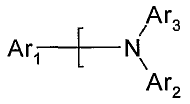
- the organic material of the hole injection layer is any one selected from Aromatic amine group. Also, the organic material of the hole injection layer is expressed as the following chemical formula 1. Chemical Formula 1
- 'n' of the chemical formula 1 is a positive number from 1 to 4, and at least any one of Arl, Ar2 and Ar3 is selected from the Aromatic group substituted or not.
- At least any one of Arl, Ar2 and Ar3 is one of phenyl, naphthyl, biphenyly, biphenylelnyl, phenanthrenyl, fluoreyl, terphenylyl and anthracenyl groups.
- a substituent of Arl, Ar2 and Ar3 is one of methyl, ethyl, propyl, t-buthyl, methoxy. ethoxy, propoxy, dimethylamine, diethylamine, phenyl, fluorin, clorine, bromine and diphenylamine groups.
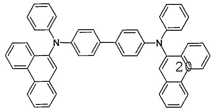
- organic material of the hole injection layer is any one of the following chemical formulas 2-7.
- Chemical Formula 2 is any one of the following chemical formulas 2-7.
- the inorganic material of the hole injection layer is formed of any one of halide compound or oxide compound selected from 1A, 2A, 3A and 4A groups of the periodic table.
- the halide compound is any one of LiF, NaF, KF, RbF, CsF and FrF
- the oxide compound is any one of Li 2 O, Na 2 O, K 2 O, BeO, MgO, CaO, B 2 O 3 , Al 2 O 3 and SiO 2 .
- the hole injection layer is formed of at least one first-layer of organic material and at least one second-layer of inorganic material, and the first and second layers are alternately deposited.
- each of the first and second layers is formed at a thickness of approx. 0.1 nm to 10 nm.
- the hole injection layer is formed at a total thickness of approx. 0J nm to
- the hole injection layer is formed of a mixture of at least one selected from organic materials and at least one selected from inorganic materials.
- the mixture has the organic material X and the inorganic material Y at the composition ratio of 1-100 to 1, or at the composition ratio of 1 to 1-100.
- the mixture has an organic material composition X value forming a gradient at a thickness direction, or an inorganic material composition Y value forming a gradient at a thickness direction.
- the hole injection layer is formed of two layers, and the respective layers are formed of different materials.
- FIG. 1 illustrates a general organic EL device
- FIG. 2 and FIG. 3 illustrate an organic EL device according to the present invention
- FIG. 4 illustrates a graph showing efficiency of an organic EL device according to the present invention.
- FIG. 5 illustrates a graph showing life span of an organic EL device according to the present invention.
- FIG. 2 and FIG. 3 illustrate the organic EL device according to the present invention.
- the anode 12 as a first electrode is formed on a transparent substrate 11.
- the anode 12 is formed of ITO (indium-tin-oxide).
- an HIL (hole injection layer) 13 is formed on the anode 12.
- the HIL 13 is formed of a mixture of at least one selected from organic materials and at least one selected from inorganic materials.
- the organic material of the HIL 13 is any one selected from Aromatic amine group, which is expressed as following chemical formula 1,
- 'n' is a positive number from 1 to 4, and at least any one of Arl, Ar2 and Ar3 is selected from the aromatic group substituted or not).
- Arl, Ar2 and Ar3 may be one of phenyl, naphthyl, biphenyly, biphenylelnyl, phenanthrenyl, fluoreyl, terphenylyl and anthracenyl groups.
- a substituent of Arl, Ar2 and Ar3 may be one of methyl, ethyl, propyl, t-buthyl, methoxy, ethoxy, propoxy, dimethylamine, diethylamine, phenyl, fiuorin, clorine, bromine and diphenylamine groups.
- the HIL 13 may be any one of the following chemical formulas 2-7. Chemical Formula 2
- the HIL 13 may be formed of any one of halide compound or oxide compound selected from 1A, 2 A, 3 A and 4A groups of the periodic table.
- the halide compound may be LiF, NaF, KF, RbF, CsF or FrF.
- the oxide compound may be Li 2 O, Na 2 O, K 2 O, BeO, MgO, CaO, B 2 O 3 , Al 2 O 3 or SiO 2 .
- the HIL 13 may be formed of at least one first-layer of an organic material, and at least one second-layer of an inorganic material.
- the first and second layers are alternately deposited.
- each of the first and second layers is formed at a thickness of approx. 0J nm to 10 nm.
- the HIL 13 is formed at a total thickness of approx. 0J nm to 300 nm.
- the HIL 13 may be formed of a mixture of at least one selected from organic materials and at least one selected from inorganic materials. That is, the HIL 13 is formed in a method of mixing the organic and inorganic materials by co-deposition. In this case, the inorganic material is at 1-90% of the mixture. At this time, the HIL 13 is maintained at the total thickness of approx. 0.1 ran to 300 nm.
- an organic material composition X value may have a gradient at a thickness direction
- the HIL 13 is formed of the mixture of the organic and inorganic materials.
- the organic material of the HIL 13 is used of NPD(4,4'-bis[N-(l-naphthyl)-N-phenyl-amino]biphenyl), and the inorganic material of the HIL 13 is used of LiF.
- the composition ratio of NPD to LiF is 5 to 1.
- the HIL 13 is formed at a thickness of approx. 30 nm.
- the HTL 14 is formed on the HIL 13.
- the HTL 14 is formed of N,N'-diphenyl- N,N'-bis(3-methylphenyl)-(l,l'biphenyl)-4,4'-diamine(TPD) or 4,4'-bis[N-(l-naphthyl)-N- phenyl -aminojbiphenyl (NPD).
- the HTL 14 may be formed in a dual- layered structure having first and second HTLs 14a and 14b.
- the HTL 14 may be formed in a single-layered structure. If the HTL 14 has the two layers, the respective layers are formed of different materials.
- the first HTL 14a is formed of NPD (4,4'- bis[N-(l-naphthyl)-N-phenyl-amino]biphenyl) at a thickness of approx. 35 nm.
- the second HTL 14b is formed of NPD ((4,4'-bis[N-(l-naphthyl)-N-phenyl-amino]biphenyl) at a thickness of approx. 40 nm.
- an organic emitting layer 15 is formed on the HTL 14 at a thickness of approx. 25 nm. In this case, a dopant may be added at needed.
- Coumine derivative (C545T) is doped to Alq3(8-hydroxyquinoline aluminum) at approx. 1%.
- an ETL (electron transport layer) 16 and an EIL (electron injecting layer) 17 are sequentially formed on the organic emitting layer 15.
- the ETL is formed of Alq3(8- hydroxyquinoline aluminum) at a thickness of approx. 35 nm
- the EIL 17 is formed of LiF at a thickness of approx. 0.5 nm.
- the ETL 16 and EIL 17 may be omitted according to the type of device.
- the cathode 18 as a second electrode is formed on the EIL 17, thereby manufacturing the organic EL device.
- FIG. 4 illustrates a graph comparing efficiency of an organic EL device according to the present invention with that according to the related art
- FIG. 5 illustrates a graph showing life span of an organic EL device according to the present invention with that according to the related art.
- HIL hole injection layer
- the brightness of the present invention is greater than that of the related art at the same current density (mA/cn ).
- the operation time period of the present invention is longer than that of the related art at the current density of 50mA/cu .
- the present invention obtains quantum efficiency of approx. 21Jcd/A, and the related art obtains quantum efficiency of approx. 13.7cd/A.
- the present invention When comparing life span of the organic EL device on condition of 50mA/cd 2 , the present invention obtains the operation time period of approx. 100 hours, and the related art obtains the operation time period of approx. 40hours.
- the organic EL device according to the present invention has the following advantages.
- the organic EL device according to the present invention it is possible to obtain great luminosity and long life span thereof by decreasing the thermal stress between the anode and the
- the hole-electron charge balance is maintained so that it is possible to improve the quantum efficiency, thereby improving efficiency of the organic EL device.
Landscapes
- Physics & Mathematics (AREA)
- Optics & Photonics (AREA)
- Electroluminescent Light Sources (AREA)
Abstract
Description




Claims


Priority Applications (3)
| Application Number | Priority Date | Filing Date | Title |
|---|---|---|---|
| JP2006523121A JP4487269B2 (en) | 2003-08-14 | 2004-08-02 | Organic EL device |
| DE602004009701T DE602004009701T2 (en) | 2003-08-14 | 2004-08-02 | ORGANIC EL-INSTALLATION |
| EP04748504A EP1665896B1 (en) | 2003-08-14 | 2004-08-02 | Organic el device |
Applications Claiming Priority (2)
| Application Number | Priority Date | Filing Date | Title |
|---|---|---|---|
| KR1020030056517A KR20050015902A (en) | 2003-08-14 | 2003-08-14 | Organic electroluminescence device and fabrication method of the same |
| KR10-2003-0056517 | 2003-08-14 |
Publications (1)
| Publication Number | Publication Date |
|---|---|
| WO2005018284A1 true WO2005018284A1 (en) | 2005-02-24 |
Family
ID=36242198
Family Applications (1)
| Application Number | Title | Priority Date | Filing Date |
|---|---|---|---|
| PCT/KR2004/001937 Ceased WO2005018284A1 (en) | 2003-08-14 | 2004-08-02 | Organic el device |
Country Status (9)
| Country | Link |
|---|---|
| US (3) | US7297417B2 (en) |
| EP (1) | EP1665896B1 (en) |
| JP (1) | JP4487269B2 (en) |
| KR (2) | KR20050015902A (en) |
| CN (1) | CN100502611C (en) |
| AT (1) | ATE376762T1 (en) |
| DE (1) | DE602004009701T2 (en) |
| ES (1) | ES2295890T3 (en) |
| WO (1) | WO2005018284A1 (en) |
Cited By (3)
| Publication number | Priority date | Publication date | Assignee | Title |
|---|---|---|---|---|
| US7667389B2 (en) | 2004-12-06 | 2010-02-23 | Semiconductor Energy Laboratory Co., Ltd. | Light emitting element, light emitting device, and electronic device |
| EP1603174A3 (en) * | 2004-06-03 | 2011-03-30 | LG Display Co., Ltd. | Organic electroluminescent device |
| JP2015092578A (en) * | 2005-02-28 | 2015-05-14 | 株式会社半導体エネルギー研究所 | Composite material |
Families Citing this family (39)
| Publication number | Priority date | Publication date | Assignee | Title |
|---|---|---|---|---|
| AU2003292826A1 (en) * | 2003-12-25 | 2005-07-21 | Fujitsu Limited | Organic el element, organic el display, process for fabricating organic el element, and system for fabricating organic el element |
| KR101267040B1 (en) * | 2004-12-06 | 2013-05-23 | 가부시키가이샤 한도오따이 에네루기 켄큐쇼 | Light-emitting element and light-emitting device using the composite compound, and manufacturing method of the light-emitting element |
| KR101030008B1 (en) * | 2004-12-31 | 2011-04-20 | 삼성모바일디스플레이주식회사 | Organic electroluminescent element |
| US9530968B2 (en) * | 2005-02-15 | 2016-12-27 | Semiconductor Energy Laboratory Co., Ltd. | Light emitting element and light emitting device |
| JP5116992B2 (en) * | 2005-05-27 | 2013-01-09 | 富士フイルム株式会社 | Organic EL device |
| US8729795B2 (en) | 2005-06-30 | 2014-05-20 | Semiconductor Energy Laboratory Co., Ltd. | Light emitting device and electronic device |
| US8659008B2 (en) * | 2005-07-08 | 2014-02-25 | Semiconductor Energy Laboratory Co., Ltd. | Composite material and light emitting element, light emitting device, and electronic device using the composite material |
| JP4770492B2 (en) * | 2006-02-02 | 2011-09-14 | セイコーエプソン株式会社 | Light emitting device and manufacturing method thereof |
| KR100841369B1 (en) | 2006-12-18 | 2008-06-26 | 삼성에스디아이 주식회사 | Organic light emitting display device and manufacturing method |
| KR100805700B1 (en) * | 2006-12-29 | 2008-02-21 | 삼성에스디아이 주식회사 | Organic electronic device and manufacturing method thereof |
| US20080238300A1 (en) * | 2007-04-02 | 2008-10-02 | Sang Tae Park | Organic electroluminescence device and method for fabricating the same |
| JP5102533B2 (en) * | 2007-04-24 | 2012-12-19 | パナソニック株式会社 | Organic light emitting device |
| KR101457681B1 (en) * | 2007-09-21 | 2014-11-03 | 엘지디스플레이 주식회사 | Electroluminescent element |
| KR100879476B1 (en) * | 2007-09-28 | 2009-01-20 | 삼성모바일디스플레이주식회사 | Organic light emitting device |
| KR20090050369A (en) | 2007-11-15 | 2009-05-20 | 삼성모바일디스플레이주식회사 | Organic light emitting device |
| KR100918401B1 (en) | 2007-12-24 | 2009-09-24 | 삼성모바일디스플레이주식회사 | Organic light emitting device |
| KR100894066B1 (en) * | 2007-12-28 | 2009-04-24 | 삼성모바일디스플레이 주식회사 | Organic light emitting device |
| KR100922755B1 (en) * | 2007-12-28 | 2009-10-21 | 삼성모바일디스플레이주식회사 | Organic light emitting device |
| CN101940065A (en) * | 2008-01-23 | 2011-01-05 | Lg化学株式会社 | Organic light emitting device and method of manufacturing the same |
| KR100922759B1 (en) * | 2008-02-26 | 2009-10-21 | 삼성모바일디스플레이주식회사 | Organic light emitting device |
| KR100922760B1 (en) * | 2008-03-03 | 2009-10-21 | 삼성모바일디스플레이주식회사 | Organic light emitting device |
| KR100898075B1 (en) | 2008-03-04 | 2009-05-18 | 삼성모바일디스플레이주식회사 | Organic light emitting device |
| KR101341012B1 (en) * | 2008-08-29 | 2013-12-13 | 엘지디스플레이 주식회사 | Organic luminescence dispaly panel |
| JP2009010415A (en) * | 2008-08-29 | 2009-01-15 | Bando Chem Ind Ltd | Organic electroluminescence device |
| KR101887237B1 (en) * | 2011-08-29 | 2018-08-10 | 엘지디스플레이 주식회사 | Organic Light Emitting Display Device |
| CN103050641B (en) * | 2011-10-14 | 2016-03-02 | 乐金显示有限公司 | The display panel of organic luminescent device and this device of use |
| EP2787548A4 (en) * | 2011-11-28 | 2015-07-01 | Oceans King Lighting Science | Organic electroluminescent device having ternary doped hole transportation layer and preparation method therefor |
| JP6174877B2 (en) | 2013-03-21 | 2017-08-02 | 株式会社半導体エネルギー研究所 | Display device and electronic device |
| JP6114592B2 (en) | 2013-03-21 | 2017-04-12 | 株式会社半導体エネルギー研究所 | Display device, manufacturing method thereof, and electronic apparatus |
| CN105378964B (en) * | 2013-07-12 | 2018-01-09 | 保土谷化学工业株式会社 | Organic Electroluminescent Devices |
| JP6788335B2 (en) | 2014-08-11 | 2020-11-25 | 三星ディスプレイ株式會社Samsung Display Co.,Ltd. | Monoamine materials for organic electroluminescence devices and organic electroluminescence devices using them |
| US11322705B2 (en) * | 2015-04-17 | 2022-05-03 | Samsung Display Co., Ltd. | Organic light-emitting device |
| KR102504124B1 (en) * | 2015-07-31 | 2023-02-28 | 삼성디스플레이 주식회사 | Organic light emitting device |
| CN108198954B (en) * | 2016-12-08 | 2019-10-25 | 昆山国显光电有限公司 | Organic electroluminescent device, its manufacturing method, and display device |
| WO2019220283A1 (en) | 2018-05-18 | 2019-11-21 | 株式会社半導体エネルギー研究所 | Light-emitting element, light-emitting device, electronic device, and illumination device |
| KR102761519B1 (en) | 2020-02-26 | 2025-02-04 | 삼성디스플레이 주식회사 | Organic light emitting device |
| WO2021201621A1 (en) * | 2020-04-01 | 2021-10-07 | 경희대학교산학협력단 | Organic light-emitting diode comprising nano-island structure and method for manufacturing same |
| KR102857110B1 (en) | 2020-06-23 | 2025-09-10 | 삼성디스플레이 주식회사 | Light emitting device and electronic device including the same |
| KR102922671B1 (en) | 2020-08-28 | 2026-02-03 | 주식회사 엘지화학 | Novel compound, coating composition comprising same, organic light emitting device using same and method of manufacturing same |
Citations (4)
| Publication number | Priority date | Publication date | Assignee | Title |
|---|---|---|---|---|
| JPH10149883A (en) * | 1996-11-20 | 1998-06-02 | Sanyo Electric Co Ltd | Organic electroluminescence device |
| EP1096835A1 (en) * | 1999-03-17 | 2001-05-02 | TDK Corporation | Organic el device |
| JP2001233882A (en) * | 2000-02-28 | 2001-08-28 | Yasuhiko Shirota | Electroluminescence element |
| JP2002356463A (en) * | 2002-02-06 | 2002-12-13 | Bando Chem Ind Ltd | Liquid crystal display |
Family Cites Families (24)
| Publication number | Priority date | Publication date | Assignee | Title |
|---|---|---|---|---|
| JP3249297B2 (en) * | 1994-07-14 | 2002-01-21 | 三洋電機株式会社 | Organic electroluminescent device |
| EP0907304B1 (en) * | 1996-05-29 | 2002-11-06 | Idemitsu Kosan Company Limited | Organic el device |
| JPH11251067A (en) | 1998-03-02 | 1999-09-17 | Junji Kido | Organic electroluminescent device |
| US6486601B1 (en) * | 1998-06-26 | 2002-11-26 | Idemitsu Kosan Co., Ltd. | Organic luminescence device with reduced leakage current |
| JP3915256B2 (en) | 1998-06-29 | 2007-05-16 | 東洋インキ製造株式会社 | Organic electroluminescent device material and organic electroluminescent device using the same |
| JP2000040590A (en) | 1998-07-22 | 2000-02-08 | Tdk Corp | Organic el element |
| JP2000196140A (en) * | 1998-12-28 | 2000-07-14 | Sharp Corp | Organic electroluminescent device and manufacturing method thereof |
| JP2000252074A (en) * | 1998-12-29 | 2000-09-14 | Tdk Corp | Organic EL device |
| JP3125777B2 (en) * | 1999-01-28 | 2001-01-22 | 日本電気株式会社 | Organic electroluminescence device and panel |
| JP4560927B2 (en) | 2000-09-22 | 2010-10-13 | 住友化学株式会社 | Organic electroluminescence device |
| SG2009086778A (en) * | 2000-12-28 | 2016-11-29 | Semiconductor Energy Lab Co Ltd | Luminescent device |
| JP4076769B2 (en) | 2000-12-28 | 2008-04-16 | 株式会社半導体エネルギー研究所 | Light emitting device and electric appliance |
| US6614175B2 (en) * | 2001-01-26 | 2003-09-02 | Xerox Corporation | Organic light emitting devices |
| US6565996B2 (en) * | 2001-06-06 | 2003-05-20 | Eastman Kodak Company | Organic light-emitting device having a color-neutral dopant in a hole-transport layer and/or in an electron-transport layer |
| US6627333B2 (en) * | 2001-08-15 | 2003-09-30 | Eastman Kodak Company | White organic light-emitting devices with improved efficiency |
| US6852997B2 (en) * | 2001-10-30 | 2005-02-08 | Semiconductor Energy Laboratory Co., Ltd. | Light emitting device |
| TW511304B (en) * | 2001-12-11 | 2002-11-21 | Ind Tech Res Inst | Organic electroluminescent device with fluorine-containing inorganic layer |
| KR100474891B1 (en) | 2001-12-20 | 2005-03-08 | 엘지전자 주식회사 | organic electroluminescent display device |
| US6692846B2 (en) * | 2002-06-20 | 2004-02-17 | Eastman Kodak Company | Organic electroluminescent device having a stabilizing dopant in a hole-transport layer or in an electron-transport layer distant from the emission layer |
| JP2004079301A (en) * | 2002-08-14 | 2004-03-11 | Fuji Photo Film Co Ltd | LIGHT EMITTING ELEMENT AND MANUFACTURING METHOD THEREOF |
| US6967062B2 (en) * | 2003-03-19 | 2005-11-22 | Eastman Kodak Company | White light-emitting OLED device having a blue light-emitting layer doped with an electron-transporting or a hole-transporting material or both |
| US7037601B2 (en) * | 2003-05-28 | 2006-05-02 | Eastman Kodak Company | White light-emitting device structures |
| US6919140B2 (en) * | 2003-07-10 | 2005-07-19 | Eastman Kodak Company | Organic electroluminescent devices with high luminance |
| US20060019116A1 (en) * | 2004-07-22 | 2006-01-26 | Eastman Kodak Company | White electroluminescent device with anthracene derivative host |
-
2003
- 2003-08-14 KR KR1020030056517A patent/KR20050015902A/en not_active Abandoned
-
2004
- 2004-08-02 ES ES04748504T patent/ES2295890T3/en not_active Expired - Lifetime
- 2004-08-02 KR KR1020067002967A patent/KR100820830B1/en not_active Expired - Fee Related
- 2004-08-02 EP EP04748504A patent/EP1665896B1/en not_active Expired - Lifetime
- 2004-08-02 WO PCT/KR2004/001937 patent/WO2005018284A1/en not_active Ceased
- 2004-08-02 CN CNB2004800233773A patent/CN100502611C/en not_active Expired - Fee Related
- 2004-08-02 JP JP2006523121A patent/JP4487269B2/en not_active Expired - Fee Related
- 2004-08-02 AT AT04748504T patent/ATE376762T1/en not_active IP Right Cessation
- 2004-08-02 DE DE602004009701T patent/DE602004009701T2/en not_active Expired - Lifetime
- 2004-08-04 US US10/910,341 patent/US7297417B2/en not_active Expired - Lifetime
-
2007
- 2007-09-26 US US11/861,595 patent/US7485377B2/en not_active Expired - Lifetime
-
2008
- 2008-12-23 US US12/342,746 patent/US8512876B2/en not_active Expired - Fee Related
Patent Citations (4)
| Publication number | Priority date | Publication date | Assignee | Title |
|---|---|---|---|---|
| JPH10149883A (en) * | 1996-11-20 | 1998-06-02 | Sanyo Electric Co Ltd | Organic electroluminescence device |
| EP1096835A1 (en) * | 1999-03-17 | 2001-05-02 | TDK Corporation | Organic el device |
| JP2001233882A (en) * | 2000-02-28 | 2001-08-28 | Yasuhiko Shirota | Electroluminescence element |
| JP2002356463A (en) * | 2002-02-06 | 2002-12-13 | Bando Chem Ind Ltd | Liquid crystal display |
Cited By (3)
| Publication number | Priority date | Publication date | Assignee | Title |
|---|---|---|---|---|
| EP1603174A3 (en) * | 2004-06-03 | 2011-03-30 | LG Display Co., Ltd. | Organic electroluminescent device |
| US7667389B2 (en) | 2004-12-06 | 2010-02-23 | Semiconductor Energy Laboratory Co., Ltd. | Light emitting element, light emitting device, and electronic device |
| JP2015092578A (en) * | 2005-02-28 | 2015-05-14 | 株式会社半導体エネルギー研究所 | Composite material |
Also Published As
| Publication number | Publication date |
|---|---|
| JP2007502535A (en) | 2007-02-08 |
| KR20060133521A (en) | 2006-12-26 |
| DE602004009701D1 (en) | 2007-12-06 |
| CN100502611C (en) | 2009-06-17 |
| CN1836470A (en) | 2006-09-20 |
| EP1665896B1 (en) | 2007-10-24 |
| US20080014462A1 (en) | 2008-01-17 |
| KR20050015902A (en) | 2005-02-21 |
| US7297417B2 (en) | 2007-11-20 |
| US20090115329A1 (en) | 2009-05-07 |
| DE602004009701T2 (en) | 2008-06-05 |
| US7485377B2 (en) | 2009-02-03 |
| JP4487269B2 (en) | 2010-06-23 |
| EP1665896A1 (en) | 2006-06-07 |
| ATE376762T1 (en) | 2007-11-15 |
| US8512876B2 (en) | 2013-08-20 |
| US20050037234A1 (en) | 2005-02-17 |
| KR100820830B1 (en) | 2008-04-11 |
| ES2295890T3 (en) | 2008-04-16 |
Similar Documents
| Publication | Publication Date | Title |
|---|---|---|
| EP1665896B1 (en) | Organic el device | |
| US6150043A (en) | OLEDs containing thermally stable glassy organic hole transporting materials | |
| JP4116398B2 (en) | Organic element | |
| JP5231188B2 (en) | Organic electroluminescence device | |
| KR100650046B1 (en) | High efficiency organic EL device | |
| EP1227527A2 (en) | Organic light emitting devices | |
| CN1866536A (en) | Stacked OLED structure | |
| EP2456617A1 (en) | Oled device with stabilized yellow light-emitting layer | |
| US8274212B2 (en) | Organic light emitting device including first hole injection layer and second hole injection layer | |
| JP2003157980A (en) | Organic green light emitting element | |
| KR100879476B1 (en) | Organic light emitting device | |
| CN100544057C (en) | White organic light emitting device | |
| WO2011148801A1 (en) | Organic el element | |
| EP1603174B1 (en) | Organic electroluminescent device | |
| KR100898075B1 (en) | Organic light emitting device | |
| JP2003282265A (en) | Organic electroluminescent device | |
| EP1009042A2 (en) | Electroliuminescent device with arylethylene derivatives in hole transport layer | |
| KR100786292B1 (en) | Organic electroluminescent element | |
| JP2000150161A (en) | Organic electroluminescence display device | |
| KR100770247B1 (en) | High Efficiency Organic Electroluminescent Device | |
| JP2004031211A (en) | Organic electroluminescent device | |
| CN100481572C (en) | Tandem type organic electroluminescent assembly and application thereof | |
| JP2003168563A (en) | Organic electroluminescence device |
Legal Events
| Date | Code | Title | Description |
|---|---|---|---|
| WWE | Wipo information: entry into national phase |
Ref document number: 200480023377.3 Country of ref document: CN |
|
| AK | Designated states |
Kind code of ref document: A1 Designated state(s): AE AG AL AM AT AU AZ BA BB BG BR BW BY BZ CA CH CN CO CR CU CZ DE DK DM DZ EC EE EG ES FI GB GD GE GH GM HR HU ID IL IN IS JP KE KG KP KR KZ LC LK LR LS LT LU LV MA MD MG MK MN MW MX MZ NA NI NO NZ OM PG PH PL PT RO RU SC SD SE SG SK SL SY TJ TM TN TR TT TZ UA UG US UZ VC VN YU ZA ZM ZW |
|
| AL | Designated countries for regional patents |
Kind code of ref document: A1 Designated state(s): BW GH GM KE LS MW MZ NA SD SL SZ TZ UG ZM ZW AM AZ BY KG KZ MD RU TJ TM AT BE BG CH CY CZ DE DK EE ES FI FR GB GR HU IE IT LU MC NL PL PT RO SE SI SK TR BF BJ CF CG CI CM GA GN GQ GW ML MR NE SN TD TG |
|
| 121 | Ep: the epo has been informed by wipo that ep was designated in this application | ||
| WWE | Wipo information: entry into national phase |
Ref document number: 1020067002967 Country of ref document: KR |
|
| WWE | Wipo information: entry into national phase |
Ref document number: 2004748504 Country of ref document: EP Ref document number: 2006523121 Country of ref document: JP |
|
| WWP | Wipo information: published in national office |
Ref document number: 2004748504 Country of ref document: EP |
|
| WWP | Wipo information: published in national office |
Ref document number: 1020067002967 Country of ref document: KR |
|
| WWG | Wipo information: grant in national office |
Ref document number: 2004748504 Country of ref document: EP |