WO2005089027A1 - 有機エレクトロルミネッセンス素子用材料及びそれを用いた有機エレクトロルミネッセンス素子 - Google Patents
有機エレクトロルミネッセンス素子用材料及びそれを用いた有機エレクトロルミネッセンス素子 Download PDFInfo
- Publication number
- WO2005089027A1 WO2005089027A1 PCT/JP2005/004417 JP2005004417W WO2005089027A1 WO 2005089027 A1 WO2005089027 A1 WO 2005089027A1 JP 2005004417 W JP2005004417 W JP 2005004417W WO 2005089027 A1 WO2005089027 A1 WO 2005089027A1
- Authority
- WO
- WIPO (PCT)
- Prior art keywords
- group
- organic
- organic electroluminescent
- general formula
- layer
- Prior art date
- Legal status (The legal status is an assumption and is not a legal conclusion. Google has not performed a legal analysis and makes no representation as to the accuracy of the status listed.)
- Ceased
Links
Classifications
-
- C—CHEMISTRY; METALLURGY
- C07—ORGANIC CHEMISTRY
- C07D—HETEROCYCLIC COMPOUNDS
- C07D209/00—Heterocyclic compounds containing five-membered rings, condensed with other rings, with one nitrogen atom as the only ring hetero atom
- C07D209/56—Ring systems containing three or more rings
- C07D209/80—[b, c]- or [b, d]-condensed
- C07D209/82—Carbazoles; Hydrogenated carbazoles
- C07D209/86—Carbazoles; Hydrogenated carbazoles with only hydrogen atoms, hydrocarbon or substituted hydrocarbon radicals, directly attached to carbon atoms of the ring system
-
- C—CHEMISTRY; METALLURGY
- C09—DYES; PAINTS; POLISHES; NATURAL RESINS; ADHESIVES; COMPOSITIONS NOT OTHERWISE PROVIDED FOR; APPLICATIONS OF MATERIALS NOT OTHERWISE PROVIDED FOR
- C09K—MATERIALS FOR MISCELLANEOUS APPLICATIONS, NOT PROVIDED FOR ELSEWHERE
- C09K11/00—Luminescent materials, e.g. electroluminescent or chemiluminescent
- C09K11/06—Luminescent materials, e.g. electroluminescent or chemiluminescent containing organic luminescent materials
-
- H—ELECTRICITY
- H05—ELECTRIC TECHNIQUES NOT OTHERWISE PROVIDED FOR
- H05B—ELECTRIC HEATING; ELECTRIC LIGHT SOURCES NOT OTHERWISE PROVIDED FOR; CIRCUIT ARRANGEMENTS FOR ELECTRIC LIGHT SOURCES, IN GENERAL
- H05B33/00—Electroluminescent light sources
- H05B33/12—Light sources with substantially two-dimensional [2D] radiating surfaces
- H05B33/14—Light sources with substantially two-dimensional [2D] radiating surfaces characterised by the chemical or physical composition or the arrangement of the electroluminescent material, or by the simultaneous addition of the electroluminescent material in or onto the light source
-
- H—ELECTRICITY
- H10—SEMICONDUCTOR DEVICES; ELECTRIC SOLID-STATE DEVICES NOT OTHERWISE PROVIDED FOR
- H10K—ORGANIC ELECTRIC SOLID-STATE DEVICES
- H10K85/00—Organic materials used in the body or electrodes of devices covered by this subclass
- H10K85/60—Organic compounds having low molecular weight
- H10K85/649—Aromatic compounds comprising a hetero atom
- H10K85/657—Polycyclic condensed heteroaromatic hydrocarbons
-
- C—CHEMISTRY; METALLURGY
- C09—DYES; PAINTS; POLISHES; NATURAL RESINS; ADHESIVES; COMPOSITIONS NOT OTHERWISE PROVIDED FOR; APPLICATIONS OF MATERIALS NOT OTHERWISE PROVIDED FOR
- C09K—MATERIALS FOR MISCELLANEOUS APPLICATIONS, NOT PROVIDED FOR ELSEWHERE
- C09K2211/00—Chemical nature of organic luminescent or tenebrescent compounds
- C09K2211/10—Non-macromolecular compounds
- C09K2211/1003—Carbocyclic compounds
- C09K2211/1007—Non-condensed systems
-
- C—CHEMISTRY; METALLURGY
- C09—DYES; PAINTS; POLISHES; NATURAL RESINS; ADHESIVES; COMPOSITIONS NOT OTHERWISE PROVIDED FOR; APPLICATIONS OF MATERIALS NOT OTHERWISE PROVIDED FOR
- C09K—MATERIALS FOR MISCELLANEOUS APPLICATIONS, NOT PROVIDED FOR ELSEWHERE
- C09K2211/00—Chemical nature of organic luminescent or tenebrescent compounds
- C09K2211/10—Non-macromolecular compounds
- C09K2211/1003—Carbocyclic compounds
- C09K2211/1011—Condensed systems
-
- C—CHEMISTRY; METALLURGY
- C09—DYES; PAINTS; POLISHES; NATURAL RESINS; ADHESIVES; COMPOSITIONS NOT OTHERWISE PROVIDED FOR; APPLICATIONS OF MATERIALS NOT OTHERWISE PROVIDED FOR
- C09K—MATERIALS FOR MISCELLANEOUS APPLICATIONS, NOT PROVIDED FOR ELSEWHERE
- C09K2211/00—Chemical nature of organic luminescent or tenebrescent compounds
- C09K2211/10—Non-macromolecular compounds
- C09K2211/1003—Carbocyclic compounds
- C09K2211/1014—Carbocyclic compounds bridged by heteroatoms, e.g. N, P, Si or B
-
- C—CHEMISTRY; METALLURGY
- C09—DYES; PAINTS; POLISHES; NATURAL RESINS; ADHESIVES; COMPOSITIONS NOT OTHERWISE PROVIDED FOR; APPLICATIONS OF MATERIALS NOT OTHERWISE PROVIDED FOR
- C09K—MATERIALS FOR MISCELLANEOUS APPLICATIONS, NOT PROVIDED FOR ELSEWHERE
- C09K2211/00—Chemical nature of organic luminescent or tenebrescent compounds
- C09K2211/10—Non-macromolecular compounds
- C09K2211/1018—Heterocyclic compounds
- C09K2211/1025—Heterocyclic compounds characterised by ligands
- C09K2211/1029—Heterocyclic compounds characterised by ligands containing one nitrogen atom as the heteroatom
-
- C—CHEMISTRY; METALLURGY
- C09—DYES; PAINTS; POLISHES; NATURAL RESINS; ADHESIVES; COMPOSITIONS NOT OTHERWISE PROVIDED FOR; APPLICATIONS OF MATERIALS NOT OTHERWISE PROVIDED FOR
- C09K—MATERIALS FOR MISCELLANEOUS APPLICATIONS, NOT PROVIDED FOR ELSEWHERE
- C09K2211/00—Chemical nature of organic luminescent or tenebrescent compounds
- C09K2211/10—Non-macromolecular compounds
- C09K2211/1018—Heterocyclic compounds
- C09K2211/1025—Heterocyclic compounds characterised by ligands
- C09K2211/1092—Heterocyclic compounds characterised by ligands containing sulfur as the only heteroatom
-
- C—CHEMISTRY; METALLURGY
- C09—DYES; PAINTS; POLISHES; NATURAL RESINS; ADHESIVES; COMPOSITIONS NOT OTHERWISE PROVIDED FOR; APPLICATIONS OF MATERIALS NOT OTHERWISE PROVIDED FOR
- C09K—MATERIALS FOR MISCELLANEOUS APPLICATIONS, NOT PROVIDED FOR ELSEWHERE
- C09K2211/00—Chemical nature of organic luminescent or tenebrescent compounds
- C09K2211/18—Metal complexes
- C09K2211/185—Metal complexes of the platinum group, i.e. Os, Ir, Pt, Ru, Rh or Pd
-
- C—CHEMISTRY; METALLURGY
- C09—DYES; PAINTS; POLISHES; NATURAL RESINS; ADHESIVES; COMPOSITIONS NOT OTHERWISE PROVIDED FOR; APPLICATIONS OF MATERIALS NOT OTHERWISE PROVIDED FOR
- C09K—MATERIALS FOR MISCELLANEOUS APPLICATIONS, NOT PROVIDED FOR ELSEWHERE
- C09K2211/00—Chemical nature of organic luminescent or tenebrescent compounds
- C09K2211/18—Metal complexes
- C09K2211/186—Metal complexes of the light metals other than alkali metals and alkaline earth metals, i.e. Be, Al or Mg
-
- C—CHEMISTRY; METALLURGY
- C09—DYES; PAINTS; POLISHES; NATURAL RESINS; ADHESIVES; COMPOSITIONS NOT OTHERWISE PROVIDED FOR; APPLICATIONS OF MATERIALS NOT OTHERWISE PROVIDED FOR
- C09K—MATERIALS FOR MISCELLANEOUS APPLICATIONS, NOT PROVIDED FOR ELSEWHERE
- C09K2211/00—Chemical nature of organic luminescent or tenebrescent compounds
- C09K2211/18—Metal complexes
- C09K2211/188—Metal complexes of other metals not provided for in one of the previous groups
-
- H—ELECTRICITY
- H10—SEMICONDUCTOR DEVICES; ELECTRIC SOLID-STATE DEVICES NOT OTHERWISE PROVIDED FOR
- H10K—ORGANIC ELECTRIC SOLID-STATE DEVICES
- H10K50/00—Organic light-emitting devices
- H10K50/10—OLEDs or polymer light-emitting diodes [PLED]
- H10K50/11—OLEDs or polymer light-emitting diodes [PLED] characterised by the electroluminescent [EL] layers
-
- H—ELECTRICITY
- H10—SEMICONDUCTOR DEVICES; ELECTRIC SOLID-STATE DEVICES NOT OTHERWISE PROVIDED FOR
- H10K—ORGANIC ELECTRIC SOLID-STATE DEVICES
- H10K85/00—Organic materials used in the body or electrodes of devices covered by this subclass
- H10K85/30—Coordination compounds
- H10K85/311—Phthalocyanine
-
- H—ELECTRICITY
- H10—SEMICONDUCTOR DEVICES; ELECTRIC SOLID-STATE DEVICES NOT OTHERWISE PROVIDED FOR
- H10K—ORGANIC ELECTRIC SOLID-STATE DEVICES
- H10K85/00—Organic materials used in the body or electrodes of devices covered by this subclass
- H10K85/30—Coordination compounds
- H10K85/321—Metal complexes comprising a group IIIA element, e.g. Tris (8-hydroxyquinoline) gallium [Gaq3]
- H10K85/324—Metal complexes comprising a group IIIA element, e.g. Tris (8-hydroxyquinoline) gallium [Gaq3] comprising aluminium, e.g. Alq3
-
- H—ELECTRICITY
- H10—SEMICONDUCTOR DEVICES; ELECTRIC SOLID-STATE DEVICES NOT OTHERWISE PROVIDED FOR
- H10K—ORGANIC ELECTRIC SOLID-STATE DEVICES
- H10K85/00—Organic materials used in the body or electrodes of devices covered by this subclass
- H10K85/30—Coordination compounds
- H10K85/341—Transition metal complexes, e.g. Ru(II)polypyridine complexes
- H10K85/342—Transition metal complexes, e.g. Ru(II)polypyridine complexes comprising iridium
-
- H—ELECTRICITY
- H10—SEMICONDUCTOR DEVICES; ELECTRIC SOLID-STATE DEVICES NOT OTHERWISE PROVIDED FOR
- H10K—ORGANIC ELECTRIC SOLID-STATE DEVICES
- H10K85/00—Organic materials used in the body or electrodes of devices covered by this subclass
- H10K85/60—Organic compounds having low molecular weight
- H10K85/631—Amine compounds having at least two aryl rest on at least one amine-nitrogen atom, e.g. triphenylamine
- H10K85/633—Amine compounds having at least two aryl rest on at least one amine-nitrogen atom, e.g. triphenylamine comprising polycyclic condensed aromatic hydrocarbons as substituents on the nitrogen atom
-
- H—ELECTRICITY
- H10—SEMICONDUCTOR DEVICES; ELECTRIC SOLID-STATE DEVICES NOT OTHERWISE PROVIDED FOR
- H10K—ORGANIC ELECTRIC SOLID-STATE DEVICES
- H10K85/00—Organic materials used in the body or electrodes of devices covered by this subclass
- H10K85/60—Organic compounds having low molecular weight
- H10K85/649—Aromatic compounds comprising a hetero atom
- H10K85/654—Aromatic compounds comprising a hetero atom comprising only nitrogen as heteroatom
Definitions
- the present invention relates to a material for an organic electroluminescence device and an organic electroluminescence device using the same, and particularly to a material for an organic electroluminescence device having high luminous efficiency, excellent heat resistance, and long life. It relates to an organic electroluminescent device.
- An organic electroluminescent device (hereinafter sometimes abbreviated as EL) may have a recombination energy of holes injected from an anode and electrons injected from a cathode by applying an electric field. It is a self-luminous element utilizing the principle that a fluorescent substance emits light. Eastman Kodak's CW Tang et al. Reported a low-voltage driven organic EL device with stacked devices (CW Tang, SA Vanslyke, Applied Physics Letters, Vol. 51, pp. 913, 1987, etc.). Since then, research on organic EL devices using organic materials as constituent materials has been actively conducted.
- the element structure of the organic EL element is a two-layer type of a hole transport (injection) layer and an electron transport / emission layer, or a hole transport (injection) layer, an emission layer, and an electron transport (injection) layer.
- the three-layer type is well known. In order to increase the recombination efficiency of injected holes and electrons in such a stacked structure device, the device structure and the forming method have been devised.
- light-emitting materials for organic EL devices such as chelate complexes such as tris (8-quinolinolato) aluminum complex, coumarin derivatives, tetraphenylbutadiene derivatives, distyrylarylene derivatives, and oxadiazole derivatives are known. From them blue It has been reported that light in the visible region from red to red can be obtained, and the realization of a color display element is expected (for example, see Patent Document 1, Patent Document 2, Patent Document 3, etc.).
- Non-Patent Documents 1 and 2 In recent years, it has been proposed to use a phosphorescent material in addition to a fluorescent material for a light emitting layer of an organic EL device (for example, see Non-Patent Documents 1 and 2). As described above, in the light emitting layer of the organic EL element, high luminous efficiency is achieved by using the singlet state and the triplet state of the excited state of the organic phosphorescent material. When electrons and holes recombine in the organic EL device, it is considered that singlet excitons and triplet excitons are generated in a ratio of 1: 3 due to the difference in spin multiplicity, so that phosphorescence is generated. It is possible to achieve 3 to 4 times higher luminous efficiency than a device using only fluorescent light by using a luminescent material having a property.
- an anode, a hole transport layer, an organic light emitting layer, an electron transport layer (hole blocking layer), and a triplet excited state or a triplet exciton are not sequentially quenched.
- a structure in which layers are stacked like an electron transport layer and a cathode has been used, and a host compound and a phosphorescent compound have been used for an organic light emitting layer (for example, see Patent Documents 4 and 5).
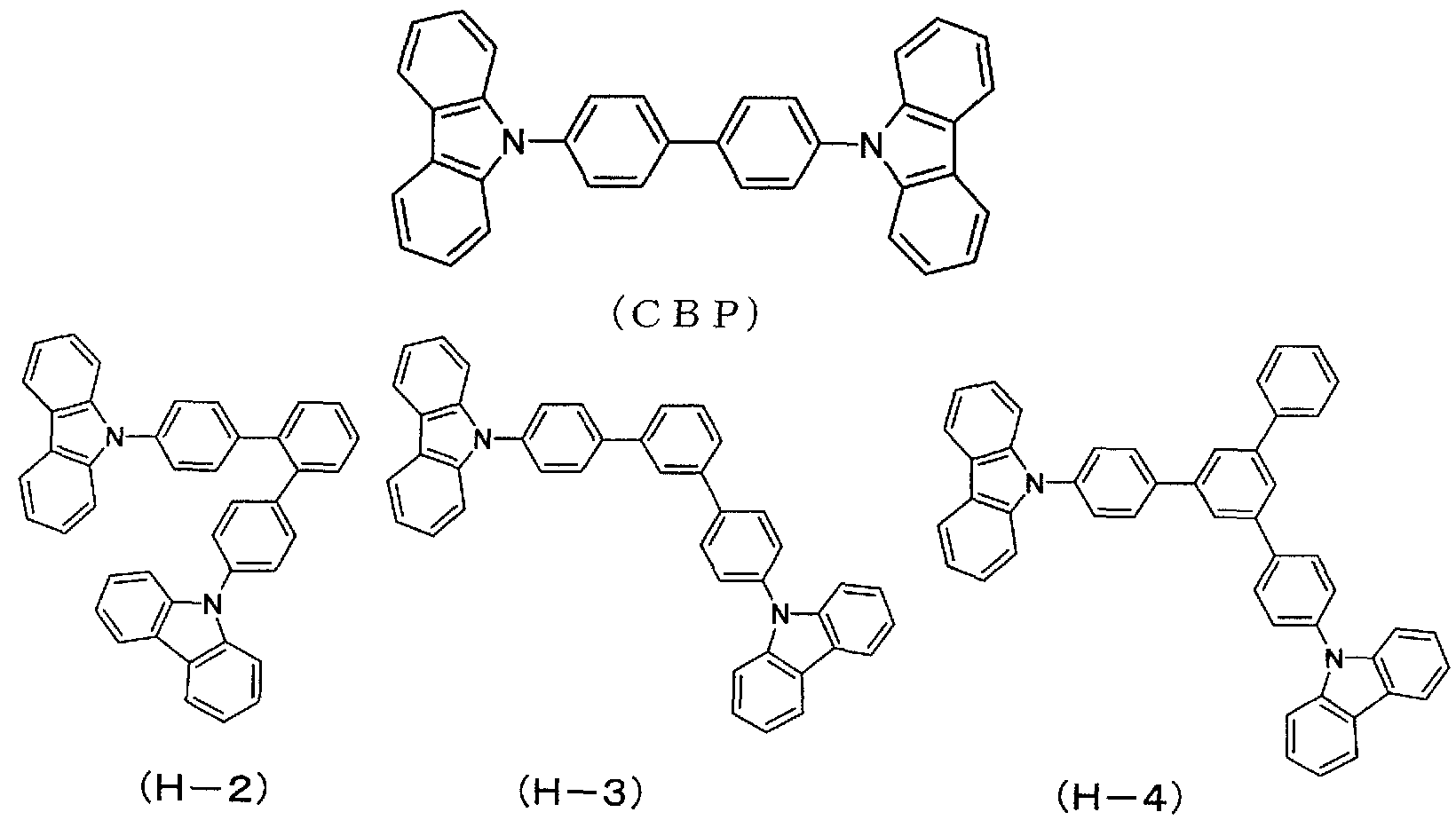
- 4,4-N, N-dicarbazole biphenyl is used as a host compound. This compound has a glass transition temperature of 110 ° C. or lower, and has a good symmetry.
- Patent Document 6 Patent Document 7, Patent Document 8, Patent Document 9, Patent Document 10, Patent Document 10). Etc.
- Patent Document 6 Patent Document 7
- Patent Document 8 Patent Document 9, Patent Document 10
- Etc. the heat resistance is improved in Patent Document 6
- most of the phenylene structure constituting the compound adopts a bonding mode of bonding at the para position, and the bond at the meta position is only the central benzene ring. So the problem of crystallization, which still has good symmetry, is avoided Did not.
- Patent Documents 7 and 8 disclose a host material in which a heterocyclic skeleton such as a triazine skeleton is further introduced in addition to a phenolic skeleton.
- Patent Documents 9 and 10 disclose, in addition to the phenylene structure that constitutes the compound, a structure in which a diarylaminophenol group and a aryl group are bonded to the benzene ring at the S meta position. This has improved the life and heat resistance, but was not practically sufficient.
- Patent Document 1 Japanese Patent Application Laid-Open No. 8-239655
- Patent Document 2 JP-A-7-138561
- Patent Document 3 JP-A-3-200289
- Patent Document 4 U.S. Pat.No. 6,097,147
- Patent Document 5 International Publication WO01Z41512
- Patent Document 6 JP-A-2003-31371
- Patent Document 7 JP-A-2002-193952
- Patent Document 8 EP1202608 specification
- Patent Document 9 JP-A-10-237438
- Patent Document 10 International Publication WO01Z72927
- Non-patent Reference 1 D.F.O'Brien and M.A.Balao et al 'Improved energy transfenn electrophosphorescent devices "Applied Physics letters Vol. 74 No.3, pp442 ⁇ 444, January 18, 1999
- Non-Patent Document 2 M.A.Baldo et al "Very high-efficiency green organic light-emitting devices based on electrophosphorescence Applied Physics letters Vol. 75 No. 1, pp4-6, July 5, 1999
- the present invention has been made to solve the above-described problems, and has high heat-resistance and high luminous efficiency. It is an object of the present invention to provide a material for an organic EL device having excellent durability and a long life, and an organic EL device using the same.
- an organic EL device having high efficiency, high heat resistance and long life can be obtained by using a conjugate having a large molecular weight and large steric hindrance represented by 1) as a host material.
- the present invention has been achieved.
- the present invention provides a compound represented by the following general formula (1), which is a material for an organic EL device.
- [Ar] is an aryl group having 6 to 24 nuclear carbon atoms which may have a substituent, a rubazolyl group which may have a substituent, a carbazolylphenyl group which may have a substituent. Is also the chosen group.
- R is a group represented by the following general formula (2) or (3).
- At least one of R and R is a group represented by the following general formula (2) or (3), and the rest is
- the following general formula (2) and the following general formula (3) are an aryl group having a nuclear carbon atom of 6 to 24 which may have a hydrogen atom or a substituent.
- R represents a hydrogen atom or a substituted or unsubstituted aryl group having 6 to 24 nuclear carbon atoms.
- the present invention provides an organic EL device in which one or more organic thin film layers having at least a light emitting layer are sandwiched between a cathode and an anode, wherein at least one of the organic thin film layers is
- An object of the present invention is to provide an organic EL device containing a material for an organic EL device. The invention's effect
- An organic EL device using the material for an organic EL device of the present invention has high luminous efficiency, excellent heat resistance, and long life.
- the organic EL device material of the present invention also has a compound power represented by the following general formula (1).
- Ar represents an aryl group having 6 to 24 nuclear carbon atoms (preferably 6 to 18 nuclear carbon atoms) which may have a substituent, or a carbazolyl group which may have a substituent. And a carbazolylphenyl group which may have a substituent.
- Examples of the aryl group having 6 to 24 carbon atoms which may have a substituent include phenyl, 1 naphthyl, 2 naphthyl, 1 anthryl, 2 anthryl, and 9 anthryl. , 1-phenanthryl group, 2-phenanthryl group, 3-phenanthryl group, 4 phenanthryl group, 9 phenanthryl group, 1 naphthatel group, 2 naphthatel group, 9 naphthatel group, 1-pyrreyl group, 2— Pyreyl group, 4-pyryl group, 2-biphenyl-yl group, 3-biphenyl-yl group, 4-biphenyl-yl group, 2,3-diphenyl-yl group, 2,4-diphenyl-yl group Phenyl, 2,5-diphenyl, 2,6-diphenyl, 3,4-diphenyl, 3,5-diphenyl, p Tarferu 4-yl, p Tarferu 3-yl, p
- Examples of the substituent for the aryl group, carbazolyl group, and carbazolylphenyl group include a halogen atom, a hydroxyl group, an amino group, a nitro group, a nitro group, a cyano group, an alkyl group, an alkyl group, a cycloalkyl group, an alkoxy group, Aryl group, heteroaryl group, aralkyl group, aryl group An alkoxy group, an alkoxycarbonyl group, etc., and more preferably a straight-chain, branched or cyclic alkyl group or alkoxy group having 1200 carbon atoms, an aryl group or a heteroaryl group having 120 carbon atoms is more preferable.
- alkyl group of 1 one 8 carbon atoms e.g., methyl group, Echiru group, i so - propyl, tert - butyl, n - Okuchiru group, n - decyl group, n - to Kisadeshiru group, cyclopropyl group , A cyclopentyl group, a cyclohexyl group and the like.
- R is a group represented by the following general formula (2) or (3).
- R and R are represented by the following general formula (2) or (3).
- R is a hydrogen atom or a C 6-24 carbon atom which may have a substituent.
- aryl group having 6 to 24 nuclear carbon atoms which may have a substituent for R include those described above.
- R, R and R each independently represent a hydrogen atom or It is a substitution group.
- substituents examples include the same as those described above for Ar, and preferable examples thereof are also the same.
- R or R, R and force be a group represented by the general formula (2).
- the material for an organic EL device of the present invention is preferably a host material contained in the light emitting layer of the organic EL device.
- organic EL device material represented by the general formula (1) according to the present invention are shown below, but are not limited to these exemplary compounds.
- the organic EL device of the present invention is an organic EL device in which one or more organic thin film layers having at least a light-emitting layer are sandwiched between a cathode and an anode. Of the organic EL element.
- a light emitting layer is provided between an anode and a cathode.
- the light-emitting layer contains a light-emitting material, and may also contain a hole-injection material or an electron-injection material for transporting holes injected with anodic force or electrons injected from the cathode to the light-emitting material.
- the light emitting material has extremely high fluorescence quantum efficiency, high hole transport ability and electron transport ability, and forms a uniform thin film.
- the multi-layer organic EL device has an anode Z a hole injection layer (hole transport layer) Z light emitting layer Z cathode, an anode Z light emitting layer Z an electron injection layer (electron transport layer) Z cathode, an anode Z a hole injection layer (positive Hole transport layer) / light-emitting layer Z electron injection layer (electron transport layer) Z cathode, anode Z hole injection layer (hole transport layer) Z light emitting layer Z hole blocking layer Z electron injection layer (electron transport layer) Z Those laminated in a multilayer structure such as a cathode are exemplified.
- the light emitting layer or the hole injection layer (hole transport layer) contains the material for an organic EL device of the present invention. More preferred.
- the compound represented by the general formula (1) used in the present invention has an excellent hole transporting property, can stably inject holes, has a high glass transition point (preferably 120 to 160 ° C), and has a light emitting material. Since non-radiative transitions caused by interactions that can interact with each other are avoided, the luminance, heat resistance, lifespan, and luminous efficiency of the organic EL element are improved by including it in at least one of the organic thin film layers of the organic EL element. .
- the light-emitting layer contains a host material and a phosphorescent light-emitting material, and the host material also has a compound power represented by the general formula (1) of the present invention. It is preferably a material.
- the phosphorescent light-emitting material is selected from the group consisting of Ir, Ru, Pd, Pt, Os, and Re, because the external quantum efficiency of the light-emitting device having a high phosphorescence quantum yield can be further improved.
- the metal complex contains at least one metal. The reason for this is that if the phosphorescent light emitting material is a metal complex of these metals, it can be represented by the general formula (1) as a host material. This is because, when a compound to be used is used, the triplet exciton force of the compound force can effectively transfer energy.
- the phosphorescent light-emitting materials include tris (2-phenylpyridine) iridium, tris (2-phenylpyridine) ruthenium, tris (2-phenylpyridine) palladium, and tris (2-phenylpyridine) palladium.
- (2-Phenylrubidine) platinum Tris (2-phenylpyridine) osmium, Tris (2-phenylpyridine) rhenium, Otataethylplatinum porphyrin, Octaphenylplatinum porphyrin, Otataethylpalladium porphyrin, Octaferubaladium porphyrin
- metal complexes such as bis (4,6-difluorophenylpyridine) picolinatotoridium.
- Metal complexes containing Ir for more efficient energy transfer and fluorescence emission for example, the following structure Is preferably tris (2-phenylpyridine) iridium represented by the formula:
- At least one of the ligands of the metal complex has a phenylubiridine skeleton, a biviridyl skeleton, or a phenanthone-containing phosphorus skeleton.
- the reason for this is that by having these electron-withdrawing skeletons in the molecule, the triplet force of the phorbazole derivative can effectively transfer energy.
- the amount of the phosphorescent light-emitting material is preferably 0.1 to 30 parts by weight with respect to 100 parts by weight of the compound of the general formula (1). In this case, it is more preferable that the amount be 1 to 15 parts by weight. The reason for this is that When the amount is 0.1 part by weight or more, the effect of addition is exhibited, and the triplet exciton force of the compound of the general formula (1) can also effectively transfer energy, so that the phosphorescent luminescent material is used. If the content is less than 30 parts by weight, it is easy to uniformly mix the phosphorescent light emitting material, and the emission luminance does not vary.
- the known hole injecting material contained in the hole injecting layer has a capability of transporting holes, and has a hole transporting property.
- Compounds having an injection effect, an excellent hole injection effect on the light emitting layer or the light emitting material, preventing excitons generated in the light emitting layer from moving to the electron injection layer, and having excellent thin film forming ability are preferable.
- a more effective hole injecting material is an aromatic tertiary amine derivative or a phthalocyanine derivative.
- the aromatic tertiary amine derivative include triphenylamine, tritolylamine, tolyldiphenylamine, N, ⁇ '-diphenyl-2-, ⁇ , N '-(3-methylphenyl) -1,1,1-biphenyl- 4, 4 'Jiamin, ⁇ , ⁇ , ⁇ ', N '— (4 Methylfeil) — 1, 1'—Pheru 4, 4' Jiamin, ⁇ , ⁇ , ⁇ ', ⁇ '— (4 Methylfue -Le) 1, 1'-bihue-ru 4, 4 'Jiamin, ⁇ , N'-dihue-ru ⁇ , N'-Dinaphthyl 1, 1'-bihue-ru 4, 4
- phthalocyanine (Pc) derivative examples include HPc, CuPc, CoPc, NiPc, ZnPc, PdPc, FePc, MnPc, ClAlPc, ClGa Pc ClInPc ClSnPc CI SiPc (HO) AlPc (HO) GaPc VOPc TiOPc Mo
- OPc GaPc a phthalocyanine derivative such as O—GaPc and a naphthalocyanine derivative, but are not limited thereto.
- the electron injection material contained in the above-mentioned known electron injection layer has the ability to transport electrons, has the effect of injecting electrons from the cathode, Compounds that have an excellent electron-injection effect on the light-emitting layer or the light-emitting material, prevent excitons generated in the light-emitting layer from moving to the hole-injection layer, and have excellent thin-film formation ability are preferred.
- more effective electron injection materials are metal complex conjugates or nitrogen-containing five-membered ring derivatives.
- Examples of the metal complex conjugate include 8-hydroxyquinolina tritium, bis (8-hydroxyquinolinato) zinc, bis (8-hydroxyquinolinato) copper, bis (8-hydroxyquinone) Nolinato) manganese, tris (8-hydroxyquinolinato) aluminum, tris (2-methyl-8-hydroxyquinolinato) aluminum, tris ( 8 -hydroxyquinolinato) gallium, bis
- the nitrogen-containing five-membered derivative is preferably an oxazole, thiazole, oxaziazole, thiaziazole or triazole derivative. More specifically, 2,5-bis (1-phenyl) -1,3,4-oxazole, dimethyl POPOP 2,5-bis (1-phenyl) -1,3,4-thiazole, 2 , 5 bis (1 phenol) — 1,3,4 oxaziazole, 2— (4 tert-butyl) (Tilphenyl) — 5— (4'-biphenyl) 1,3,4-oxadiazole, 2,5-bis (1-naphthyl) —1,3,4-oxadiazole, 1,4— Bis [2— (5-phenoxadiazolyl)] benzene, 1,4 Bis [2— (5-fuoxadiazolyl) 4 tertbutylbenzene, 2— (4'-tert Butylphenyl) -5- (4'-
- an inorganic compound layer may be provided between the light emitting layer and the electrode to improve charge injection.
- examples of such an inorganic compound layer include alkali metal compounds (such as fluorides and oxides) and alkaline earth metal compounds. Specifically, LiF, Li0, RaO, SrO, BaF , SrF and the like.
- hole blocking layer having a thickness of 5 nm to 5 m between the light emitting layer and the cathode.
- hole blocking materials include 2,9-dimethyl-4,7-diphenyl-1,10 phenanthroline and 2,9-diethyl-4,7-diphenyl-1,10 phenanthroline. It is preferable to further contain an alkali metal, for example, Li or Cs.
- the driving voltage of the organic EL element can be significantly reduced, and the life can be extended. it can.
- the content is preferably 0.01 to 30% by weight, when the total amount of the hole blocking layer is 100% by weight, and 0.05 to 20% by weight. Is more preferable, and 0.1 to 15 parts by weight is particularly preferable. The reason is that if the content of strong alkali metal is 0.01% by weight or more, the effect of addition is surely exhibited, and if the content is 30% by weight or less, the dispersibility of the alkali metal becomes uneven. There is no case where the emission luminance varies!
- the conductive material used for the anode of the organic EL device of the present invention is a material larger than 4 eV.
- a material larger than 4 eV are suitable for use with carbon, aluminum, vanadium, iron, cobalt, nickel, tungsten, silver, gold, platinum, palladium, and their alloys, and tin oxide used for ITO and NES A substrates.
- metal oxides such as indium oxide, and organic conductive resins such as polythiophene and polypyrrole.
- the conductive material used for the cathode those having a work function of less than 4 eV are suitable, and magnesium, calcium, tin, lead, titanium, yttrium, lithium, ruthenium, manganese, aluminum, etc.
- the force used by the alloy is not limited to these.
- Typical examples of the alloy include magnesium zirconium, magnesium Z indium, lithium Z aluminum and the like, but are not limited thereto.
- the ratio of the alloy is controlled by the temperature, atmosphere, degree of vacuum, and the like of the evaporation source, and is selected to be an appropriate ratio.
- the anode and the cathode may be formed of two or more layers if necessary.
- a reducing dopant is added to an interface region between the cathode and the organic thin film layer.
- Examples of the reducing dopant include alkali metals, alkali metal complexes, alkali metal compounds, alkaline earth metals, alkaline earth metal complexes, alkaline earth metal compounds, rare earth metals, rare earth metal complexes, and rare earth metal compounds. There is at least one selected one.
- alkali metal examples include Na (work function: 2.36 eV), K (work function: 2.28 eV), Rb (work function: 2.16 eV), and Cs (work function: 1.95 eV). And those having a work function of 2.9 eV or less are particularly preferable. Of these, K, Rb and Cs are preferred, Rb and Cs are more preferred, and Cs is most preferred.
- alkaline earth metal examples include Ca (work function: 2.9 eV), Sr (work function: 2.0-2.5 eV), Ba (work function: 2.52 eV), and the like. Particularly preferred is 9 eV or less.
- rare earth metal examples include Sc, Y, Ce, Tb, and Yb, and those having a work function of 2.9 eV or less are particularly preferable.
- alkali metal compound examples include alkali oxides such as Li0, Cs0, and KO; LiF;
- alkali halides such as NaF, CsF, and KF.
- Potassium chloride or alkali fluoride is preferred.
- alkaline earth metal compound examples include BaO, SrO, CaO and a mixture thereof, BaSr ⁇ (0 ⁇ ⁇ 1), BaCaO (0 ⁇ x ⁇ 1), and the like.BaO, SrO, CaO x l- ⁇ x 1- ⁇
- rare earth metal compound YbF, ScF, ScO, YO, CeO, GdF, T
- 33323232bF and the like and YbF, ScF and TbF are preferable.
- the alkali metal complex, alkaline earth metal complex, and rare earth metal complex are not particularly limited as long as they contain at least one of an alkali metal ion, an alkaline earth metal ion, and a rare earth metal ion as metal ions, respectively. There is no limitation.
- ligands include quinolinol, benzoquinolinol, ataridinol, phenanthridinol, hydroxyphenyloxazole, hydroxyphenylthiazole, hydroxydiaryloxadiazole, hydroxydiarylthiadiazole, hydroxy Phenylviridine, hydroxyphenylbenzoimidazole, hydroxybenzotriazole, hydroxyfluborane, bipyridyl, phenanthine phosphorus, phthalocyanine, porphyrin, cyclopentadiene, 13 diketones, azomethines, and derivatives thereof Etc. are preferred, but not limited to these
- the reducing dopant is formed in a layer shape or an island shape in the interface region.
- a forming method a method in which a reducing dopant is deposited by a resistance heating deposition method, and at the same time, a luminescent material forming an interface region and an organic substance which is an electron injection material are simultaneously deposited, and the reducing dopant is dispersed in the organic substance is preferable.
- the reducing dopant is formed in a layered form, after forming the light emitting material or the electron injecting material, which is an organic layer at the interface, in a layered form, the reducing dopant is deposited alone by a resistance heating evaporation method, and preferably, the thickness of the layer is reduced to 0. . Formed with 1-15nm.
- the reducing dopant When the reducing dopant is formed in an island shape, the light emitting material or the electron which is the organic layer at the interface is used. After the implanted material is formed in the shape of an island, the reducing dopant is independently deposited by a resistance heating vapor deposition method, and is preferably formed to have an island thickness of 0.05 to 1 nm.
- the organic EL device of the present invention it is desirable that at least one surface is sufficiently transparent in the emission wavelength region of the device in order to emit light efficiently. It is also desirable that the substrate is transparent.
- the transparent electrode is set using the above-mentioned conductive material so as to secure a predetermined translucency by a method such as vapor deposition or sputtering. It is desirable that the electrode on the light emitting surface has a light transmittance of 10% or more.
- the substrate is not limited as long as it has mechanical and thermal strength and transparency, but includes a glass substrate and a transparent resin film.
- Transparent resin films include polyethylene, ethylene-vinyl acetate copolymer, ethylene-vinyl alcohol copolymer, polypropylene, polystyrene, polymethyl methacrylate, polyvinyl chloride, polyvinyl alcohol, polybutyl butyral, and nylon.
- examples include xafluoropropylene copolymer, polychlorinated trifluoroethylene, polyvinylidene fluoride, polyester, polycarbonate, polyurethane, polyimide, polyetherimide, polyimide, and polypropylene. It is.
- a protective layer may be provided on the surface of the device, or the entire device may be protected with silicon oil, resin, or the like in order to improve stability against temperature, humidity, atmosphere, and the like.
- a shift method such as a dry film forming method such as vacuum evaporation, sputtering, plasma, or ion plating, or a wet film forming method such as spin coating, divebing, or flow coating can be applied. it can.
- the film thickness is not particularly limited, but needs to be set to an appropriate film thickness. If the film thickness is too large, a large applied voltage is required to obtain a constant light output, resulting in poor efficiency.
- a normal film thickness is preferably in the range of 5 nm to 10 m.
- a force in the range of 10 nm to 0.2 m is more preferable.
- the material for forming each layer is ethanol
- the thin film is formed by dissolving or dispersing in an appropriate solvent such as furan or dioxane, and any solvent may be used.
- a suitable resin additive may be used to improve film forming properties, prevent pinholes in the film, and the like.
- resins that can be used include insulating resins such as polystyrene, polycarbonate, polyarylate, polyester, polyamide, polyurethane, polysulfone, polymethyl methacrylate, polymethyl acrylate, and cellulose, and copolymers thereof.
- Examples thereof include photoconductive resins such as coalesce, poly-N-vinylcarbazole and polysilane, and conductive resins such as polythiophene and polypyrrole.
- Examples of the additives include an antioxidant, an ultraviolet absorber, and a plasticizer.
- the reaction solution was cooled to room temperature, methylene chloride and water were added, and after separating into two layers, the organic layer was washed with 5% hydrochloric acid and water, and dried over anhydrous sodium sulfate. After evaporating the organic solvent under reduced pressure, 500 ml of ethanol was removed, and the precipitated crystals were filtered and washed with ethanol and normal hexane in that order to obtain 178 g of a bromophenolcarbazole derivative.
- 160 g is dissolved in 1,000 ml of toluene (dehydrated solvent manufactured by Wako Pure Chemical Industries) and 1000 ml of ether (dehydrated solvent manufactured by Wako Pure Chemical Industries), and n-butyl lithium hexane solution (Wako Pure Chemical Industries, Ltd.) at -40 ° C under an argon atmosphere. (1.6M) was stirred at -40 ° C for 1 hour at 0 ° C. Next, the reaction solution was cooled to -70 ° C, and a solution obtained by diluting 340 ml of triisopropyl borate (manufactured by Tokyo Chemical Industry) with 500 ml of ether (dehydrated solvent manufactured by Wako Pure Chemical Industries) was added dropwise. After stirring for an hour, the mixture was heated to room temperature and stirred for 6 hours.
- reaction solution was left at room temperature, filtered, and the crystals were washed with DME, water and methanol in that order, and dried to obtain 3,4-bis (4- (carbazolyl-9-yl) phenyl) -1. — 3.4 g of bromobenzene (intermediate B).
- reaction solution was extracted with methylene chloride, added with lg of sodium bisulfite, separated, dried over anhydrous sodium sulfate, and the solvent was distilled off under reduced pressure. Mouth mode benzene was obtained.
- the glass substrate with the ITO transparent electrode having a thickness of 25 mm ⁇ 75 mm ⁇ 0.7 mm was subjected to ultrasonic cleaning for 5 minutes in isopropyl alcohol, and then to UV ozone cleaning for 30 minutes.
- the washed glass substrate with a transparent electrode is mounted on a substrate holder of a vacuum evaporation apparatus.
- the copper phthalocyanine having a film thickness of 10 nm is coated on the surface on the side where the transparent electrode is formed so as to cover the transparent electrode.
- a film hereinafter abbreviated as “CuPc film” was formed. This CuPc film functions as a hole injection layer.
- ⁇ -NPD film 4,4,1-bis [N— (1naphthyl) Nphenylamino] biphenyl film (hereinafter abbreviated as “ ⁇ -NPD film”) with a thickness of 30 nm is formed on this film. Is formed.
- This ⁇ NPD film functions as a hole transport layer.
- the compound (A-1) having a thickness of 30 nm was deposited as a host material on the NPD film to form a light emitting layer.
- tris (2-phenolylidine) Ir hereinafter abbreviated as “Ir (ppy)” was added as a phosphorescent Ir metal complex dopant.
- the concentration of Ir (ppy) in the light emitting layer was 5% by weight. This film functions as a light emitting layer.
- BAlq film (1, 1-bisphenol) -4-olato) bis (2-methyl-8-quinolinolate) aluminum
- BA1 q film functions as a hole barrier layer.
- Alq film an aluminum complex of the following 8-hydroxyquinoline (hereinafter abbreviated as “Alq film”) having a thickness of 40 nm was formed on the film.
- Alq film functions as an electron injection layer.
- an alkali metal halide, LiF was deposited to a thickness of 0.2 nm, and then aluminum was deposited to a thickness of 150 nm.
- This AlZLiF works as a cathode.
- an organic EL device was produced.
- This device was subjected to a conduction test. As a result, at a voltage of 5.7 V and a current density of 0.26 mA / cm 2 , green luminescence with an emission luminance of 99 cdZm 2 was obtained, and the chromaticity coordinates were (0.32, 0.61). ), The luminous efficiency was 38.7 cdZA. Further, the device is driven initial luminance 5000CdZm 2 Nitejo current, the time to half to luminance 2500CdZm 2 was 622 hours.
- An organic EL device was prepared in the same manner as in Example 1 except that the compounds shown in Table 1 were used instead of the compound (A-1) as the host material of the light emitting layer.
- the voltage, current density, luminance, luminous efficiency, chromaticity, luminance half-life, and heat-resistant current emission time were measured and shown in Table 1.
- An organic EL device was prepared in the same manner as in Example 1 except that the following compound shown in Table 1 was used instead of the compound (A-1) as the host material of the light emitting layer. Similarly, the voltage, current density, luminance, luminous efficiency, chromaticity, luminance half-life, and heat-resistant current-emission time were measured and shown in Table 1.
- the organic EL device using the compound of the present invention can emit green light with high efficiency, long life and high heat resistance.
- Example 1 the above compound (B-10) was used in place of the compound (A-1) as the host material of the light emitting layer, and the following bis (2) was used in place of Ir (ppy) as the phosphorescent metal complex dopant.
- An organic EL device was fabricated by the same method except that benzochelpyridine) acetylacetonertoiridium (Ir (btp) (acac)) was used.
- This device was subjected to a conduction test. As a result, at a voltage of 7.4 V and a current density of 2.3 mA / cm 2 , red light emission having a luminance of 100 cdZm 2 was obtained, and the chromaticity coordinates were (0.66, 0.32). ), The luminous efficiency was 4.3 cdZA. Further, the element constant current was driven at an initial luminance 500CdZm 2, the time to half to luminance 250CdZm 2 was 1742 hours. In addition, as a heat resistance test, the device was energized under 105 ° C environmental conditions and the heat-resistant energized emission time was measured. It was confirmed that red light emission with sufficient emission luminance was obtained even after 500 hours had passed after the energization. Table 2 shows the results.
- An organic EL device was prepared in the same manner as in Example 5 except that the compound (A-19) was used in place of the compound (B-10) as the host material of the light emitting layer. Measure voltage, current density, luminance, luminous efficiency, chromaticity, luminance half-life, heat-resistant energizing luminescence time
- An organic EL device was prepared in the same manner as in Example 5 except that the above compound (CBP) was used instead of the compound (B-10) as the host material of the light emitting layer. Measures current density, luminance, luminous efficiency, chromaticity, luminance half-life, heat-resistant current-emitting time
- Example 5 a compound (H-3) or (H-4) described in Table 2 was used in place of the compound (B-10) as the host material for the light emitting layer, in the same manner.
- Organic EL device It was fabricated and measured for voltage, current density, luminance, luminous efficiency, chromaticity, luminance half-life, and heat-resistant current-emitting time in the same manner as in Example 5. The results are shown in Table 2.
- the organic EL device using the compound of the present invention can emit red light with high efficiency, long life and high heat resistance.
- the use of the compound for an organic EL device of the present invention which is a compound represented by the general formula (1), has high luminous efficiency, excellent heat resistance, and long life. Is obtained. For this reason, the organic EL device of the present invention is extremely useful as a light source for various electronic devices.
Landscapes
- Chemical & Material Sciences (AREA)
- Organic Chemistry (AREA)
- Engineering & Computer Science (AREA)
- Materials Engineering (AREA)
- Physics & Mathematics (AREA)
- Spectroscopy & Molecular Physics (AREA)
- Electroluminescent Light Sources (AREA)
Abstract
Description




Claims

Priority Applications (3)
| Application Number | Priority Date | Filing Date | Title |
|---|---|---|---|
| JP2006511019A JPWO2005089027A1 (ja) | 2004-03-17 | 2005-03-14 | 有機エレクトロルミネッセンス素子用材料及びそれを用いた有機エレクトロルミネッセンス素子 |
| US10/592,949 US20070190356A1 (en) | 2004-03-17 | 2005-03-14 | Material for organic electroluminescent element and organic electroluminescent element employing the same |
| EP05720688A EP1727397A4 (en) | 2004-03-17 | 2005-03-14 | MATERIAL FOR ORGANIC ELECTROLUMINESCENE ELEMENT AND ITS USE IN ORGANIC ELECTROLUMINESCENE ELEMENT |
Applications Claiming Priority (2)
| Application Number | Priority Date | Filing Date | Title |
|---|---|---|---|
| JP2004076047 | 2004-03-17 | ||
| JP2004-076047 | 2004-03-17 |
Publications (1)
| Publication Number | Publication Date |
|---|---|
| WO2005089027A1 true WO2005089027A1 (ja) | 2005-09-22 |
Family
ID=34976002
Family Applications (1)
| Application Number | Title | Priority Date | Filing Date |
|---|---|---|---|
| PCT/JP2005/004417 Ceased WO2005089027A1 (ja) | 2004-03-17 | 2005-03-14 | 有機エレクトロルミネッセンス素子用材料及びそれを用いた有機エレクトロルミネッセンス素子 |
Country Status (7)
| Country | Link |
|---|---|
| US (1) | US20070190356A1 (ja) |
| EP (1) | EP1727397A4 (ja) |
| JP (1) | JPWO2005089027A1 (ja) |
| KR (1) | KR20060134987A (ja) |
| CN (1) | CN1934909A (ja) |
| TW (1) | TW200540251A (ja) |
| WO (1) | WO2005089027A1 (ja) |
Cited By (6)
| Publication number | Priority date | Publication date | Assignee | Title |
|---|---|---|---|---|
| JP2007180277A (ja) * | 2005-12-28 | 2007-07-12 | Konica Minolta Holdings Inc | 有機エレクトロルミネッセンス素子、表示装置及び照明装置 |
| WO2009082583A3 (en) * | 2007-12-18 | 2009-09-03 | Motorola, Inc. | An organic composition and method of producing an electronic article comprising the organic composition |
| KR101177959B1 (ko) | 2005-04-01 | 2012-08-28 | 소니 주식회사 | 셀룰라 통신 시스템에서의 흐름 제어 |
| JP2012226891A (ja) * | 2011-04-18 | 2012-11-15 | Seiko Epson Corp | 有機el装置およびその製造方法、電子機器 |
| WO2014104235A1 (ja) * | 2012-12-28 | 2014-07-03 | 東ソー株式会社 | 1,2,4-トリス置換ベンゼン化合物とその製造方法、および有機電界発光素子 |
| JP2023501966A (ja) * | 2019-10-31 | 2023-01-20 | ソールブレイン・カンパニー・リミテッド | 有機化合物、それを含む有機発光ダイオード、及び該有機発光ダイオードを含む表示装置 |
Families Citing this family (8)
| Publication number | Priority date | Publication date | Assignee | Title |
|---|---|---|---|---|
| PL1986473T3 (pl) * | 2007-04-03 | 2017-07-31 | Tsinghua University | Organiczne urządzenie elektroluminescencyjne |
| KR101282178B1 (ko) * | 2010-01-18 | 2013-07-04 | 덕산하이메탈(주) | 다양한 치환기를 갖는 방향족 아민 화합물 및 이를 이용한 유기전자소자, 그 단말 |
| KR101423173B1 (ko) | 2010-11-04 | 2014-07-25 | 제일모직 주식회사 | 유기광전소자용 화합물 및 이를 포함하는 유기광전소자 |
| KR102050029B1 (ko) * | 2011-08-26 | 2019-11-29 | 삼성디스플레이 주식회사 | 도너 기판, 도너 기판의 제조 방법, 유기 발광 표시 장치 및 유기 발광 표시 장치의 제조 방법 |
| KR102923733B1 (ko) * | 2018-12-28 | 2026-02-04 | 삼성전자주식회사 | 헤테로시클릭 화합물, 이를 포함하는 조성물 및 이를 포함하는 유기 발광 소자 |
| EP4174054A1 (en) | 2018-12-28 | 2023-05-03 | Samsung Electronics Co., Ltd. | Heterocyclic compound, composition including the same, and organic light-emitting device including the heterocyclic compound |
| KR102753926B1 (ko) * | 2019-03-11 | 2025-01-15 | 삼성디스플레이 주식회사 | 헤테로시클릭 화합물 및 이를 포함한 유기 발광 소자 |
| CN112635529B (zh) * | 2020-12-18 | 2024-08-13 | 北京维信诺科技有限公司 | 显示面板及其制备方法、显示装置 |
Citations (4)
| Publication number | Priority date | Publication date | Assignee | Title |
|---|---|---|---|---|
| JPH08259940A (ja) * | 1995-03-08 | 1996-10-08 | Eastman Kodak Co | 高い熱安定性を有する有機エレクトロルミネセンス装置 |
| JP2001313178A (ja) * | 2000-04-28 | 2001-11-09 | Pioneer Electronic Corp | 有機エレクトロルミネッセンス素子 |
| JP2003031371A (ja) * | 2001-07-17 | 2003-01-31 | Mitsubishi Chemicals Corp | 有機電界発光素子及び青色発光素子 |
| JP2003048868A (ja) * | 2001-08-01 | 2003-02-21 | Mitsui Chemicals Inc | アミン化合物、その製造方法および該アミン化合物を含有する有機電界発光素子 |
Family Cites Families (7)
| Publication number | Priority date | Publication date | Assignee | Title |
|---|---|---|---|---|
| JP3266573B2 (ja) * | 1998-04-08 | 2002-03-18 | 出光興産株式会社 | 有機エレクトロルミネッセンス素子 |
| US6097147A (en) * | 1998-09-14 | 2000-08-01 | The Trustees Of Princeton University | Structure for high efficiency electroluminescent device |
| US6661023B2 (en) * | 2002-02-28 | 2003-12-09 | Eastman Kodak Company | Organic element for electroluminescent devices |
| JP2003317946A (ja) * | 2002-04-23 | 2003-11-07 | Konica Minolta Holdings Inc | 有機el素子及び有機el素子の製造方法 |
| JP4103491B2 (ja) * | 2002-08-07 | 2008-06-18 | コニカミノルタホールディングス株式会社 | 有機エレクトロルミネッセンス素子及び表示装置 |
| EP2248870B1 (en) * | 2002-11-26 | 2018-12-26 | Konica Minolta Holdings, Inc. | Organic electroluminscent element and display and illuminator |
| KR20060127059A (ko) * | 2004-01-21 | 2006-12-11 | 이데미쓰 고산 가부시키가이샤 | 유기 전기 발광 소자용 호스트 재료 및 유기 전기 발광소자 |
-
2005
- 2005-03-14 US US10/592,949 patent/US20070190356A1/en not_active Abandoned
- 2005-03-14 WO PCT/JP2005/004417 patent/WO2005089027A1/ja not_active Ceased
- 2005-03-14 CN CNA2005800087697A patent/CN1934909A/zh active Pending
- 2005-03-14 JP JP2006511019A patent/JPWO2005089027A1/ja active Pending
- 2005-03-14 KR KR1020067019098A patent/KR20060134987A/ko not_active Ceased
- 2005-03-14 EP EP05720688A patent/EP1727397A4/en not_active Withdrawn
- 2005-03-16 TW TW094108076A patent/TW200540251A/zh unknown
Patent Citations (4)
| Publication number | Priority date | Publication date | Assignee | Title |
|---|---|---|---|---|
| JPH08259940A (ja) * | 1995-03-08 | 1996-10-08 | Eastman Kodak Co | 高い熱安定性を有する有機エレクトロルミネセンス装置 |
| JP2001313178A (ja) * | 2000-04-28 | 2001-11-09 | Pioneer Electronic Corp | 有機エレクトロルミネッセンス素子 |
| JP2003031371A (ja) * | 2001-07-17 | 2003-01-31 | Mitsubishi Chemicals Corp | 有機電界発光素子及び青色発光素子 |
| JP2003048868A (ja) * | 2001-08-01 | 2003-02-21 | Mitsui Chemicals Inc | アミン化合物、その製造方法および該アミン化合物を含有する有機電界発光素子 |
Non-Patent Citations (1)
| Title |
|---|
| See also references of EP1727397A4 * |
Cited By (10)
| Publication number | Priority date | Publication date | Assignee | Title |
|---|---|---|---|---|
| KR101177959B1 (ko) | 2005-04-01 | 2012-08-28 | 소니 주식회사 | 셀룰라 통신 시스템에서의 흐름 제어 |
| JP2007180277A (ja) * | 2005-12-28 | 2007-07-12 | Konica Minolta Holdings Inc | 有機エレクトロルミネッセンス素子、表示装置及び照明装置 |
| WO2009082583A3 (en) * | 2007-12-18 | 2009-09-03 | Motorola, Inc. | An organic composition and method of producing an electronic article comprising the organic composition |
| JP2012226891A (ja) * | 2011-04-18 | 2012-11-15 | Seiko Epson Corp | 有機el装置およびその製造方法、電子機器 |
| US8846426B2 (en) | 2011-04-18 | 2014-09-30 | Seiko Epson Corporation | Organic EL device and manufacturing method thereof, and electronic apparatus |
| WO2014104235A1 (ja) * | 2012-12-28 | 2014-07-03 | 東ソー株式会社 | 1,2,4-トリス置換ベンゼン化合物とその製造方法、および有機電界発光素子 |
| JP2014141467A (ja) * | 2012-12-28 | 2014-08-07 | Tosoh Corp | 1,2,4−トリス置換ベンゼン化合物、その製造方法、および有機電界発光素子 |
| JP2023501966A (ja) * | 2019-10-31 | 2023-01-20 | ソールブレイン・カンパニー・リミテッド | 有機化合物、それを含む有機発光ダイオード、及び該有機発光ダイオードを含む表示装置 |
| JP7502431B2 (ja) | 2019-10-31 | 2024-06-18 | ソールブレイン・カンパニー・リミテッド | 有機化合物、それを含む有機発光ダイオード、及び該有機発光ダイオードを含む表示装置 |
| US12471490B2 (en) | 2019-10-31 | 2025-11-11 | Soulbrain Co., Ltd | Organic compound, organic light-emitting diode including organic compound, and display device including organic light-emitting diode |
Also Published As
| Publication number | Publication date |
|---|---|
| KR20060134987A (ko) | 2006-12-28 |
| EP1727397A1 (en) | 2006-11-29 |
| US20070190356A1 (en) | 2007-08-16 |
| CN1934909A (zh) | 2007-03-21 |
| JPWO2005089027A1 (ja) | 2008-01-31 |
| TW200540251A (en) | 2005-12-16 |
| EP1727397A4 (en) | 2008-07-02 |
Similar Documents
| Publication | Publication Date | Title |
|---|---|---|
| JP4060802B2 (ja) | 有機エレクトロルミネッセンス素子用材料及びそれを用いた有機エレクトロルミネッセンス素子 | |
| TWI429650B (zh) | Organic electroluminescent elements | |
| JP4464070B2 (ja) | アリールアミン化合物及びそれを用いた有機エレクトロルミネッセンス素子 | |
| CN101952389B (zh) | 发光元件材料及发光元件 | |
| KR101663527B1 (ko) | 신규한 유기발광화합물 및 이를 포함하는 유기전계발광소자 | |
| TWI466980B (zh) | Organic electroluminescent elements | |
| KR101861263B1 (ko) | 안트라센 유도체 및 이를 포함하는 유기전계발광소자. | |
| JP4002040B2 (ja) | 有機エレクトロルミネッセンス素子 | |
| JPWO2003080761A1 (ja) | 有機エレクトロルミネッセンス素子用材料及びそれを用いた有機エレクトロルミネッセンス素子 | |
| WO2007004364A1 (ja) | ピレン誘導体及びそれらを用いた有機エレクトロルミネッセンス素子 | |
| WO2002020460A1 (en) | Novel arylamine compounds and organic electroluminescent devices | |
| JP2008303152A (ja) | 新規銅錯体およびそれを用いた有機エレクトロルミネッセンス素子 | |
| WO2002020459A1 (en) | Novel styryl compounds and organic electroluminescent devices | |
| KR20130110347A (ko) | 인데노페난트렌 유도체 및 이를 포함하는 유기전계발광소자 | |
| JP2007049055A (ja) | 有機エレクトロルミネッセンス素子用材料および有機エレクトロルミネッセンス素子 | |
| CN108779080A (zh) | 新型化合物及包含它的有机发光元件 | |
| JP2008179697A (ja) | 有機エレクトロルミネッセンス素子用材料 | |
| JP2005082702A (ja) | 有機エレクトロルミネッセンス用素子材料およびそれを用いた有機エレクトロルミネッセンス素子 | |
| WO2005089027A1 (ja) | 有機エレクトロルミネッセンス素子用材料及びそれを用いた有機エレクトロルミネッセンス素子 | |
| JP2000290645A (ja) | 有機エレクトロルミネッセンス素子用材料およびそれを使用した有機エレクトロルミネッセンス素子 | |
| JP4525119B2 (ja) | 有機エレクトロルミネッセンス素子用材料およびそれを用いた有機エレクトロルミネッセンス素子 | |
| WO2009104733A1 (ja) | 有機エレクトロルミネッセンス素子用材料ならびに有機エレクトロルミネッセンス素子 | |
| JP2009197144A (ja) | 有機エレクトロルミネッセンス素子用材料ならびに有機エレクトロルミネッセンス素子 | |
| WO2012005724A1 (en) | Host material for organic light emitting devices | |
| JP2005113072A (ja) | 有機エレクトロルミネッセンス素子用材料およびそれを用いた有機エレクトロルミネッセンス素子 |
Legal Events
| Date | Code | Title | Description |
|---|---|---|---|
| AK | Designated states |
Kind code of ref document: A1 Designated state(s): AE AG AL AM AT AU AZ BA BB BG BR BW BY BZ CA CH CN CO CR CU CZ DE DK DM DZ EC EE EG ES FI GB GD GE GH GM HR HU ID IL IN IS JP KE KG KP KR KZ LC LK LR LS LT LU LV MA MD MG MK MN MW MX MZ NA NI NO NZ OM PG PH PL PT RO RU SC SD SE SG SK SL SM SY TJ TM TN TR TT TZ UA UG US UZ VC VN YU ZA ZM ZW |
|
| AL | Designated countries for regional patents |
Kind code of ref document: A1 Designated state(s): BW GH GM KE LS MW MZ NA SD SL SZ TZ UG ZM ZW AM AZ BY KG KZ MD RU TJ TM AT BE BG CH CY CZ DE DK EE ES FI FR GB GR HU IE IS IT LT LU MC NL PL PT RO SE SI SK TR BF BJ CF CG CI CM GA GN GQ GW ML MR NE SN TD TG |
|
| 121 | Ep: the epo has been informed by wipo that ep was designated in this application | ||
| WWE | Wipo information: entry into national phase |
Ref document number: 2006511019 Country of ref document: JP |
|
| WWE | Wipo information: entry into national phase |
Ref document number: 2005720688 Country of ref document: EP |
|
| WWE | Wipo information: entry into national phase |
Ref document number: 10592949 Country of ref document: US Ref document number: 2007190356 Country of ref document: US Ref document number: 1020067019098 Country of ref document: KR |
|
| WWE | Wipo information: entry into national phase |
Ref document number: 200580008769.7 Country of ref document: CN |
|
| NENP | Non-entry into the national phase |
Ref country code: DE |
|
| WWW | Wipo information: withdrawn in national office |
Ref document number: DE |
|
| WWE | Wipo information: entry into national phase |
Ref document number: 3831/CHENP/2006 Country of ref document: IN |
|
| WWP | Wipo information: published in national office |
Ref document number: 2005720688 Country of ref document: EP |
|
| WWP | Wipo information: published in national office |
Ref document number: 1020067019098 Country of ref document: KR |
|
| WWP | Wipo information: published in national office |
Ref document number: 10592949 Country of ref document: US |