WO2006001882A2 - Lead-free and cadmium-free conductive copper thick film pastes - Google Patents
Lead-free and cadmium-free conductive copper thick film pastes Download PDFInfo
- Publication number
- WO2006001882A2 WO2006001882A2 PCT/US2005/012743 US2005012743W WO2006001882A2 WO 2006001882 A2 WO2006001882 A2 WO 2006001882A2 US 2005012743 W US2005012743 W US 2005012743W WO 2006001882 A2 WO2006001882 A2 WO 2006001882A2
- Authority
- WO
- WIPO (PCT)
- Prior art keywords
- thick film
- glass
- mole
- glass composition
- film paste
- Prior art date
- Legal status (The legal status is an assumption and is not a legal conclusion. Google has not performed a legal analysis and makes no representation as to the accuracy of the status listed.)
- Ceased
Links
Classifications
-
- C—CHEMISTRY; METALLURGY
- C03—GLASS; MINERAL OR SLAG WOOL
- C03C—CHEMICAL COMPOSITION OF GLASSES, GLAZES OR VITREOUS ENAMELS; SURFACE TREATMENT OF GLASS; SURFACE TREATMENT OF FIBRES OR FILAMENTS MADE FROM GLASS, MINERALS OR SLAGS; JOINING GLASS TO GLASS OR OTHER MATERIALS
- C03C8/00—Enamels; Glazes; Fusion seal compositions being frit compositions having non-frit additions
- C03C8/02—Frit compositions, i.e. in a powdered or comminuted form
-
- C—CHEMISTRY; METALLURGY
- C03—GLASS; MINERAL OR SLAG WOOL
- C03C—CHEMICAL COMPOSITION OF GLASSES, GLAZES OR VITREOUS ENAMELS; SURFACE TREATMENT OF GLASS; SURFACE TREATMENT OF FIBRES OR FILAMENTS MADE FROM GLASS, MINERALS OR SLAGS; JOINING GLASS TO GLASS OR OTHER MATERIALS
- C03C3/00—Glass compositions
- C03C3/04—Glass compositions containing silica
- C03C3/062—Glass compositions containing silica with less than 40% silica by weight
- C03C3/064—Glass compositions containing silica with less than 40% silica by weight containing boron
-
- C—CHEMISTRY; METALLURGY
- C03—GLASS; MINERAL OR SLAG WOOL
- C03C—CHEMICAL COMPOSITION OF GLASSES, GLAZES OR VITREOUS ENAMELS; SURFACE TREATMENT OF GLASS; SURFACE TREATMENT OF FIBRES OR FILAMENTS MADE FROM GLASS, MINERALS OR SLAGS; JOINING GLASS TO GLASS OR OTHER MATERIALS
- C03C3/00—Glass compositions
- C03C3/04—Glass compositions containing silica
- C03C3/062—Glass compositions containing silica with less than 40% silica by weight
- C03C3/064—Glass compositions containing silica with less than 40% silica by weight containing boron
- C03C3/066—Glass compositions containing silica with less than 40% silica by weight containing boron containing zinc
-
- C—CHEMISTRY; METALLURGY
- C03—GLASS; MINERAL OR SLAG WOOL
- C03C—CHEMICAL COMPOSITION OF GLASSES, GLAZES OR VITREOUS ENAMELS; SURFACE TREATMENT OF GLASS; SURFACE TREATMENT OF FIBRES OR FILAMENTS MADE FROM GLASS, MINERALS OR SLAGS; JOINING GLASS TO GLASS OR OTHER MATERIALS
- C03C8/00—Enamels; Glazes; Fusion seal compositions being frit compositions having non-frit additions
- C03C8/02—Frit compositions, i.e. in a powdered or comminuted form
- C03C8/04—Frit compositions, i.e. in a powdered or comminuted form containing zinc
-
- C—CHEMISTRY; METALLURGY
- C03—GLASS; MINERAL OR SLAG WOOL
- C03C—CHEMICAL COMPOSITION OF GLASSES, GLAZES OR VITREOUS ENAMELS; SURFACE TREATMENT OF GLASS; SURFACE TREATMENT OF FIBRES OR FILAMENTS MADE FROM GLASS, MINERALS OR SLAGS; JOINING GLASS TO GLASS OR OTHER MATERIALS
- C03C8/00—Enamels; Glazes; Fusion seal compositions being frit compositions having non-frit additions
- C03C8/14—Glass frit mixtures having non-frit additions, e.g. opacifiers, colorants, mill-additions
- C03C8/18—Glass frit mixtures having non-frit additions, e.g. opacifiers, colorants, mill-additions containing free metals
-
- C—CHEMISTRY; METALLURGY
- C03—GLASS; MINERAL OR SLAG WOOL
- C03C—CHEMICAL COMPOSITION OF GLASSES, GLAZES OR VITREOUS ENAMELS; SURFACE TREATMENT OF GLASS; SURFACE TREATMENT OF FIBRES OR FILAMENTS MADE FROM GLASS, MINERALS OR SLAGS; JOINING GLASS TO GLASS OR OTHER MATERIALS
- C03C8/00—Enamels; Glazes; Fusion seal compositions being frit compositions having non-frit additions
- C03C8/22—Enamels; Glazes; Fusion seal compositions being frit compositions having non-frit additions containing two or more distinct frits having different compositions
-
- C—CHEMISTRY; METALLURGY
- C04—CEMENTS; CONCRETE; ARTIFICIAL STONE; CERAMICS; REFRACTORIES
- C04B—LIME, MAGNESIA; SLAG; CEMENTS; COMPOSITIONS THEREOF, e.g. MORTARS, CONCRETE OR LIKE BUILDING MATERIALS; ARTIFICIAL STONE; CERAMICS; REFRACTORIES; TREATMENT OF NATURAL STONE
- C04B41/00—After-treatment of mortars, concrete, artificial stone or ceramics; Treatment of natural stone
- C04B41/009—After-treatment of mortars, concrete, artificial stone or ceramics; Treatment of natural stone characterised by the material treated
-
- C—CHEMISTRY; METALLURGY
- C04—CEMENTS; CONCRETE; ARTIFICIAL STONE; CERAMICS; REFRACTORIES
- C04B—LIME, MAGNESIA; SLAG; CEMENTS; COMPOSITIONS THEREOF, e.g. MORTARS, CONCRETE OR LIKE BUILDING MATERIALS; ARTIFICIAL STONE; CERAMICS; REFRACTORIES; TREATMENT OF NATURAL STONE
- C04B41/00—After-treatment of mortars, concrete, artificial stone or ceramics; Treatment of natural stone
- C04B41/45—Coating or impregnating, e.g. injection in masonry, partial coating of green or fired ceramics, organic coating compositions for adhering together two concrete elements
- C04B41/50—Coating or impregnating, e.g. injection in masonry, partial coating of green or fired ceramics, organic coating compositions for adhering together two concrete elements with inorganic materials
- C04B41/51—Metallising, e.g. infiltration of sintered ceramic preforms with molten metal
- C04B41/5127—Cu, e.g. Cu-CuO eutectic
-
- C—CHEMISTRY; METALLURGY
- C04—CEMENTS; CONCRETE; ARTIFICIAL STONE; CERAMICS; REFRACTORIES
- C04B—LIME, MAGNESIA; SLAG; CEMENTS; COMPOSITIONS THEREOF, e.g. MORTARS, CONCRETE OR LIKE BUILDING MATERIALS; ARTIFICIAL STONE; CERAMICS; REFRACTORIES; TREATMENT OF NATURAL STONE
- C04B41/00—After-treatment of mortars, concrete, artificial stone or ceramics; Treatment of natural stone
- C04B41/80—After-treatment of mortars, concrete, artificial stone or ceramics; Treatment of natural stone of only ceramics
- C04B41/81—Coating or impregnation
- C04B41/85—Coating or impregnation with inorganic materials
- C04B41/88—Metals
-
- H—ELECTRICITY
- H01—ELECTRIC ELEMENTS
- H01B—CABLES; CONDUCTORS; INSULATORS; SELECTION OF MATERIALS FOR THEIR CONDUCTIVE, INSULATING OR DIELECTRIC PROPERTIES
- H01B1/00—Conductors or conductive bodies characterised by the conductive materials; Selection of materials as conductors
- H01B1/02—Conductors or conductive bodies characterised by the conductive materials; Selection of materials as conductors mainly consisting of metals or alloys
-
- H—ELECTRICITY
- H01—ELECTRIC ELEMENTS
- H01B—CABLES; CONDUCTORS; INSULATORS; SELECTION OF MATERIALS FOR THEIR CONDUCTIVE, INSULATING OR DIELECTRIC PROPERTIES
- H01B1/00—Conductors or conductive bodies characterised by the conductive materials; Selection of materials as conductors
- H01B1/20—Conductive material dispersed in non-conductive organic material
- H01B1/22—Conductive material dispersed in non-conductive organic material the conductive material comprising metals or alloys
-
- H—ELECTRICITY
- H05—ELECTRIC TECHNIQUES NOT OTHERWISE PROVIDED FOR
- H05K—PRINTED CIRCUITS; CASINGS OR CONSTRUCTIONAL DETAILS OF ELECTRIC APPARATUS; MANUFACTURE OF ASSEMBLAGES OF ELECTRICAL COMPONENTS
- H05K1/00—Printed circuits
- H05K1/02—Details
- H05K1/09—Use of materials for the conductive, e.g. metallic pattern
- H05K1/092—Dispersed materials, e.g. conductive pastes or inks
-
- C—CHEMISTRY; METALLURGY
- C04—CEMENTS; CONCRETE; ARTIFICIAL STONE; CERAMICS; REFRACTORIES
- C04B—LIME, MAGNESIA; SLAG; CEMENTS; COMPOSITIONS THEREOF, e.g. MORTARS, CONCRETE OR LIKE BUILDING MATERIALS; ARTIFICIAL STONE; CERAMICS; REFRACTORIES; TREATMENT OF NATURAL STONE
- C04B2111/00—Mortars, concrete or artificial stone or mixtures to prepare them, characterised by specific function, property or use
- C04B2111/00474—Uses not provided for elsewhere in C04B2111/00
- C04B2111/00844—Uses not provided for elsewhere in C04B2111/00 for electronic applications
-
- Y—GENERAL TAGGING OF NEW TECHNOLOGICAL DEVELOPMENTS; GENERAL TAGGING OF CROSS-SECTIONAL TECHNOLOGIES SPANNING OVER SEVERAL SECTIONS OF THE IPC; TECHNICAL SUBJECTS COVERED BY FORMER USPC CROSS-REFERENCE ART COLLECTIONS [XRACs] AND DIGESTS
- Y10—TECHNICAL SUBJECTS COVERED BY FORMER USPC
- Y10T—TECHNICAL SUBJECTS COVERED BY FORMER US CLASSIFICATION
- Y10T428/00—Stock material or miscellaneous articles
- Y10T428/24—Structurally defined web or sheet [e.g., overall dimension, etc.]
- Y10T428/24802—Discontinuous or differential coating, impregnation or bond [e.g., artwork, printing, retouched photograph, etc.]
- Y10T428/24893—Discontinuous or differential coating, impregnation or bond [e.g., artwork, printing, retouched photograph, etc.] including particulate material
- Y10T428/24909—Free metal or mineral containing
-
- Y—GENERAL TAGGING OF NEW TECHNOLOGICAL DEVELOPMENTS; GENERAL TAGGING OF CROSS-SECTIONAL TECHNOLOGIES SPANNING OVER SEVERAL SECTIONS OF THE IPC; TECHNICAL SUBJECTS COVERED BY FORMER USPC CROSS-REFERENCE ART COLLECTIONS [XRACs] AND DIGESTS
- Y10—TECHNICAL SUBJECTS COVERED BY FORMER USPC
- Y10T—TECHNICAL SUBJECTS COVERED BY FORMER US CLASSIFICATION
- Y10T428/00—Stock material or miscellaneous articles
- Y10T428/24—Structurally defined web or sheet [e.g., overall dimension, etc.]
- Y10T428/24802—Discontinuous or differential coating, impregnation or bond [e.g., artwork, printing, retouched photograph, etc.]
- Y10T428/24926—Discontinuous or differential coating, impregnation or bond [e.g., artwork, printing, retouched photograph, etc.] including ceramic, glass, porcelain or quartz layer
Definitions
- This invention relates to lead- and cadmium- free conductive copper thick film pastes for use in producing circuits and electronic devices.
- the thick film circuit is one well-known form of monolithic integrated microelectronic circuit. Circuits of this type are particularly useful where a large number of passive components are required, or where moderately high power d issipation i s required. T hick film circuits a re l ess costly to p roduce and can yield a broader range of resistance values than thin film circuits. [0003] The manufacture of thick film circuits is a refinement of the well- known art of silk-screen printing. Thick film circuits consist of patterns of conductors, resistors and other passive circuit components printed on a particular substrate.
- a variety of pastes are applied onto a substrate or successive circuit layers through a screen or a template of a specific printed pattern.
- the successive layers are dried after printing and fired in a belt furnace to sinter the material.
- the substrate is often a ceramic material, such as alumina.
- glass coated metallic such as stainless steel substrates are used. In these applications there is much room for improvement.
- Thick film pastes are typically compositions of g lass particles, metal a nd/or m etal oxide p articles, together with organic solvents, resins and viscosity control agents known as thixotropes.
- compositions of these thick film pastes depend upon the type of passive electrical component being printed.
- metal-containing thick film compositions i.e., pastes, inks, tapes, etc.
- resistors, dielectrics and conductors which are employed in hybrid microelectronic components have been developed in the field of hybrid microelectronics.
- compositions, and particularly paste or ink compositions include a conductor (e.g., silver, palladium, copper, aluminum, gold, platinum, and the like as well as alloys of each of these different metals), resistive or dielectric components, a binder or an inorganic fluxing material, (e.g., a glass or inorganic oxides), and a carrier or vehicle comprising generally a solvent with a resin and a thixotrope and/or a wetting agent.
- a conductor e.g., silver, palladium, copper, aluminum, gold, platinum, and the like as well as alloys of each of these different metals
- resistive or dielectric components e.g., a binder or an inorganic fluxing material, (e.g., a glass or inorganic oxides)
- a carrier or vehicle comprising generally a solvent with a resin and a thixotrope and/or a wetting agent.
- T have been a number of substrate materials developed for use in these applications.
- such traditional substrate materials may include alumina (AI 2 O 3 ), glass coated metal, barium titanate (BaTiOa), beryllia (BeO), aluminum nitride (AIN), and silicon carbide (SiC).
- alumina AI 2 O 3
- glass coated metal barium titanate (BaTiOa), beryllia (BeO), aluminum nitride (AIN), and silicon carbide (SiC).
- BeO barium titanate
- BeO beryllia
- AIN aluminum nitride
- SiC silicon carbide
- the inorganic fluxing materials especially the glass compositions in the thick film pastes impart many characteristics such as adhesion to substrates, solder leach resistance for the thick film compositions.
- a glass composition comprising PbO is illustrated, for example, in the patent to Hormadaly, U.S. 5,114,885. It is known that the use of PbO as an ingredient in a glass component of a conductive film tends to lower the firing temperature of these thick film compositions and produce a coating that has a superior surface finish. For this and other reasons, PbO and CdO were significant components in many prior art thick film glass compositions. However, in light of environmental concerns, the use of P bO a s well as of CdO, in thick film or glass enamel compositions is now largely avoided whenever possible. Hence, a need exists in the electronics industry for thick film compositions, which afford desirable properties using lead free and cadmium free glasses in thick film pastes.
- the present invention provides a lead- and cadmium-free conductive thick film paste having a metal component and a glass component.
- the metal component comprises copper.
- the glass component comprises a first glass and a second glass.
- the first glass composition comprises about 25 to about 67 mole% BaO, about 33 to about 70 mole% SiO 2 +B 2 O 3 , about 0.1 to about 20 mole% TiO 2 .
- the second glass composition comprises about 27 to about 65 mole% ZnO, and about 33 to about 70 mole% SiO 2 + B 2 O 3 .
- the f irst and second glasses may be present in the glass component in a weight ratio of about 1 :40 to about 20:1.
- the inventive paste composition When in a green, unfired state, the inventive paste composition has a viscosity of from about 200 to about 500 kilocentipoise (kcps) at 10 rpm when measured at 25°C using Brookfield HBT type SC4 14/5R viscometer and spindle 14 assembly.
- the lead- and cadmium-free thick film pastes of the present invention possess desirable properties, including proper rheology, good shelf life, moderate linear coefficient of expansion, good adhesion to the substrates, good chemical resistance and mechanical durability, excellent solder leach resistance, excellent solder wetting, and low resistivity, all achieved by a lead free and cadmium free paste that can be fired at relatively low temperatures with a wide processing window.
- the present invention provides a lead-free and cadmium-free conductive thick film paste, which contains copper, for use in producing hybrid microelectronic components.
- This thick film paste includes a glass component that flows at relatively low firing temperatures.
- the automotive industry requires thick film electronic systems with thicker and wider tracks for increased low power handling characteristics with low voltage drop in the tracks to minimize undesired power dissipation.
- Such thick film systems are fabricated on glass-coated rigid metallic substrates such as stainless steel for protection against breakage from vibration as well as on alumina substrates for low loss radio frequency (RF) applications in the 1-3 GHz range.
- RF radio frequency
- the inventive thick films possess additional desirable characteristics such as good solderability (i.e., excellent solder wetting), good wire bondability, low resistivity, and provide excellent adhesion to a variety of substrates, including 96% alumina and glass coated stainless steel substrates, as well as low resistivity, and a microstructure after firing that is dense and substantially free of pores.
- Copper is an ideal conductor material for thick film and power electronic applications because it has a high electrical conductivity, high thermal conductivity, resists solder leaching, and resists electro migration much better than other conductors such as silver, and can handle a high current density.
- Prior art low-temperature firing copper thick film systems exhibit minimal adhesion to common substrates, poor solderability and often contain undesirable metals such as lead or cadmium.
- the inventive paste compositions are conductive. While the line between conductors and resistors is often unclear, the paste compositions of the present invention have a maximum resistivity of about 20 milliOhms per square (mOhm/square).
- Electronic devices upon which the lead-free and cadmium-free glass composition can b e applied and f ired include thick f ilm and/or hybrid thick film devices such as, for example, surge resistors (thick film resistors printed on alumina substrates that are used to protect telephone lines from lightning or other electrical over voltage conditions), high-current, high-power automotive electronics (e.g., air bag deployment sensors, weight- sensors, anti-lock braking systems, and a variety of other automotive sensors), defrosters and thick film circuitry on automotive windshields and solar cells in solar panels such as the conductive leads on such devices.
- surge resistors thin film resistors printed on alumina substrates that are used to protect telephone lines from lightning or other electrical over voltage conditions
- high-current, high-power automotive electronics e.g., air bag deployment sensors, weight- sensors, anti-lock braking systems, and a variety of other automotive sensors
- defrosters and thick film circuitry on automotive windshields and solar cells in solar panels such as the conductive leads on
- the term "electronic device” means any electronic device that includes thick film and/or hybrid thick film circuitry that would survive at least the f iring temperatures disclosed herein and benefit from the protection provided by the lead-free and cadmium-free thick film paste composition.
- the present invention provides a lead- and cadmium-free thick film paste having a metal component and a glass component.
- the metal component comprises copper.
- the glass component comprises a first glass and a second glass, and is free of lead, cadmium and compounds of lead and cadmium.
- the lead-free and cadmium-free paste of the present invention is generally applied to a surface of an electronic device upon which has been formed one or more circuits or other electronic components (e.g., capacitors and resistors).
- the thick film paste is preferably dried and fired, as is more thoroughly described below, to form a lead and cadmium free electrical circuit.
- the phrase "lead-free and cadmium-free" means that no lead, or PbO, cadmium, or CdO, has been intentionally added to the composition, and that the composition comprises less than about 0.1 % by weight Pb or Cd after firing.
- the inventive paste may be applied to a substrate by means of screen printing.
- the paste may contain an organic carrier or vehicle, providing appropriate viscosity in order to pass through the screen.
- the paste may also contain a thixotropic material in order to set up rapidly after being screened to give good resolution. While the rheological properties are of primary importance, the carrier is preferably formulated also to give appropriate wettability of the solids and the substrate, good drying rate, dried film strength sufficient to withstand rough handling, and good firing properties. Satisfactory appearance of the fired composition is also important. [0019] In view of all of the foregoing criteria, a wide variety of inert liquids may be used in the carrier.
- the carrier for most conductive compositions is typically a solution of a resin dissolved in a solvent and, frequently, a solvent solution containing both resin and a thixotropic agent.
- T he solvent usually boils within the range of about 130 0 C to about 350 0 C.
- the most frequently used resin for this purpose is ethyl cellulose.
- resins such as ethyl hydroxy ethyl cellulose, wood rosin, mixtures of ethyl cellulose and phenolic resins, polymethacrylates of lower alcohols and monobutyl ether of ethylene glycol monoacetate can also be used.
- terpenes such as alpha- or beta-terpineol or mixtures thereof with other solvents such as kerosene, dibutyl phthalate, butyl carbitol, butyl carbitol acetate, hexylene glycol, texanol, and high-boiling alcohols and alcohol esters.
- solvents such as kerosene, dibutyl phthalate, butyl carbitol, butyl carbitol acetate, hexylene glycol, texanol, and high-boiling alcohols and alcohol esters.
- thixotropic agents are organic based thixotropes such as, for example, hydrogenated castor oil and derivatives thereof.
- a wetting agent may be employed such as fatty acid esters, e.g., N-tallow-1 ,3- diaminopropane di-oleate, N-tallow trimethylene diamine diacetate, N-coco trimethylene diamine, beta diamines, N-oleyl trimethylene diamine, N-tallow trimethylene diamine, and/or N-tallow trimethylene diamine dioleate.
- fatty acid esters e.g., N-tallow-1 ,3- diaminopropane di-oleate, N-tallow trimethylene diamine diacetate, N-coco trimethylene diamine, beta diamines, N-oleyl trimethylene diamine, N-tallow trimethylene diamine, and/or N-tallow trimethylene diamine dioleate.
- the ratio of carrier to solids in the inventive conductive compositions may vary considerably and is dependent upon the manner in which the conductive compositions are to be applied and the type of carrier used. Normally to achieve good coverage, the conductive composition may contain by weight 60-90% solids and 40-10% of a liquid carrier. Such conductive compositions are usually of semi-fluid consistency and are referred to commonly as "pastes.” [0022] For the purposes of the present invention, the copper paste preferably contains from about 70% to about 90% by weight solids and from about 10 to about 30% by weight of the liquid carrier.
- the preferred ranges of components in the solids portion for the paste composition according to the present invention is as follows: a) a metal component comprising copper or an alloy of copper, from about 65 to about 99 percent, preferably from about 80 to about 98 by weight of the solids; b) a glass component from about 1 to about 35 percent, preferably from about 2 to about 20 percent by weight of the solids.
- the preferred composition according to the present invention is as follows: 1) at least about 90 percent by weight organic solvent; 2) up to about 15 percent by weight resin; 3) up to about 4 percent by weight thixotropic agent; and 4) up to about 2 percent by weight wetting agent.
- Exemplary vehicles are 2752 and 308-5V both available from Ferro Corporation which consist of ethyl cellulose and elvacite dissolved in terpineol.
- the copper metal is advantageously provided in the form of powders and/or flakes. Copper powders suitable for use in the present invention include copper products sold under the name Cu-015, Cu-030, Cu-I OK, all available from Ferro Corporation, Cleveland, Ohio.
- the glass component comprises one or more glasses, usually provided initially in the form of one or more glass powders.
- the invention provides a thick film conductive paste, said paste including a Pb- and Cd- free glass component, said glass component comprising: a first glass composition, comprising in mole%: about 25 to about 67% BaO, about 33 to about 70% SiO 2 + B 2 O 3 , about 0.1 to about 20% TiO 2 , and a second glass composition, comprising in mole%: about 27 to about 65% ZnO, about 33 to about 70% SiO 2 + B 2 O 3 , wherein the first and second glasses are present in a weight ratio of 1 :40 to about 20:1.
- the first glass may further comprise SrO, wherein the total BaO+SrO present in the first glass composition is about 10 to about 70 mole%.
- the first glass composition may f urther comprise CaO, wherein the total BaO+CaO p resent in the f irst glass is about 10 to about 70 mole% [0024]
- the second glass composition further comprises about 0.1 to about 10 mole% TiO 2 +ZrO 2 .
- the second glass composition further comprises about 0.1 to about 15 mole% Li 2 O+Na 2 O+K 2 O.
- the second glass may further comprise about 0.1 to about 10 mole% AI 2 O 3 .
- the second glass may also comprise about 0.1 to about 20 mole% Nb 2 O 5 .
- the second glass may yet further comprise about 0.1 to about 15 mole% Li 2 O + Na 2 O + K 2 O.
- the second glass may further comprise CuO, wherein the total ZnO+CuO in the second glass is about 0.1 to about 65 mole%.
- the inventive glass component may further comprise a third glass composition, wherein the third glass composition comprises about 5 to about 80 mole% Bi 2 O 3 .
- the third glass may optionally comprise about 10 to about 65 mole% Bi 2 O 3 or more preferably about 15 to about 50 mole% Bi 2 O 3 .
- the third glass component may further comprise about 0.1 to about 25 mole% CuO, and still further may comprise about 0.1 to about 10 mole% NiO.
- the invention provides a thick film paste, said paste including a Pb- and Cd- free glass component, said glass component comprising a first glass that comprises about 35 to about 65 mole% BaO, about 35 to about 66 mole% SiO2+ B 2 O 3 , and about 0.1 to about 10 mole% TiO 2 , and a second glass that comprises about 30 to about 60 mole% ZnO, about 40 to about 60 mole% SiO 2 + B 2 O 3 , and about 0.1 to about 10 mole% ZrO 2 wherein the first and second glasses are present in the ratio from about 1 :40 to about 20:1.
- the first glass may further comprise SrO, wherein the total of BaO+SrO is about 25 to about 75 mole%.
- the first glass may further comprise about 15 to about 30 mole% ZnO.
- the glass component may further comprise a third glass composition wherein the third glass comprises about 15 to about 65 mole% Bi 2 O 3 , or about 20 to about 50 mole% Bi 2 O 3 .
- the glass component comprises about 2.5 to about 80 wt% of the first glass and about 2 to about 97.5 wt% of the second glass. W hen the third glass is present, the glass component comprises from about 2 to about 80 wt% of the third glass composition.
- the invention provides a thick film paste, said paste including a Pb- and Cd- free glass component, said glass component comprising a first glass, comprising about 5 to about 35 mole% ZnO, about 5 to about 40 mole% SiO2, about 2 to about 35 mole% B 2 O 3 , and a second glass comprising about 20 to about 70 mole% Bi 2 O 3 , about 20 to about 55 mole% SiO2, about 2 to about 30 mole% B 2 O 3 ; wherein the first and second glasses are present in a weight ratio of about 1 :40 to about 20:1.
- the first glass comprises about 10 to about 30 mole% ZnO.
- compositional ranges are preferred and it is not the intention to be limited to these ranges where one of ordinary skill in the art would recognize that these ranges may vary depending upon specific applications, specific components and conditions for processing and forming the end products.
- the paste according to the present invention may be conveniently prepared on a three-roll mill. The amount and type of carrier utilized are determined mainly by the final desired formulation viscosity, fineness of grind of the paste, and wet print thickness.
- the particulate inorganic solids are mixed with the carrier and dispersed with suitable equipment, such as a three-roll mill, to form a suspension, resulting in a composition for which the viscosity will be in the range of about 100 to about 500 kcps, preferably about 300 to about 400 kcps, at a shear rate of 9.6 sec "1 as determined on a Brookfield viscometer HBT, spindle 14, measured at 25 0 C.
- the circuit substrates according to the present invention are preferably produced by applying a conductive paste of the present invention to a substrate, usually by the process of screen printing, to a desired wet thickness, e.g., from about 60 to about 80 microns.
- Automatic screen printing techniques can be employed using a 200-325 mesh screen.
- the printed pattern is then dried at below 200 0 C, e.g., preferably at about 120 0 C for about 5-15 minutes before firing.
- the glass is fused and the metal is sintered in a controlled, non-oxidizing atmosphere belt conveyor furnace.
- the firing is generally done according to a temperature profile that will allow burnout of the organic matter at about 300°C to about 550 0 C, a period of peak temperature of about 65O 0 C to about 85O 0 C, lasting about 5-15 minutes, followed by a controlled cool-down cycle to prevent over-sintering, unwanted chemical reactions at intermediate temperatures or substrate fracture, which can occur when the substrate cools too quickly.
- a non-oxidizing atom/sphere such as nitrogen, argon or mixtures thereof is used to prevent oxidation of metal, especially copper, which tends to oxidize in air even at room temperature.
- a nitrogen atmosphere is preferred.
- the overall firing procedure will preferably extend over a period of about 30 minutes, with about 8 to 12 minutes to reach the firing temperature, about 5 to 10 minutes at the firing temperature, and about 8 to 12 minutes in cool down. In some instances, total cycle times as long as about 75 minutes may be used, with about 20 to 25 minutes to reach firing temperature, about 10 minutes at the firing temperature, and about 30 to 40 minutes in cool down.
- An exemplary firing cycle is, assuming room temperature of 20°C, ramp up at 22.5°C/min for 28 minutes to a peak temperature of 65O 0 C, holding at 650 0 C for 12 minutes, and cooling at 15.5°C/min for 38 minutes to exit the furnace at about 60 0 C.
- Another exemplary firing cycle is ramp up at 29.6°C/min for 28 minutes to a peak temperature of 850°C, holding at 850°C for 12 minutes, and cooling at 20.8°C/min for 38 minutes to exit the furnace at about 60°C.
- the inventors herein discovered that glass systems based on Bi 2 O 3 alone (“Bi glass”) provides a system exhibiting good solderability, leach resistance and copper densification, after firing at 65O 0 C, but bonding of the copper thick film to the substrate ranged from not optimal to none.
- the inventors herein also discovered that glass systems based on ZnO alone (“Zn glass”) provide better adhesion but exhibit poor solderability and leach resistance. In the effort to overcome these challenges, the inventors herein have combined a Zn glass together with a Bi glass in a thick film copper system to provide both good substrate adhesion as well as leach resistance and solderability.
- Copper oxide also may be incorporated, either separately from the glasses, or as part of one of the glass frits, to promote even better adhesion. It is believed that copper oxide dissolves into the glass and interacts with the alumina substrate thereby forming copper aluminate to provide good adhesion to the alumina substrate.
- oxides may be introduced to the inventive thick film pastes, separate from a glass composition, including any oxide disclosed herein, for example, Bi 2 ⁇ 3 , MgO, TiO 2 , ZrO 2 , Li 2 O, Na 2 O, K 2 O, BaO, SrO, CaO, Nb 2 O 5 , and NiO.
- Higher expansion glasses based on BaO and SrO, or BaO and CaO, may be used along side Bi and Zn glasses to afford fired thick film compositions having coefficients of thermal expansion (CTEs) that are sufficiently compatible with stainless steel substrates. Similarly these alkaline earth glasses are believed to provide refire stability due to their higher firing temperature characteristics.
- CTEs coefficients of thermal expansion
- the viscosity of the green pastes was measured with a Brookfield HBT viscometer, 10 rpm at 25 0 C using spindle 14. Shelf life of the green pastes is good.
- Glasses Various combinations of the Pb free and Cd free glasses of Table 1 were used in copper thick film paste formulations, as shown in Table 2.
- Copper powder The metal component comprises copper metal. Copper metal typically is provided in the form of at least one powder and/or flakes. Copper powders may have particle sizes ranging from about 0.1 micron to about 30 microns. In particular, more than one size range of copper particles may be used.
- Substrates The substrates used were: (1 ) 400 series stainless steel glazed with Ca-Mg silicate glass; and (2) 96% alumina.
- Screen printing Pastes were screen printed on the substrates using 200-325 mesh screens and a pattern appropriate for testing. The thickness of the green screen-printed paste was about 60-80 ⁇ m and upon firing decreased to 25-40 ⁇ m.
- Firing profile and conditions A belt furnace was used, with a belt speed of 1.88 inches (4.78 cm) per minute. The sample was heated to peak temperature over the course of 28 minutes. The sample was held at the peak temperature for 12 minutes. The sample was cooled at a controlled rate to about 60 0 C, this cooling requiring about 38 minutes.
- Testing performed included electrical characteristics, initial adhesion to substrate, aged adhesion to substrate, solder wetting, solder leach resistance, wire bonding, blistering and cosmetics. Electrical testing included determination of resistivity, expressed in mOhm/square, calculated from the measured resistance of a serpentine pattern that is 0.020 inches (50.8 ⁇ m) wide having 200 squares and a fired thickness of about 30 ⁇ m, then normalized to 25.4 ⁇ m.
- Adhesion was measured by dip soldering, in which a 22 AWG Cu-Sn wire was soldered to a 0.080" by 0.080" square pad u sing 62Sn/36Pb/2Ag solder and KESTER® RMA solder flux 197.
- KESTER® is the registered trademark of Kester Solder, Des Plaines, III. 60018-2675.
- the wires were then pulled at 90° to failure using the Shepard Crook method.
- Adhesion strength was expressed as pounds of force needed to break the wire.
- Aged adhesion was measured after subjecting the soldered joint to a temperature of 150 0 C for 48 hours.
- Solder wetting was measured by visual inspection of percent coverage of a 0.080" X 0.080" square pad after soldering with 62Sn/36Pb/2Ag solder using RMA flux 197.
- Solder leach resistance was measured by visual inspection of area p ercent l oss of an 0.020" thick print copper l ine after 10 second dips repeated three times in 62Sn/36Pb/2Ag solder using RMA flux 197.
- Wire bonding was tested using an Orthodyne 20 wirebonder with 0.010" aluminum wire. Wire pulls were recorded with a Dage 22 pull tester.
- Blister test A 0.3" x 0.3" square pattern was used to test for blistering.
- Example 1 [0046] The inventive thick film paste, paste A in Table 2, contains in weight % the following copper powders, Cu-015 (23.3%), Cu-030 (19.8%), Cu-IOK (30.7%), plus Bi 2 O 3 (2.9%), Cu 2 O (4.9%), inventive glass 1 (1.9%), inventive glass 2 (2.9%), and inventive glass 3 (1.5 %), as well as 5.8% each of two organic vehicles, R2752 and 308-5V.
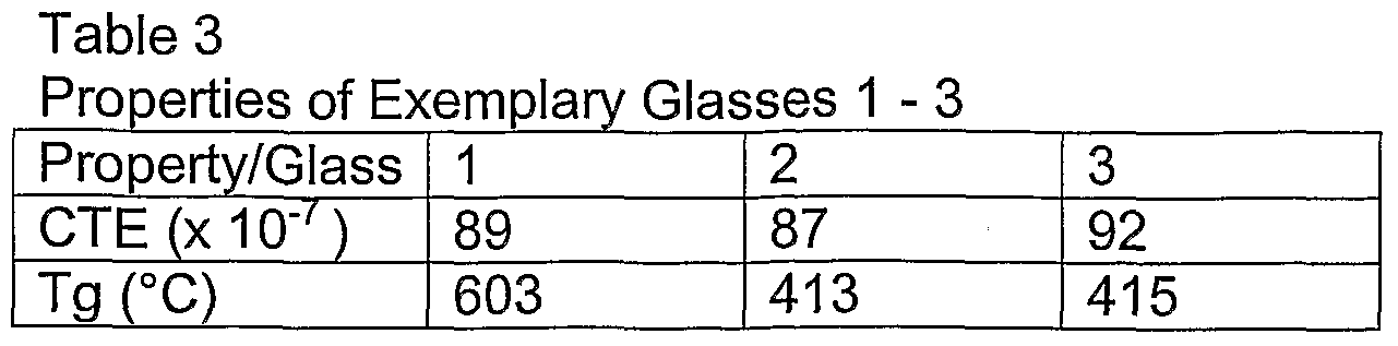
- the paste composition was fired in a N 2 atmosphere on a glass coated 400 series stainless steel at 650 0 C. Selected properties of the glass compositions used in the pastes are found in Table 3. Selected properties of the paste, after firing on glass coated stainless steel, are in Table 4.
- Example 2 [0047] The inventive thick film paste of Example 1 was fired in an N 2 atmosphere on a 96% alumina substrate at 650 0 C. Selected properties of the first paste after firing are listed in Table 4. An SEM cross section of the copper-alumina interface revealed that a thin ( ⁇ 1 ⁇ m) interfacial glass layer forms in between copper and the substrate. It appears that the interfacial glass, derived from the paste, wets and spreads well on both Cu grains and AI 2 O 3 grains without cracking. Energy dispersive x-ray (EDAX) analysis shows a slight dissolution of the substrate alumina into the glass at the glass/alumina interface, which may lead to superior chemical bonding with the substrate.
- EDAX Energy dispersive x-ray
- Example 3 The inventive thick film paste of Example 1 was fired in an N 2 atmosphere on a 96% alumina substrate at 850°C. Selected properties of the paste after firing are listed in Table 4. A slight drop in adhesion after 850 0 C firing as compared to 650 0 C may be due to a thicker interfacial glass layer (6 ⁇ m versus 1 ⁇ m) that was observed. As in 65O 0 C firing, an interfacial glass layer forms in between copper and alumina after 850 0 C firing. Again, the glass shows excellent wetting and spreading over both copper and alumina grains without any delamination or cracking.
- the glasses of the thick print system are designed to limit the formation of a thick interfacial glass layer that may degrade adhesion when fired at high temperatures, e.g., 850 0 C. Good wetting of the copper by the 62Sn/36Pb/2Ag solder was experienced. The copper layer appears very dense.
- Example 4 [0049] The inventive thick film paste of Example 1 was used for the aluminum wire bonding application. Table 4 shows the properties after firing at 850 0 C on a 96% alumina substrate. This copper also has good solder wetting properties. The 0.010" aluminum wires was investigated and found to be due to breakage of the wire but not at the thick film copper/AI 2 O 3 interface affirming the good adhesion between thick print copper and alumina substrate. The paste also exhibits good adhesion when soldered with 22 AWG t in-plated c opper wire. T he failure m anifests b y t he s older I eaving a large area of thick print copper on the alumina substrate. Table 4, specifically columns 2 and 4 reveal that a copper paste can be fired on alumina substrate at the extremes of 650 0 C or 850 0 C, and in either case afford very good mechanical and electrical properties. Table 4. Properties of fired copper pastes
- the thick film pastes of the present invention may be utilized in conjunction with a variety of substrates, including but not limited to porcelain enamel coated steel, beryllia substrates, glass substrates, barium titanate substrates, aluminum nitride substrates and silicon carbide substrates. Additionally, it will be appreciated that in addition to the screen printing technique utilized in the previous Examples, the thick film pastes of the present invention may be applied using a variety of additional techniques known in the art including spraying, brushing, dipping, ink-jet or doctor blade.
Landscapes
- Chemical & Material Sciences (AREA)
- Engineering & Computer Science (AREA)
- Materials Engineering (AREA)
- Organic Chemistry (AREA)
- Chemical Kinetics & Catalysis (AREA)
- General Chemical & Material Sciences (AREA)
- Geochemistry & Mineralogy (AREA)
- Life Sciences & Earth Sciences (AREA)
- Ceramic Engineering (AREA)
- Structural Engineering (AREA)
- Inorganic Chemistry (AREA)
- Dispersion Chemistry (AREA)
- Physics & Mathematics (AREA)
- Spectroscopy & Molecular Physics (AREA)
- Microelectronics & Electronic Packaging (AREA)
- Glass Compositions (AREA)
- Conductive Materials (AREA)
- Non-Adjustable Resistors (AREA)
- Manufacturing Of Printed Wiring (AREA)
- Parts Printed On Printed Circuit Boards (AREA)
Abstract
Description



Claims
Priority Applications (7)
| Application Number | Priority Date | Filing Date | Title |
|---|---|---|---|
| DK05735324.5T DK1784367T3 (en) | 2004-06-09 | 2005-04-15 | Lead-free and cadmium-free conductive thick film pastes |
| CN2005800188236A CN101309874B (en) | 2004-06-09 | 2005-04-15 | Lead-free and cadmium-free conductive copper thick film paste |
| ES05735324T ES2783985T3 (en) | 2004-06-09 | 2005-04-15 | Lead and cadmium free conductive thick film pastes |
| JP2007527233A JP4916442B2 (en) | 2004-06-09 | 2005-04-15 | Lead-free and cadmium-free conductive copper thick film paste |
| KR1020067025694A KR101154928B1 (en) | 2004-06-09 | 2005-04-15 | Lead-free and cadmium-free conductive copper thick film pastes |
| EP05735324.5A EP1784367B1 (en) | 2004-06-09 | 2005-04-15 | Lead-free and cadmium-free conductive thick film pastes |
| CA2566279A CA2566279C (en) | 2004-06-09 | 2005-04-15 | Lead-free and cadmium-free conductive copper thick film pastes |
Applications Claiming Priority (2)
| Application Number | Priority Date | Filing Date | Title |
|---|---|---|---|
| US10/864,304 US7176152B2 (en) | 2004-06-09 | 2004-06-09 | Lead-free and cadmium-free conductive copper thick film pastes |
| US10/864,304 | 2004-06-09 |
Publications (2)
| Publication Number | Publication Date |
|---|---|
| WO2006001882A2 true WO2006001882A2 (en) | 2006-01-05 |
| WO2006001882A3 WO2006001882A3 (en) | 2007-12-13 |
Family
ID=35461252
Family Applications (1)
| Application Number | Title | Priority Date | Filing Date |
|---|---|---|---|
| PCT/US2005/012743 Ceased WO2006001882A2 (en) | 2004-06-09 | 2005-04-15 | Lead-free and cadmium-free conductive copper thick film pastes |
Country Status (10)
| Country | Link |
|---|---|
| US (2) | US7176152B2 (en) |
| EP (1) | EP1784367B1 (en) |
| JP (1) | JP4916442B2 (en) |
| KR (1) | KR101154928B1 (en) |
| CN (1) | CN101309874B (en) |
| CA (1) | CA2566279C (en) |
| DK (1) | DK1784367T3 (en) |
| ES (1) | ES2783985T3 (en) |
| HU (1) | HUE048920T2 (en) |
| WO (1) | WO2006001882A2 (en) |
Cited By (2)
| Publication number | Priority date | Publication date | Assignee | Title |
|---|---|---|---|---|
| JP2008162848A (en) * | 2006-12-28 | 2008-07-17 | Central Glass Co Ltd | Glass ceramic material for plasma display |
| EP3824481A4 (en) * | 2018-09-07 | 2022-08-03 | Ferro Corporation | THICK FILM CONDUCTIVE PASTE FOR SILICON NITRIDE AND OTHER SUBSTRATES |
Families Citing this family (70)
| Publication number | Priority date | Publication date | Assignee | Title |
|---|---|---|---|---|
| US7176152B2 (en) * | 2004-06-09 | 2007-02-13 | Ferro Corporation | Lead-free and cadmium-free conductive copper thick film pastes |
| WO2006003755A1 (en) * | 2004-07-06 | 2006-01-12 | Murata Manufacturing.Co., Ltd. | Electroconductive paste and ceramic electronic parts using the same |
| US7611645B2 (en) * | 2005-04-25 | 2009-11-03 | E. I. Du Pont De Nemours And Company | Thick film conductor compositions and the use thereof in LTCC circuits and devices |
| US8093491B2 (en) * | 2005-06-03 | 2012-01-10 | Ferro Corporation | Lead free solar cell contacts |
| CN101263004B (en) * | 2005-09-14 | 2013-03-27 | 费罗公司 | Extended firing range enamels to produce frost effects |
| JP2007194122A (en) * | 2006-01-20 | 2007-08-02 | Sumitomo Electric Ind Ltd | Conductive paste and wiring board using the same |
| US7547369B2 (en) * | 2006-08-31 | 2009-06-16 | Ferro Corporation | Method of making multilayer structures using tapes on non-densifying substrates |
| US8125060B2 (en) | 2006-12-08 | 2012-02-28 | Infineon Technologies Ag | Electronic component with layered frame |
| JP4291857B2 (en) * | 2007-01-24 | 2009-07-08 | 三ツ星ベルト株式会社 | Copper conductor paste, conductor circuit board and electronic components |
| ES2651625T3 (en) * | 2007-04-25 | 2018-01-29 | Heraeus Precious Metals North America Conshohocken Llc | Formulations for thick film conductors, comprising silver and nickel or silver and nickel alloys and solar cells manufactured therefrom |
| KR100870832B1 (en) * | 2007-05-01 | 2008-11-27 | 대주전자재료 주식회사 | Method for manufacturing barium-based conductive powder for lead-free thick film resist paste |
| US8309844B2 (en) * | 2007-08-29 | 2012-11-13 | Ferro Corporation | Thick film pastes for fire through applications in solar cells |
| US8236598B2 (en) * | 2007-08-31 | 2012-08-07 | Ferro Corporation | Layered contact structure for solar cells |
| US20090266409A1 (en) * | 2008-04-28 | 2009-10-29 | E.I.Du Pont De Nemours And Company | Conductive compositions and processes for use in the manufacture of semiconductor devices |
| KR20110014675A (en) * | 2008-05-28 | 2011-02-11 | 이 아이 듀폰 디 네모아 앤드 캄파니 | Compositions containing submicron particles used in photovoltaic conductors |
| JP2015018814A (en) * | 2010-01-25 | 2015-01-29 | 日立化成株式会社 | Electrode paste composition and solar cell |
| JP5633285B2 (en) * | 2010-01-25 | 2014-12-03 | 日立化成株式会社 | Electrode paste composition and solar cell |
| US9390829B2 (en) | 2010-01-25 | 2016-07-12 | Hitachi Chemical Company, Ltd. | Paste composition for electrode and photovoltaic cell |
| US20120006395A1 (en) * | 2010-07-08 | 2012-01-12 | E. I. Du Pont De Nemours And Company | Coated stainless steel substrate |
| JP5888493B2 (en) * | 2011-02-10 | 2016-03-22 | セントラル硝子株式会社 | Conductive paste and solar cell element using the conductive paste |
| EP2691963B1 (en) * | 2011-03-29 | 2015-02-18 | Sun Chemical Corporation | High-aspect ratio screen printable thick film paste compositions containing wax thixotropes |
| CN102276148B (en) * | 2011-05-26 | 2013-05-22 | 云梦县迪普实业有限公司 | Preparation method of insulating dielectric slurry for stainless steel thick film |
| US20140130940A1 (en) * | 2011-06-08 | 2014-05-15 | Senju Metal Industry Co., Ltd. | Solder Paste |
| JP5176159B1 (en) * | 2011-07-19 | 2013-04-03 | 日立化成株式会社 | N-type diffusion layer forming composition, n-type diffusion layer manufacturing method, and solar cell element manufacturing method |
| TW201318995A (en) * | 2011-08-31 | 2013-05-16 | Nihon Yamamura Glass Co Ltd | Lead-free glass composition for conductor formation |
| DE112012004085T5 (en) * | 2011-09-29 | 2014-07-31 | Noritake Co., Ltd. | Lead-free conductive paste composition for solar cells |
| US20130160812A1 (en) * | 2011-12-22 | 2013-06-27 | E I Du Pont De Nemours And Company | Back contact photovoltaic module with integrated glass back-sheet |
| AT512525B1 (en) | 2012-05-04 | 2013-09-15 | Mikroelektronik Ges Mit Beschraenkter Haftung Ab | Printed circuit board, in particular for a power electronics module, comprising an electrically conductive substrate |
| US20130319496A1 (en) * | 2012-06-01 | 2013-12-05 | Heraeus Precious Metals North America Conshohocken Llc | Low-metal content electroconductive paste composition |
| EP2706538A3 (en) * | 2012-09-10 | 2014-04-23 | Heraeus Precious Metals North America Conshohocken LLC | Low firing temperature copper composition |
| US9236155B2 (en) * | 2013-02-04 | 2016-01-12 | E I Du Pont De Nemours And Company | Copper paste composition and its use in a method for forming copper conductors on substrates |
| US9048222B2 (en) | 2013-03-06 | 2015-06-02 | Taiwan Semiconductor Manufacturing Company, Ltd. | Method of fabricating interconnect structure for package-on-package devices |
| US9351398B2 (en) | 2013-04-04 | 2016-05-24 | GM Global Technology Operations LLC | Thick film conductive inks for electronic devices |
| US9637409B2 (en) | 2013-04-18 | 2017-05-02 | Ferro Corporation | Low melting glass compositions |
| DE102013105304A1 (en) * | 2013-05-23 | 2014-11-27 | Osram Opto Semiconductors Gmbh | Process for the preparation of a powdery precursor material, powdery precursor material and its use |
| US9799421B2 (en) * | 2013-06-07 | 2017-10-24 | Heraeus Precious Metals North America Conshohocken Llc | Thick print copper pastes for aluminum nitride substrates |
| CN104240841A (en) * | 2013-06-14 | 2014-12-24 | 中国振华集团云科电子有限公司 | Base metal conductor paste preparation method |
| EP2824672B1 (en) * | 2013-07-09 | 2017-08-30 | Heraeus Deutschland GmbH & Co. KG | An electro-conductive paste comprising Ag particles with a multimodal diameter distribution in the preparation of electrodes in MWT solar cells |
| US9681559B2 (en) | 2013-12-19 | 2017-06-13 | GM Global Technology Operations LLC | Thick film circuits with conductive components formed using different conductive elements and related methods |
| US9583420B2 (en) | 2015-01-23 | 2017-02-28 | Taiwan Semiconductor Manufacturing Company, Ltd. | Semiconductor device and method of manufactures |
| US9281297B2 (en) | 2014-03-07 | 2016-03-08 | Taiwan Semiconductor Manufacturing Company, Ltd. | Solution for reducing poor contact in info packages |
| KR101940981B1 (en) | 2014-05-05 | 2019-01-23 | 3디 글래스 솔루션즈 인코포레이티드 | 2d and 3d inductors antenna and transformers fabricating photoactive substrates |
| US9449947B2 (en) | 2014-07-01 | 2016-09-20 | Taiwan Semiconductor Manufacturing Company, Ltd. | Semiconductor package for thermal dissipation |
| WO2016140351A1 (en) * | 2015-03-05 | 2016-09-09 | 国立大学法人大阪大学 | Method for producing copper particles, copper particles and copper paste |
| US20190177213A1 (en) * | 2016-01-31 | 2019-06-13 | 3D Glass Solutions, Inc. | Multi-Layer Photo Definable Glass with Integrated Devices |
| EP3356304B1 (en) | 2016-02-19 | 2020-06-10 | Ferro Corporation | Sintering aid glasses for machinable phyllosilicate based structures |
| US12165809B2 (en) | 2016-02-25 | 2024-12-10 | 3D Glass Solutions, Inc. | 3D capacitor and capacitor array fabricating photoactive substrates |
| KR20200010598A (en) | 2016-02-25 | 2020-01-30 | 3디 글래스 솔루션즈 인코포레이티드 | 3d capacitor and capacitor array fabricating photoactive substrates |
| RU2614818C1 (en) * | 2016-03-15 | 2017-03-29 | Юлия Алексеевна Щепочкина | Glaze |
| WO2017177171A1 (en) | 2016-04-08 | 2017-10-12 | 3D Glass Solutions, Inc. | Methods of fabricating photosensitive substrates suitable for optical coupler |
| KR101848694B1 (en) * | 2017-02-13 | 2018-04-16 | 대주전자재료 주식회사 | Lead-free thick film resistor, and electronic deivce coprising the same |
| JP6931455B2 (en) * | 2017-02-17 | 2021-09-08 | 住友金属鉱山株式会社 | A composition for a resistor, a resistor paste containing the same, and a thick film resistor using the same. |
| WO2018200804A1 (en) | 2017-04-28 | 2018-11-01 | 3D Glass Solutions, Inc. | Rf circulator |
| WO2019005452A1 (en) * | 2017-06-29 | 2019-01-03 | Heraeus Precious Metals North America Conshohocken Llc | Copper-containing thick print electroconductive pastes |
| AU2018297035B2 (en) | 2017-07-07 | 2021-02-25 | 3D Glass Solutions, Inc. | 2D and 3D RF lumped element devices for RF system in a package photoactive glass substrates |
| WO2019118761A1 (en) | 2017-12-15 | 2019-06-20 | 3D Glass Solutions, Inc. | Coupled transmission line resonate rf filter |
| KR102600200B1 (en) | 2018-01-04 | 2023-11-10 | 3디 글래스 솔루션즈 인코포레이티드 | Impedance matching conductive structure for high-efficiency RF circuits |
| KR102145746B1 (en) | 2018-04-10 | 2020-08-19 | 3디 글래스 솔루션즈 인코포레이티드 | RF integrated power conditioning capacitor |
| GB201806411D0 (en) * | 2018-04-19 | 2018-06-06 | Johnson Matthey Plc | Kit, particle mixture, paste and methods |
| KR102475010B1 (en) | 2018-05-29 | 2022-12-07 | 3디 글래스 솔루션즈 인코포레이티드 | Low insertion loss rf transmission line |
| GB201812052D0 (en) * | 2018-07-24 | 2018-09-05 | Johnson Matthey Plc | Particle mixture, kit, ink, methods and article |
| KR102518025B1 (en) | 2018-09-17 | 2023-04-06 | 3디 글래스 솔루션즈 인코포레이티드 | High efficiency compact slotted antenna with a ground plane |
| JP7241433B2 (en) | 2018-12-28 | 2023-03-17 | スリーディー グラス ソリューションズ,インク | Heterogeneous Integration for RF, Microwave and MM Wave Systems on Photoactive Glass Substrates |
| WO2020139955A1 (en) | 2018-12-28 | 2020-07-02 | 3D Glass Solutions, Inc. | Annular capacitor rf, microwave and mm wave systems |
| WO2020206323A1 (en) | 2019-04-05 | 2020-10-08 | 3D Glass Solutions, Inc. | Glass based empty substrate integrated waveguide devices |
| WO2020214788A1 (en) | 2019-04-18 | 2020-10-22 | 3D Glass Solutions, Inc. | High efficiency die dicing and release |
| WO2021211855A1 (en) | 2020-04-17 | 2021-10-21 | 3D Glass Solutions, Inc. | Broadband inductor |
| WO2022160136A1 (en) * | 2021-01-27 | 2022-08-04 | 深圳麦克韦尔科技有限公司 | Ceramic matrix and preparation method therefor, ceramic heating element and electronic atomization device |
| CN114477994A (en) * | 2022-01-25 | 2022-05-13 | 广东爱晟电子科技有限公司 | High-power ceramic chip resistor and material and preparation thereof |
| CN119707302B (en) * | 2025-02-28 | 2025-08-29 | 西安腾星电子科技有限公司 | Application of Beryllium Oxide in Slurry Development |
Citations (1)
| Publication number | Priority date | Publication date | Assignee | Title |
|---|---|---|---|---|
| US5114885A (en) | 1991-04-16 | 1992-05-19 | E. I. Du Pont De Nemours And Company | Encapsulant composition |
Family Cites Families (39)
| Publication number | Priority date | Publication date | Assignee | Title |
|---|---|---|---|---|
| US3615772A (en) | 1969-04-25 | 1971-10-26 | Owens Illinois Inc | Fluorine-containing borate glass compositions |
| FR2388381A1 (en) | 1976-12-27 | 1978-11-17 | Labo Electronique Physique | DIELECTRIC COMPOSITION, SCREENABLE DOUGH CONTAINING SUCH COMPOSITION AND PRODUCTS OBTAINED |
| JPS5485399A (en) | 1977-12-21 | 1979-07-06 | Hitachi Ltd | Dielectric paste |
| FR2451899A1 (en) | 1979-03-23 | 1980-10-17 | Labo Electronique Physique | DIELECTRIC COMPOSITION, SERIGRAPHIABLE INK COMPRISING SUCH A COMPOSITION, AND PRODUCTS OBTAINED |
| US4379319A (en) | 1982-02-18 | 1983-04-05 | Ferro Corporation | Monolithic ceramic capacitors and improved ternary ceramic compositions for producing same |
| US4517155A (en) | 1982-05-18 | 1985-05-14 | Union Carbide Corporation | Copper base metal termination for multilayer ceramic capacitors |
| US4880567A (en) | 1987-08-20 | 1989-11-14 | General Electric Company | Thick film copper conductor inks |
| US4906406A (en) | 1988-07-21 | 1990-03-06 | E. I. Du Pont De Nemours And Company | Thermistor composition |
| JPH0764588B2 (en) | 1989-04-28 | 1995-07-12 | 日本電気硝子株式会社 | Glass composition for coating |
| US5296426A (en) | 1990-06-15 | 1994-03-22 | E. I. Du Pont De Nemours And Company | Low-fire X7R compositions |
| US5165986A (en) | 1991-06-05 | 1992-11-24 | Ferro Corporation | Copper conductive composition for use on aluminum nitride substrate |
| FR2687997B1 (en) * | 1992-03-02 | 1996-07-05 | Degussa Prod Ceramiques | GLASS SINTERS CONTAINING ZINC, FREE OF LEAD AND CADMIUM - PROCESS OF MANUFACTURE AND USE. |
| JP3257036B2 (en) * | 1992-06-09 | 2002-02-18 | 三菱マテリアル株式会社 | Conductive paste for chip-type electronic components |
| JPH06349314A (en) * | 1993-06-03 | 1994-12-22 | Murata Mfg Co Ltd | Conductive paste |
| US5378408A (en) | 1993-07-29 | 1995-01-03 | E. I. Du Pont De Nemours And Company | Lead-free thick film paste composition |
| US5439852A (en) | 1994-08-01 | 1995-08-08 | E. I. Du Pont De Nemours And Company | Cadmium-free and lead-free thick film conductor composition |
| US5491118A (en) | 1994-12-20 | 1996-02-13 | E. I. Du Pont De Nemours And Company | Cadmium-free and lead-free thick film paste composition |
| US5948536A (en) | 1996-05-10 | 1999-09-07 | Tdk Corporation | Glass composition for substrates with a built-in lead base dielectric material, and multilayer substrate with a built-in capacitor |
| US5753571A (en) * | 1997-02-13 | 1998-05-19 | E. I. Du Pont De Nemours And Company | Lead and cadmium-free encapsulant composition |
| US5998037A (en) * | 1997-12-22 | 1999-12-07 | Ferro Corporation | Porcelain enamel composition for electronic applications |
| US6171987B1 (en) | 1997-12-29 | 2001-01-09 | Ben-Gurion University Of The Negev | Cadmium-free and lead-free glass compositions, thick film formulations containing them and uses thereof |
| JP3271585B2 (en) | 1998-06-19 | 2002-04-02 | 日本電気株式会社 | Video decoding device |
| JP2000138010A (en) * | 1998-08-26 | 2000-05-16 | Mitsuboshi Belting Ltd | Copper conductor paste |
| US6124224A (en) | 1998-09-02 | 2000-09-26 | Ferro Corporation | High temperature sealing glass |
| JP2000106033A (en) * | 1998-09-28 | 2000-04-11 | Mitsuboshi Belting Ltd | Copper conductor paste |
| US6105394A (en) | 1999-01-12 | 2000-08-22 | Ferro Corporation | Glass enamel for automotive applications |
| US6185087B1 (en) | 1999-04-08 | 2001-02-06 | Kemet Electronics Corp. | Multilayer ceramic chip capacitor with high reliability compatible with nickel electrodes |
| JP2001028207A (en) * | 1999-07-14 | 2001-01-30 | Murata Mfg Co Ltd | Conductive paste and ceramic electronic component |
| US6534346B2 (en) * | 2000-05-16 | 2003-03-18 | Nippon Electric Glass Co., Ltd. | Glass and glass tube for encapsulating semiconductors |
| JP3534684B2 (en) * | 2000-07-10 | 2004-06-07 | Tdk株式会社 | Conductive paste, external electrode and method of manufacturing the same |
| JP4423832B2 (en) * | 2000-09-14 | 2010-03-03 | 昭栄化学工業株式会社 | Glass composition and thick film paste using the same |
| US6673274B2 (en) | 2001-04-11 | 2004-01-06 | Cabot Corporation | Dielectric compositions and methods to form the same |
| US7146155B2 (en) * | 2001-08-03 | 2006-12-05 | Mcafee, Inc. | System and method for providing telephonic content security service in a wireless network environment |
| JP2003124051A (en) * | 2001-10-11 | 2003-04-25 | Kyoto Elex Kk | Paste composition for external electrode of laminated ceramic capacitor |
| JP4300786B2 (en) * | 2001-12-21 | 2009-07-22 | 昭栄化学工業株式会社 | Glass and conductive paste using the same |
| US20030162553A1 (en) * | 2002-02-28 | 2003-08-28 | Huang Ching Yao | Wireless paging based at least partially on the technological capability of the mobile device |
| US6982864B1 (en) * | 2004-06-09 | 2006-01-03 | Ferro Corporation | Copper termination inks containing lead free and cadmium free glasses for capacitors |
| US7176152B2 (en) | 2004-06-09 | 2007-02-13 | Ferro Corporation | Lead-free and cadmium-free conductive copper thick film pastes |
| US7339780B2 (en) * | 2004-06-09 | 2008-03-04 | Ferro Corporation | Copper termination inks containing lead free and cadmium free glasses for capacitors |
-
2004
- 2004-06-09 US US10/864,304 patent/US7176152B2/en not_active Expired - Lifetime
-
2005
- 2005-04-15 HU HUE05735324A patent/HUE048920T2/en unknown
- 2005-04-15 CN CN2005800188236A patent/CN101309874B/en not_active Expired - Fee Related
- 2005-04-15 KR KR1020067025694A patent/KR101154928B1/en not_active Expired - Fee Related
- 2005-04-15 ES ES05735324T patent/ES2783985T3/en not_active Expired - Lifetime
- 2005-04-15 WO PCT/US2005/012743 patent/WO2006001882A2/en not_active Ceased
- 2005-04-15 EP EP05735324.5A patent/EP1784367B1/en not_active Expired - Lifetime
- 2005-04-15 JP JP2007527233A patent/JP4916442B2/en not_active Expired - Fee Related
- 2005-04-15 DK DK05735324.5T patent/DK1784367T3/en active
- 2005-04-15 CA CA2566279A patent/CA2566279C/en not_active Expired - Lifetime
-
2006
- 2006-12-13 US US11/609,998 patent/US7504349B2/en not_active Expired - Lifetime
Patent Citations (1)
| Publication number | Priority date | Publication date | Assignee | Title |
|---|---|---|---|---|
| US5114885A (en) | 1991-04-16 | 1992-05-19 | E. I. Du Pont De Nemours And Company | Encapsulant composition |
Cited By (3)
| Publication number | Priority date | Publication date | Assignee | Title |
|---|---|---|---|---|
| JP2008162848A (en) * | 2006-12-28 | 2008-07-17 | Central Glass Co Ltd | Glass ceramic material for plasma display |
| EP3824481A4 (en) * | 2018-09-07 | 2022-08-03 | Ferro Corporation | THICK FILM CONDUCTIVE PASTE FOR SILICON NITRIDE AND OTHER SUBSTRATES |
| EP4235773A3 (en) * | 2018-09-07 | 2023-10-04 | Ferro Corporation | Conductive thick film paste for silicon nitride and other substrates |
Also Published As
| Publication number | Publication date |
|---|---|
| CA2566279A1 (en) | 2006-01-05 |
| WO2006001882A3 (en) | 2007-12-13 |
| US7504349B2 (en) | 2009-03-17 |
| JP2008504667A (en) | 2008-02-14 |
| EP1784367A4 (en) | 2011-05-25 |
| KR101154928B1 (en) | 2012-07-09 |
| US7176152B2 (en) | 2007-02-13 |
| HUE048920T2 (en) | 2020-08-28 |
| CN101309874A (en) | 2008-11-19 |
| US20070108423A1 (en) | 2007-05-17 |
| CA2566279C (en) | 2011-02-08 |
| EP1784367A2 (en) | 2007-05-16 |
| CN101309874B (en) | 2012-02-15 |
| DK1784367T3 (en) | 2020-03-30 |
| US20050277550A1 (en) | 2005-12-15 |
| JP4916442B2 (en) | 2012-04-11 |
| EP1784367B1 (en) | 2020-01-08 |
| ES2783985T3 (en) | 2020-09-21 |
| KR20070015451A (en) | 2007-02-02 |
Similar Documents
| Publication | Publication Date | Title |
|---|---|---|
| CA2566279C (en) | Lead-free and cadmium-free conductive copper thick film pastes | |
| JP5303552B2 (en) | Conductive paste for ceramic substrate and electric circuit | |
| US5165986A (en) | Copper conductive composition for use on aluminum nitride substrate | |
| EP1717855B1 (en) | Thick film conductor compositions and the use thereof in LTCC circuits and devices | |
| US20100200283A1 (en) | Insulation paste for a metal core substrate and electronic device | |
| EP1505040B1 (en) | Thick film dielectric compositions for use on aluminium nitride substrates | |
| JPH0529616B2 (en) | ||
| US4532075A (en) | Thick film conductor composition | |
| EP3824481B1 (en) | Conductive thick film paste for silicon nitride and other substrates | |
| CN1608298B (en) | Use of Conductor Compounds in Circuits | |
| US4567151A (en) | Binder glass of Bi2 O3 -SiO2 -GeO2 (-PbO optional) admixed with ZnO/ZnO and Bi2 O3 | |
| WO1990000966A1 (en) | Thick film dielectric compositions | |
| US20060009036A1 (en) | High thermal cycle conductor system | |
| JPH06136298A (en) | Low temperature-baking paste for outer conductor of multi layer circuit board having copper inner conductor |
Legal Events
| Date | Code | Title | Description |
|---|---|---|---|
| AK | Designated states |
Kind code of ref document: A2 Designated state(s): AE AG AL AM AT AU AZ BA BB BG BR BW BY BZ CA CH CN CO CR CU CZ DE DK DM DZ EC EE EG ES FI GB GD GE GH GM HR HU ID IL IN IS JP KE KG KM KP KR KZ LC LK LR LS LT LU LV MA MD MG MK MN MW MX MZ NA NI NO NZ OM PG PH PL PT RO RU SC SD SE SG SK SL SM SY TJ TM TN TR TT TZ UA UG US UZ VC VN YU ZA ZM ZW |
|
| AL | Designated countries for regional patents |
Kind code of ref document: A2 Designated state(s): BW GH GM KE LS MW MZ NA SD SL SZ TZ UG ZM ZW AM AZ BY KG KZ MD RU TJ TM AT BE BG CH CY CZ DE DK EE ES FI FR GB GR HU IE IS IT LT LU MC NL PL PT RO SE SI SK TR BF BJ CF CG CI CM GA GN GQ GW ML MR NE SN TD TG |
|
| WWE | Wipo information: entry into national phase |
Ref document number: 2566279 Country of ref document: CA |
|
| WWE | Wipo information: entry into national phase |
Ref document number: 1020067025694 Country of ref document: KR |
|
| WWE | Wipo information: entry into national phase |
Ref document number: 2007527233 Country of ref document: JP |
|
| WWE | Wipo information: entry into national phase |
Ref document number: 200580018823.6 Country of ref document: CN |
|
| NENP | Non-entry into the national phase |
Ref country code: DE |
|
| WWW | Wipo information: withdrawn in national office |
Country of ref document: DE |
|
| WWE | Wipo information: entry into national phase |
Ref document number: 2005735324 Country of ref document: EP |
|
| WWP | Wipo information: published in national office |
Ref document number: 1020067025694 Country of ref document: KR |
|
| WWP | Wipo information: published in national office |
Ref document number: 2005735324 Country of ref document: EP |