WO2008044411A1 - Dispositif à ondes limites élastiques - Google Patents
Dispositif à ondes limites élastiques Download PDFInfo
- Publication number
- WO2008044411A1 WO2008044411A1 PCT/JP2007/067583 JP2007067583W WO2008044411A1 WO 2008044411 A1 WO2008044411 A1 WO 2008044411A1 JP 2007067583 W JP2007067583 W JP 2007067583W WO 2008044411 A1 WO2008044411 A1 WO 2008044411A1
- Authority
- WO
- WIPO (PCT)
- Prior art keywords
- thickness
- electrode
- dielectric layer
- group
- substrate
- Prior art date
- Legal status (The legal status is an assumption and is not a legal conclusion. Google has not performed a legal analysis and makes no representation as to the accuracy of the status listed.)
- Ceased
Links
Classifications
-
- H—ELECTRICITY
- H03—ELECTRONIC CIRCUITRY
- H03H—IMPEDANCE NETWORKS, e.g. RESONANT CIRCUITS; RESONATORS
- H03H9/00—Networks comprising electromechanical or electro-acoustic elements; Electromechanical resonators
- H03H9/02—Details
- H03H9/0222—Details of interface-acoustic, boundary, pseudo-acoustic or Stonely wave devices
-
- H—ELECTRICITY
- H03—ELECTRONIC CIRCUITRY
- H03H—IMPEDANCE NETWORKS, e.g. RESONANT CIRCUITS; RESONATORS
- H03H3/00—Apparatus or processes specially adapted for the manufacture of impedance networks, resonating circuits, resonators
- H03H3/007—Apparatus or processes specially adapted for the manufacture of impedance networks, resonating circuits, resonators for the manufacture of electromechanical resonators or networks
- H03H3/08—Apparatus or processes specially adapted for the manufacture of impedance networks, resonating circuits, resonators for the manufacture of electromechanical resonators or networks for the manufacture of resonators or networks using surface acoustic waves
-
- H—ELECTRICITY
- H03—ELECTRONIC CIRCUITRY
- H03H—IMPEDANCE NETWORKS, e.g. RESONANT CIRCUITS; RESONATORS
- H03H9/00—Networks comprising electromechanical or electro-acoustic elements; Electromechanical resonators
- H03H9/02—Details
- H03H9/02535—Details of surface acoustic wave devices
- H03H9/02543—Characteristics of substrate, e.g. cutting angles
- H03H9/02559—Characteristics of substrate, e.g. cutting angles of lithium niobate or lithium-tantalate substrates
-
- H—ELECTRICITY
- H03—ELECTRONIC CIRCUITRY
- H03H—IMPEDANCE NETWORKS, e.g. RESONANT CIRCUITS; RESONATORS
- H03H9/00—Networks comprising electromechanical or electro-acoustic elements; Electromechanical resonators
- H03H9/02—Details
- H03H9/02535—Details of surface acoustic wave devices
- H03H9/02637—Details concerning reflective or coupling arrays
- H03H9/02653—Grooves or arrays buried in the substrate
- H03H9/02661—Grooves or arrays buried in the substrate being located inside the interdigital transducers
-
- H—ELECTRICITY
- H03—ELECTRONIC CIRCUITRY
- H03H—IMPEDANCE NETWORKS, e.g. RESONANT CIRCUITS; RESONATORS
- H03H9/00—Networks comprising electromechanical or electro-acoustic elements; Electromechanical resonators
- H03H9/02—Details
- H03H9/02535—Details of surface acoustic wave devices
- H03H9/02818—Means for compensation or elimination of undesirable effects
- H03H9/02834—Means for compensation or elimination of undesirable effects of temperature influence
-
- H—ELECTRICITY
- H10—SEMICONDUCTOR DEVICES; ELECTRIC SOLID-STATE DEVICES NOT OTHERWISE PROVIDED FOR
- H10N—ELECTRIC SOLID-STATE DEVICES NOT OTHERWISE PROVIDED FOR
- H10N30/00—Piezoelectric or electrostrictive devices
- H10N30/20—Piezoelectric or electrostrictive devices with electrical input and mechanical output, e.g. functioning as actuators or vibrators
-
- H—ELECTRICITY
- H10—SEMICONDUCTOR DEVICES; ELECTRIC SOLID-STATE DEVICES NOT OTHERWISE PROVIDED FOR
- H10N—ELECTRIC SOLID-STATE DEVICES NOT OTHERWISE PROVIDED FOR
- H10N30/00—Piezoelectric or electrostrictive devices
- H10N30/80—Constructional details
- H10N30/85—Piezoelectric or electrostrictive active materials
Definitions
- the present invention relates to a boundary acoustic wave device used as, for example, a resonator or a bandpass filter. More specifically, the present invention relates to a piezoelectric body, an electrode formed by embedding metal in the upper surface of the piezoelectric body, The present invention relates to a boundary acoustic wave device having a dielectric provided so as to cover an electrode.
- Duplexers (DPX) and RF filters used in mobile communication systems are required to satisfy both broadband and good temperature characteristics.
- surface acoustic wave devices used for DPX and RF filters use a piezoelectric substrate consisting of a 36 °, 50 ° rotated Y plate, X propagation LiTaO force, and so on.
- This piezoelectric substrate had a frequency temperature coefficient of about 45 35 ppm / ° C.
- a method of forming a SiO film having a positive frequency temperature coefficient so as to cover an IDT electrode on a piezoelectric substrate is known.
- Non-Patent Document 1 shows an ID on a LiNbO substrate.
- a boundary acoustic wave filter device comprising a T electrode and a SiO film as a dielectric formed in this order.
- the sound velocity of the SH boundary acoustic wave propagating through the boundary between the SiO film and the SiO film is lower than the slow transverse wave of the SiO film. Comb, SH boundary wave is not leaked.
- the thickness of the IDT electrode where non-leakage of the SH type boundary wave is as shown in Fig. 3 of Non-Patent Document 1. In the case of electrodes, it is set to 0.04 ⁇ or more. ⁇ represents the wavelength of the SH boundary wave.
- Non-patent document 1 "RF filter using boundary acoustic wave” (Proc. Symp. Ultrason. Electr on., Vol. 26, pp. 25- 26 (2005/11))
- An object of the present invention is to effectively confine an SH-type boundary acoustic wave at the boundary between a piezoelectric body and a dielectric body even in the case where the thickness of the electrode is reduced in view of the current state of the prior art described above. It is another object of the present invention to provide a boundary acoustic wave device with low loss.
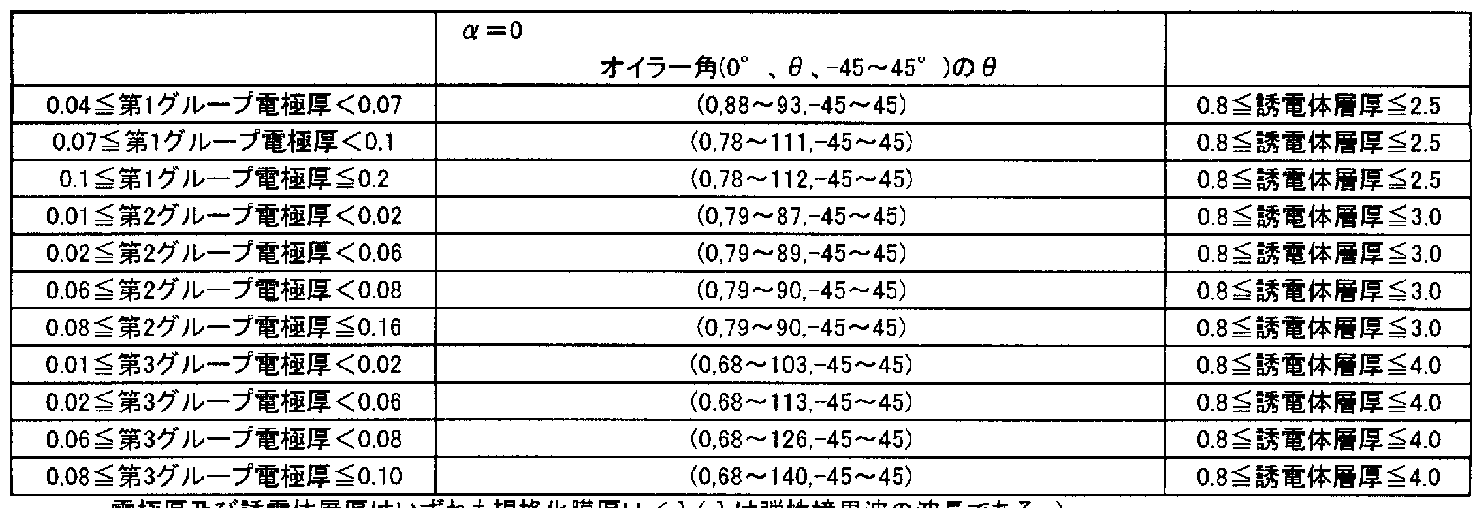
- a LiNbO substrate having an Euler angle (0 °, ⁇ , -45 ° to + 45 °) having a plurality of grooves formed on the upper surface, and a metal material in the grooves Is filled and formed
- the dielectric layer has a flat upper surface, and the metal material forming the electrode is selected from Al, Ti, Ni, Cr, Cu, W, Ta, Pt, Ag and Au A1 and Ti are the first group, Ni and Cr are the second group, Cu, W, Ta, Pt, Ag and Au are the third group. Table 1 below shows the thickness of the electrode, the Euler angle ⁇ of the LiNbO substrate, and the thickness of the dielectric layer.
- a boundary acoustic wave device is provided that is in any of the above ranges.
- the Euler angle ⁇ of the plate and the thickness of the dielectric layer are within one of the ranges shown in Table 2 below.
- the upper surface of the dielectric layer is flat, and the metal material forming the electrode is one of Al, Cu, Au, Ta, and Pt, and the thickness of the electrode, the LiTaO Base
- a boundary acoustic wave device is provided in which the Euler angle ⁇ of the plate and the thickness of the dielectric layer are in any of the ranges shown in Table 3 below.
- the electrode thickness and the dielectric layer are both normalized boundary acoustic waves.
- the thickness of the electrode and the thickness of the LiTaO substrate are the same.
- the thickness of the dielectric layer ⁇ and the dielectric layer is within one of the ranges shown in Table 4 below:
- Electrode thickness and dielectric layer ! are Electrode thickness and dielectric layer !?
- the normalized film thickness is the wave of the sex boundary wave.
- the dielectric layer is made of silicon oxide.
- the frequency temperature coefficient TCF is positive and the frequency of LiNbO and LiTaO
- the temperature coefficient TCF is a negative value, it is possible to provide a boundary acoustic wave device having a small temperature temperature coefficient and a good temperature characteristic.
- the groove formed on the upper surface of the LiNbO substrate is made of gold.
- An electrode is filled with a metal material, and a dielectric material covers the LiNbO substrate and the electrode.
- the thickness of the electrode can be adjusted by adjusting the depth of the groove. Therefore, it is difficult for a step between the portion where the electrode exists and the portion where the electrode does not exist to occur. Therefore, the upper surface of the dielectric layer can be easily flattened, and insertion loss can be reduced.
- the metal material forming the electrode includes a first group, a second group, and a second group.
- the thickness of the dielectric layer and the thickness of the electrode are shown in Table 1 within the range of! /, Ru! /, And as shown in the specific experimental examples described later, the electrode Even when the thickness of the SH-type boundary wave is reduced, the SH-type boundary wave can be made non-leakage, which makes it possible to provide a low-loss boundary acoustic wave device using the SH-type boundary wave. Become.
- the groove formed in the upper surface of the LiTaO substrate is filled with the metal material.
- An electrode is formed, and a dielectric layer is formed to cover the LiTaO substrate and the electrode.
- the electrode forming material is one of the metal materials of Al, Cu, Au, Ta, and Pt, and the electrode thickness, Euler angle ⁇ of the LiTaO substrate, and the dielectric layer Thickness
- the SH boundary wave can be made non-leakage. This makes it possible to provide a low-loss boundary acoustic wave device using SH-type boundary waves.
- the loss of the boundary acoustic wave device can be further reduced. it can.
- FIG. 1 (a) to (f) are front sectional views for explaining a method and a structure for manufacturing a boundary acoustic wave device according to an embodiment of the present invention.
- FIG. 2 is a plan view schematically showing an electrode structure of the boundary acoustic wave device according to the embodiment shown in FIG. 1. 3)
- Figure 3 shows the boundary acoustic wave device of the present embodiment, in which grooves are formed on a LiNbO substrate with Euler angles (0 °, 103 °, 0 °), and the grooves are filled with A or Ti. Structure with electrodes
- FIG. 6 is a diagram showing the relationship between the normalized film thickness H / ⁇ of the electrode of the manufactured boundary acoustic wave device and the attenuation constant ⁇ .
- FIG. 4 shows a boundary acoustic wave device according to the present embodiment in which grooves are formed on a LiNbO substrate with Euler angles (0 °, 103 °, 0 °), and the grooves are filled with N or Cr. Structure with electrodes formed
- FIG. 6 is a diagram showing the relationship between the normalized film thickness H / ⁇ of the electrode of the manufactured boundary acoustic wave device and the attenuation constant ⁇ .
- FIG. 5 is a diagram illustrating the boundary acoustic wave device according to the present embodiment in which grooves are formed on a LiNbO substrate with Euler angles (0 °, 103 °, 0 °), and each metal material of the third group is formed in the grooves.
- Figure 6 shows the change in Euler angle ⁇ of LiNbO substrate and the normalized film thickness of A
- Figure 7 shows the change in Euler angle ⁇ of LiNbO substrate and the normalized film thickness of the electrode made of Ni.
- Fig. 8 shows changes in Euler angle ⁇ of LiNbO substrate and normalized film thickness of Cu electrodes.
- FIG. 9 shows an A1 force in a groove provided in a LiNbO substrate with Euler angles (0 °, 103., 0 °).
- FIG. 1 A first figure.
- FIG. 10 shows a case where Ni is formed in a groove provided in a EuN angle (0 °, 103., 0 °) LiNbO substrate.
- FIG. 1 A first figure.
- FIG. 11 shows Cu in a groove provided on a EuN angle (0 °, 103., 0 °) LiNbO substrate.
- FIG. 1 A first figure.
- FIG. 12 shows the SiO film in the laminated structure of SiO / embedded IDT electrode / LiNbO.
- 2 3 2 is a schematic diagram schematically showing the energy distribution of elastic waves when the normalized film thickness ⁇ / ⁇ is less than 0.8.
- FIG. 13 shows the SiO film in a laminated structure of SiO / embedded IDT electrode / LiNbO.
- 2 3 2 is a schematic diagram schematically showing the energy distribution of elastic waves when the normalized film thickness ⁇ / ⁇ is 0.8 or more.
- FIG. 14 shows the SiO force and the thickness of a dielectric layer of 1 in the boundary acoustic wave device of the first embodiment and the comparative boundary acoustic wave device having a non-embedded IDT electrode.
- FIG. 6 is a diagram showing frequency temperature coefficients TCF when ⁇ or 2 ⁇ is set.
- Fig. 15 shows the Euler angles when EuTa angles (0 °, ⁇ , 0) are used.
- FIG. 5 is a diagram showing the relationship between ⁇ , the thickness of A1 constituting the IDT electrode, and the damping constant ⁇ of the boundary acoustic wave device.
- Figure 16 shows the Euler angles when using EuTa angles (0 °, ⁇ , 0) LiTaO.
- Fig. 17 shows the Euler angles when using EuTa angles (0 °, ⁇ , 0) LiTaO.
- FIG. 6 is a diagram showing the relationship between ⁇ , the film thickness of Au constituting the IDT electrode, and the attenuation constant ⁇ of the boundary acoustic wave device.
- Figure 18 shows the Euler angles when using Euler angles (0 °, ⁇ , 0) LiTaO.
- FIG. 6 is a diagram showing the relationship between ⁇ , the thickness of Ta constituting the IDT electrode, and the damping constant ⁇ of the boundary acoustic wave device.
- Fig.19 shows the Euler angles when using Euler angles (0 °, ⁇ , 0) LiTaO.
- Fig.20 shows the embedded type of LiTaO with Euler angles (0 °, 126 °, 0 °)
- the normalized film thickness ⁇ / ⁇ of SiO and A1 And the normalized film thickness is a diagram showing the relationship between the electromechanical coupling factor k 2.
- Fig.21 shows the embedding of Au in LiTaO with Euler angles (0 °, 126 °, 0 °)
- Fig.22 shows Cu embedded in LiTaO with Euler angles (0 °, 126 °, 0 °)
- Type electrode and the standardized film thickness ⁇ / ⁇ of Cu in the structure where SiO is laminated, Cu
- Fig.23 shows Ta embedded in LiTaO with Euler angles (0 °, 126 °, 0 °)
- Figure 24 shows the embedded type made of Pt in LiTaO with Euler angles (0 °, 126 °, 0 °)
- the normalized film thickness is a diagram showing the relationship between the electromechanical coupling factor k 2.
- a boundary acoustic wave device according to an embodiment of the present invention is manufactured.
- the structure of the boundary acoustic wave device will be clarified by explaining the manufacturing method.
- a LiNbO substrate is prepared as a piezoelectric substrate.
- a photoresist layer 2 is formed on the entire upper surface la of the LiNbO substrate 1.
- an appropriate photoresist material that can withstand reactive ion etching (RIE) to be performed later can be used.
- RIE reactive ion etching
- the thickness of the photoresist layer 2 was 2 m.
- the photoresist layer was exposed and developed to pattern the photoresist layer 2 to form a photoresist pattern 2A, as shown in FIG. 1 (b).
- the photoresist layer is removed in a portion where an IDT electrode is formed later.
- etching was performed to form a plurality of grooves lb having a desired depth on the upper surface la of the LiNbO substrate 1 as shown in FIG. 1 (c).
- This desired depth is the same dimension as the film thickness of an IDT electrode to be formed later.
- the etching depth may be slightly larger or smaller than the film thickness dimension of the IDT electrode.
- an A1 film was formed by vapor deposition or sputtering. As a result, as shown in FIG. 1 (d), the A1 film, that is, the electrode film 3 was filled in the groove lb. Note that the A1 film remains
- the LiNbO substrate was immersed in a stripping solution such as acetone, and the A1 film on the photoresist pattern 2A and the photoresist pattern 2A was removed.
- the electrode film 3 is filled in the groove lb, and the upper surface is almost flush with the LiNbO substrate.
- an SiO film 4 was formed as a dielectric layer on the upper surface to obtain an elastic boundary wave device 5.
- the surface of the SiO film 4 is planarized. This is because the upper surface la of the underlying LiNb O substrate 1 and the upper surface of the electrode film 3 are almost flush with each other and are almost flattened. This is because the surface of the SiO film 4 can be surely flattened.
- the method of forming the SiO film 4 is not particularly limited, and is a printing method, vapor deposition, or sputtering. It can be performed by an appropriate method such as.
- the electrode film 3 forms an electrode structure including an IDT electrode.
- the electrode structure is not particularly limited.
- a 1-port boundary acoustic wave resonator 11 shown in a plan view in FIG. 2 may be configured.
- reflectors 12 and 13 force S are also formed by the electrode film on both sides of boundary acoustic wave propagation of the electrode film 3 constituting the IDT electrode.
- the upper surface of the SiO film 4 as the dielectric layer can be easily flattened.
- the metal material forming the electrode film 3 is composed of one kind of metal material selected from Al, Ti, Ni, Cr, Cu, W, Ta, Pt, Ag, and Au.
- a 1 and Ti are the first group
- Ni and Cr are the second group
- Cu, W, Ta, Pt, Ag and Au are the third group
- the electrode film made of a metal material belonging to each group The thickness of the LiNbO substrate 1 and the Euler angle ⁇ and the thickness of the dielectric layer are shown in Table 5 below.
- Non-patent document 1 mentioned above has a laminated structure of SiO Z electrode ZY cut X propagation LiNbO.
- the thickness of the SH type boundary acoustic wave does not leak is 0.16 ⁇ or more, and in the case of an electrode made of Au, Cu or Ag, the thickness is 0. 04 ⁇ It was supposed to be above.
- the film thickness is smaller.
- the fact that the SH type boundary acoustic wave can be made non-leakage is a force. This will be described with reference to FIGS.
- Fig. 3 shows the first Gunnole using a LiNbO substrate with Euler angles (0 °, 103 °, 0 °).
- FIG. 3 is a graph showing the relationship between the thickness of the electrode film when the electrode film 3 is formed of a single metal material and the attenuation constant of the boundary acoustic wave device 5.
- FIG. 4 and FIG. 6 is a graph showing the relationship between the thickness of the electrode film 3 when the electrode film 3 is formed using the metal material of the group 2 and the third group and the attenuation constant ⁇ of the inertial boundary wave device 5. Note that FIG. In this case, the electrode film 3 has an electrode structure constituting the 1-port boundary acoustic wave resonator shown in FIG.
- the thickness of the electrode film 3 made of A or Ti is formed. If the IDT electrode is made of 0.03 ⁇ or more and the second group, that is, ⁇ or Cr, the metal belonging to the third group is further increased by setting the thickness to 0.01 ⁇ or more.
- the IDT electrode is made of materials such as Cu, W, Ta, Pt, Ag, or Au, the SH type boundary wave attenuation constant ⁇ is 0.1 dB if the film thickness is 0.005 ⁇ or more. / ⁇ or less, it can be seen that the SH-type inertial boundary wave is non-leakage.
- Figure 8 shows the relationship between the Euler angle ⁇ and the damping constant ⁇ when the IDT electrodes are made of the first to third groups of metal materials.
- the dielectric layer is formed of the SiO film 4, and the boiler Wavelength of dielectric layer made of SiO film 4 using a single corner (0 °, 103 °, 0 °) LiNbO substrate
- the electromechanical coefficient k 2 of the SH type boundary wave tends to decrease.
- the magnitude of the electromechanical coupling coefficient k 2 in the range of 9 to 11, the range needed for the electromechanical coupling coefficient k 2 of the SH type boundary acoustic wave It can be seen that a dielectric layer made of SiO film 4 having a suitable thickness should be selected!
- FIGS. 9 to 11 show the results for the electrode film 3 made of Al, Ni, and Cu. In this case, the values are almost the same as A1, and Cr is Ni. It is confirmed that Cu, W, Ta, Pt or Ag is almost the same as Au.
- FIG. 12 and FIG. 13 show that a groove lb is formed on the LiNbO-substrate 1 to fill the IDT electrode.
- FIG. 2 2 is a schematic diagram showing energy distributions of elastic waves when the normalized film thickness ⁇ / ⁇ of the dielectric layer 2 2 is less than 0.8 and when it is 0.8 or more.
- FIG. 1 is a schematic diagram showing energy distributions of elastic waves when the normalized film thickness ⁇ / ⁇ of the dielectric layer 2 2 is less than 0.8 and when it is 0.8 or more.
- Elastic wave energy is also distributed on the top surface of the dielectric layer made of SiO film 4,
- the energy distribution of the elastic wave is confined inside, and therefore, it can be used as a boundary acoustic wave device.
- the propagation loss can be further reduced by setting it within one of the ranges shown in Table 12 below.
- the electrode thickness and the dielectric layer thickness are both normalized acoustic wave lengths.
- the upper surface of the LiNbO substrate 1 is formed as described above.
- the electrode film 3 including the IDT electrode was formed by filling the provided groove lb with a metal material. According to this structure, the groove is not filled with metal material on the LiNbO substrate.
- the absolute value of the frequency temperature coefficient TCF can be made smaller, and the frequency temperature characteristics can be improved.
- FIG. Figure 14 shows the formation of grooves on a EuN angle (0 °, 103 °, 0 °) LiNbO substrate and filling the grooves with Au.
- the frequency temperature coefficient TCF of the elastic boundary wave apparatus of the embodiment is shown.
- an IDT electrode made of Au with the same film thickness is formed on the same LiNbO substrate without forming a groove.
- Figure 14 shows the frequency temperature coefficient TCF of the wave device.
- the normalized film thickness ⁇ / ⁇ of the dielectric layer also having SiO force is 1 ⁇ or
- the absolute value of the frequency temperature coefficient TCF can be reduced according to the above embodiment at any of 2 ⁇ , which can be improved by about 5 ppm / ° C compared to the comparative example.
- the dielectric layer is formed of the SiO film 4 by the force S, other than SiO.
- LiTaO substrate was used. In the same way as shown in Fig. 1, there are multiple wires on the upper surface of the LiTaO substrate.
- the groove lb was formed, filled with various metal materials to form the electrode film 3, and an SiO film was further laminated as a dielectric layer.
- Figures 15 to 19 show the boundary acoustic wave device thus obtained.
- Fig. 15 shows the case where A1 is used as the electrode material
- Fig. 16 shows the result when Cu is used as the electrode material
- Fig. 17 uses Au as the metal material constituting the electrode. The result is shown.
- LiTaO substrate LiTaO with Euler angles (0 °, 126 °, 0 °) was used, and the electrodes
- the electromechanical coupling coefficient was obtained by changing the film thickness and type of the metal material.
- the results are shown in FIGS. 20 to 24 show the results when Al, Au, Cu, Ta, and Pt are used as the metal materials constituting the electrodes, respectively.
- the electromechanical coupling coefficient k 2 decreases as the film thickness increases.
- the film thickness of the SiO film may be selected so as to obtain the electromechanical coupling coefficient k 2 according to the application.
- the angle ⁇ , electrode thickness, and SiO film thickness are any of those shown in Table 13 to Table 22 below.
- the SiO boundary acoustic wave is used to reduce the loss.
- the electrode thickness and dielectric layer thickness are both normalized thickness and elastic boundary; skin wavelength. )
- Electrode Thickness Dielectric Layer Thickness Electrode Thickness> Dielectric Layer Thickness
- Electrode thickness Dielectric layer thickness Electrode thickness Dielectric layer thickness
- Electrode S and dielectric layer thickness are both normalized film thickness ⁇ / ⁇ (where S is the wavelength of the boundary acoustic wave)
- the IDT electrode is composed of a single metal such as A1 or Au, and the IDT electrode is an electrode layer mainly composed of these metals. In addition to this, it has a multilayer structure in which electrode layers made of other metal materials are stacked!
- the dielectric layer may be formed of another dielectric material as long as it is a material that has a faster acoustic velocity than the electrodes.
- dielectrics include glass, SiN, SiC,
- Examples include Al 2 O. When these materials are used to form a dielectric layer, the optimum
- the appropriate thickness may be a film thickness that is inversely proportional to the shear wave velocity of SiO.
Landscapes
- Physics & Mathematics (AREA)
- Acoustics & Sound (AREA)
- Engineering & Computer Science (AREA)
- Chemical & Material Sciences (AREA)
- Materials Engineering (AREA)
- Manufacturing & Machinery (AREA)
- Surface Acoustic Wave Elements And Circuit Networks Thereof (AREA)
Description






Claims


Priority Applications (5)
| Application Number | Priority Date | Filing Date | Title |
|---|---|---|---|
| CN2007800380437A CN101523720B (zh) | 2006-10-12 | 2007-09-10 | 弹性边界波装置 |
| EP07828226A EP2056456B1 (en) | 2006-10-12 | 2007-09-10 | Elastic boundary-wave device |
| JP2008538597A JP4793448B2 (ja) | 2006-10-12 | 2007-09-10 | 弾性境界波装置 |
| US12/420,944 US7888841B2 (en) | 2006-10-12 | 2009-04-09 | Boundary acoustic wave device |
| US12/862,843 US7902718B2 (en) | 2006-10-12 | 2010-08-25 | Boundary acoustic wave device |
Applications Claiming Priority (2)
| Application Number | Priority Date | Filing Date | Title |
|---|---|---|---|
| JP2006278970 | 2006-10-12 | ||
| JP2006-278970 | 2006-10-12 |
Related Child Applications (1)
| Application Number | Title | Priority Date | Filing Date |
|---|---|---|---|
| US12/420,944 Continuation US7888841B2 (en) | 2006-10-12 | 2009-04-09 | Boundary acoustic wave device |
Publications (1)
| Publication Number | Publication Date |
|---|---|
| WO2008044411A1 true WO2008044411A1 (fr) | 2008-04-17 |
Family
ID=39282620
Family Applications (1)
| Application Number | Title | Priority Date | Filing Date |
|---|---|---|---|
| PCT/JP2007/067583 Ceased WO2008044411A1 (fr) | 2006-10-12 | 2007-09-10 | Dispositif à ondes limites élastiques |
Country Status (6)
| Country | Link |
|---|---|
| US (2) | US7888841B2 (ja) |
| EP (1) | EP2056456B1 (ja) |
| JP (1) | JP4793448B2 (ja) |
| KR (1) | KR101098692B1 (ja) |
| CN (1) | CN101523720B (ja) |
| WO (1) | WO2008044411A1 (ja) |
Cited By (12)
| Publication number | Priority date | Publication date | Assignee | Title |
|---|---|---|---|---|
| JPWO2008004408A1 (ja) * | 2006-07-05 | 2009-12-03 | 株式会社村田製作所 | 弾性表面波装置 |
| JP2010193429A (ja) * | 2009-01-26 | 2010-09-02 | Murata Mfg Co Ltd | 弾性波装置 |
| US20100259342A1 (en) * | 2009-04-14 | 2010-10-14 | Murata Manufacturing Co., Ltd. | Boundary acoustic wave device |
| WO2011018913A1 (ja) * | 2009-08-10 | 2011-02-17 | 株式会社村田製作所 | 弾性境界波装置 |
| JP2012167322A (ja) * | 2011-02-14 | 2012-09-06 | Murata Mfg Co Ltd | 電子部品の製造方法 |
| US8436510B2 (en) * | 2008-04-30 | 2013-05-07 | Murata Manufacturing Co., Ltd. | Boundary acoustic wave device |
| US8525385B2 (en) | 2009-04-14 | 2013-09-03 | Murata Manufacturing Co., Ltd. | Boundary acoustic wave device |
| US9394163B2 (en) | 2010-04-14 | 2016-07-19 | Epcos Ag | Method for producing a dielectric layer on a component |
| KR20210087537A (ko) * | 2018-12-13 | 2021-07-12 | 가부시키가이샤 무라타 세이사쿠쇼 | 탄성파 장치 |
| CN113678372A (zh) * | 2019-04-03 | 2021-11-19 | 国立大学法人东北大学 | 高阶模式弹性表面波器件 |
| WO2025220200A1 (ja) * | 2024-04-18 | 2025-10-23 | 日本碍子株式会社 | 複合基板および複合基板の製造方法 |
| WO2025220201A1 (ja) * | 2024-04-18 | 2025-10-23 | 日本碍子株式会社 | 複合基板 |
Families Citing this family (17)
| Publication number | Priority date | Publication date | Assignee | Title |
|---|---|---|---|---|
| CN101356727B (zh) * | 2006-01-11 | 2011-12-14 | 株式会社村田制作所 | 声表面波装置的制造方法及声表面波装置 |
| CN101682308B (zh) * | 2007-06-06 | 2013-07-17 | 株式会社村田制作所 | 弹性表面波装置 |
| WO2009090715A1 (ja) * | 2008-01-17 | 2009-07-23 | Murata Manufacturing Co., Ltd. | 弾性表面波装置 |
| CN101911484B (zh) * | 2008-01-17 | 2013-08-07 | 株式会社村田制作所 | 声表面波装置 |
| DE112009001922B4 (de) * | 2008-08-08 | 2015-12-24 | Murata Manufacturing Co., Ltd. | Vorrichtung für elastische Wellen |
| CN102257729B (zh) * | 2008-12-17 | 2014-03-12 | 株式会社村田制作所 | 弹性表面波装置 |
| JP5601377B2 (ja) * | 2010-11-30 | 2014-10-08 | 株式会社村田製作所 | 弾性波装置及びその製造方法 |
| WO2012086441A1 (ja) * | 2010-12-24 | 2012-06-28 | 株式会社村田製作所 | 弾性波装置及びその製造方法 |
| US8723392B2 (en) * | 2011-07-15 | 2014-05-13 | International Business Machines Corporation | Saw filter having planar barrier layer and method of making |
| WO2017006742A1 (ja) * | 2015-07-06 | 2017-01-12 | 株式会社村田製作所 | 弾性波装置 |
| US12237826B2 (en) * | 2018-06-15 | 2025-02-25 | Murata Manufacturing Co., Ltd. | Transversely-excited film bulk acoustic resonator with optimized electrode thickness, mark, and pitch |
| SG10201905013VA (en) | 2018-06-11 | 2020-01-30 | Skyworks Solutions Inc | Acoustic wave device with spinel layer |
| US12063027B2 (en) | 2018-11-21 | 2024-08-13 | Skyworks Solutions, Inc. | Acoustic wave device with ceramic substrate |
| US11677377B2 (en) * | 2018-12-26 | 2023-06-13 | Skyworks Solutions, Inc. | Multi-layer piezoelectric substrate with grounding structure |
| US11621690B2 (en) * | 2019-02-26 | 2023-04-04 | Skyworks Solutions, Inc. | Method of manufacturing acoustic wave device with multi-layer substrate including ceramic |
| CN112653409B (zh) * | 2020-12-17 | 2024-04-12 | 广东广纳芯科技有限公司 | 一种用于制造金属电极的制造方法 |
| CN115666204A (zh) * | 2021-07-08 | 2023-01-31 | 联华电子股份有限公司 | 表面声波元件及其制作方法 |
Citations (6)
| Publication number | Priority date | Publication date | Assignee | Title |
|---|---|---|---|---|
| JPH1084246A (ja) * | 1996-09-09 | 1998-03-31 | Toshiba Corp | 弾性境界波デバイス及びその製造方法 |
| WO1998052279A1 (fr) * | 1997-05-12 | 1998-11-19 | Hitachi, Ltd. | Dispositif a onde elastique |
| JPH10335974A (ja) * | 1997-05-29 | 1998-12-18 | Matsushita Electric Ind Co Ltd | 弾性境界波素子 |
| JP2004159262A (ja) * | 2002-11-08 | 2004-06-03 | Murata Mfg Co Ltd | 弾性境界波装置 |
| WO2006011417A1 (ja) | 2004-07-26 | 2006-02-02 | Murata Manufacturing Co., Ltd. | 弾性表面波装置 |
| US20060071579A1 (en) | 2003-02-10 | 2006-04-06 | Hajime Kando | Elastic boundary wave device |
Family Cites Families (10)
| Publication number | Priority date | Publication date | Assignee | Title |
|---|---|---|---|---|
| KR960002328B1 (ko) | 1993-06-30 | 1996-02-16 | 고등기술연구원연구조합 | 표면탄성파 소자의 제조방법 |
| JP3702050B2 (ja) | 1996-09-09 | 2005-10-05 | 株式会社東芝 | 弾性境界波デバイス |
| FR2799906B1 (fr) * | 1999-10-15 | 2002-01-25 | Pierre Tournois | Filtre a ondes acoustiques d'interface notamment pour les liaisons sans fil |
| JP3841053B2 (ja) | 2002-07-24 | 2006-11-01 | 株式会社村田製作所 | 弾性表面波装置及びその製造方法 |
| JP3894917B2 (ja) * | 2003-11-12 | 2007-03-22 | 富士通メディアデバイス株式会社 | 弾性境界波デバイス及びその製造方法 |
| EP1696562A4 (en) | 2003-12-16 | 2010-07-07 | Murata Manufacturing Co | ACOUSTIC LIMIT WAVE DEVICE |
| KR100850861B1 (ko) * | 2004-01-19 | 2008-08-06 | 가부시키가이샤 무라타 세이사쿠쇼 | 탄성 경계파 장치 |
| KR100804407B1 (ko) * | 2004-03-29 | 2008-02-15 | 가부시키가이샤 무라타 세이사쿠쇼 | 탄성 경계파 장치의 제조방법 |
| KR100839788B1 (ko) * | 2005-05-20 | 2008-06-19 | 가부시키가이샤 무라타 세이사쿠쇼 | 탄성 경계파 장치 |
| JP2008109413A (ja) * | 2006-10-25 | 2008-05-08 | Fujitsu Media Device Kk | 弾性波デバイスおよびフィルタ |
-
2007
- 2007-09-10 WO PCT/JP2007/067583 patent/WO2008044411A1/ja not_active Ceased
- 2007-09-10 CN CN2007800380437A patent/CN101523720B/zh not_active Expired - Fee Related
- 2007-09-10 KR KR1020097006289A patent/KR101098692B1/ko not_active Expired - Fee Related
- 2007-09-10 EP EP07828226A patent/EP2056456B1/en not_active Not-in-force
- 2007-09-10 JP JP2008538597A patent/JP4793448B2/ja not_active Expired - Fee Related
-
2009
- 2009-04-09 US US12/420,944 patent/US7888841B2/en not_active Expired - Fee Related
-
2010
- 2010-08-25 US US12/862,843 patent/US7902718B2/en not_active Expired - Fee Related
Patent Citations (6)
| Publication number | Priority date | Publication date | Assignee | Title |
|---|---|---|---|---|
| JPH1084246A (ja) * | 1996-09-09 | 1998-03-31 | Toshiba Corp | 弾性境界波デバイス及びその製造方法 |
| WO1998052279A1 (fr) * | 1997-05-12 | 1998-11-19 | Hitachi, Ltd. | Dispositif a onde elastique |
| JPH10335974A (ja) * | 1997-05-29 | 1998-12-18 | Matsushita Electric Ind Co Ltd | 弾性境界波素子 |
| JP2004159262A (ja) * | 2002-11-08 | 2004-06-03 | Murata Mfg Co Ltd | 弾性境界波装置 |
| US20060071579A1 (en) | 2003-02-10 | 2006-04-06 | Hajime Kando | Elastic boundary wave device |
| WO2006011417A1 (ja) | 2004-07-26 | 2006-02-02 | Murata Manufacturing Co., Ltd. | 弾性表面波装置 |
Non-Patent Citations (2)
| Title |
|---|
| "RF Filter using Boundary Acoustic Wave", PROC. SYMP. ULTRASON. ELECTRON., vol. 26, November 2005 (2005-11-01), pages 25 - 26 |
| See also references of EP2056456A4 |
Cited By (16)
| Publication number | Priority date | Publication date | Assignee | Title |
|---|---|---|---|---|
| JP4760908B2 (ja) * | 2006-07-05 | 2011-08-31 | 株式会社村田製作所 | 弾性表面波装置 |
| JPWO2008004408A1 (ja) * | 2006-07-05 | 2009-12-03 | 株式会社村田製作所 | 弾性表面波装置 |
| US8436510B2 (en) * | 2008-04-30 | 2013-05-07 | Murata Manufacturing Co., Ltd. | Boundary acoustic wave device |
| JP2010193429A (ja) * | 2009-01-26 | 2010-09-02 | Murata Mfg Co Ltd | 弾性波装置 |
| US8421558B2 (en) * | 2009-04-14 | 2013-04-16 | Murata Manufacturing Co., Ltd. | Boundary acoustic wave device having an interdigital transducer electrode in a groove |
| US20100259342A1 (en) * | 2009-04-14 | 2010-10-14 | Murata Manufacturing Co., Ltd. | Boundary acoustic wave device |
| US8525385B2 (en) | 2009-04-14 | 2013-09-03 | Murata Manufacturing Co., Ltd. | Boundary acoustic wave device |
| US8344589B2 (en) | 2009-08-10 | 2013-01-01 | Murata Manufacturing Co., Ltd. | Boundary acoustic wave device |
| WO2011018913A1 (ja) * | 2009-08-10 | 2011-02-17 | 株式会社村田製作所 | 弾性境界波装置 |
| US9394163B2 (en) | 2010-04-14 | 2016-07-19 | Epcos Ag | Method for producing a dielectric layer on a component |
| JP2012167322A (ja) * | 2011-02-14 | 2012-09-06 | Murata Mfg Co Ltd | 電子部品の製造方法 |
| KR20210087537A (ko) * | 2018-12-13 | 2021-07-12 | 가부시키가이샤 무라타 세이사쿠쇼 | 탄성파 장치 |
| KR102629355B1 (ko) | 2018-12-13 | 2024-01-25 | 가부시키가이샤 무라타 세이사쿠쇼 | 탄성파 장치 |
| CN113678372A (zh) * | 2019-04-03 | 2021-11-19 | 国立大学法人东北大学 | 高阶模式弹性表面波器件 |
| WO2025220200A1 (ja) * | 2024-04-18 | 2025-10-23 | 日本碍子株式会社 | 複合基板および複合基板の製造方法 |
| WO2025220201A1 (ja) * | 2024-04-18 | 2025-10-23 | 日本碍子株式会社 | 複合基板 |
Also Published As
| Publication number | Publication date |
|---|---|
| EP2056456A1 (en) | 2009-05-06 |
| US20100320866A1 (en) | 2010-12-23 |
| KR20090057061A (ko) | 2009-06-03 |
| EP2056456A4 (en) | 2010-03-03 |
| US7902718B2 (en) | 2011-03-08 |
| CN101523720B (zh) | 2012-07-04 |
| JP4793448B2 (ja) | 2011-10-12 |
| JPWO2008044411A1 (ja) | 2010-02-04 |
| US20090189483A1 (en) | 2009-07-30 |
| KR101098692B1 (ko) | 2011-12-23 |
| US7888841B2 (en) | 2011-02-15 |
| CN101523720A (zh) | 2009-09-02 |
| EP2056456B1 (en) | 2013-03-13 |
Similar Documents
| Publication | Publication Date | Title |
|---|---|---|
| WO2008044411A1 (fr) | Dispositif à ondes limites élastiques | |
| CN101485086B (zh) | 声表面波装置 | |
| JP5720797B2 (ja) | 弾性表面波装置 | |
| KR101623099B1 (ko) | 탄성파 장치 및 그 제조 방법 | |
| JP5141763B2 (ja) | 弾性境界波装置 | |
| JP4947055B2 (ja) | 弾性境界波装置 | |
| JP4483865B2 (ja) | 弾性表面波装置 | |
| WO2006114930A1 (ja) | 弾性境界波装置 | |
| WO2010016192A1 (ja) | 弾性波装置 | |
| CN104303417B (zh) | 弹性波装置 | |
| JP5581739B2 (ja) | 弾性境界波装置 | |
| WO2009139108A1 (ja) | 弾性境界波装置 | |
| WO2007097186A1 (ja) | 弾性表面波装置 | |
| CN101395796A (zh) | 声波装置及其制造方法 | |
| WO2010116783A1 (ja) | 弾性波装置 | |
| WO2007145057A1 (ja) | 弾性表面波装置 | |
| JPWO2007097151A1 (ja) | 弾性境界波装置及びその製造方法 | |
| WO2006126327A1 (ja) | 弾性境界波装置 | |
| JP5110091B2 (ja) | 弾性表面波装置 | |
| WO2023003005A1 (ja) | 弾性波装置 | |
| WO2023003006A1 (ja) | 弾性波装置 |
Legal Events
| Date | Code | Title | Description |
|---|---|---|---|
| WWE | Wipo information: entry into national phase |
Ref document number: 200780038043.7 Country of ref document: CN |
|
| 121 | Ep: the epo has been informed by wipo that ep was designated in this application |
Ref document number: 07828226 Country of ref document: EP Kind code of ref document: A1 |
|
| WWE | Wipo information: entry into national phase |
Ref document number: 2008538597 Country of ref document: JP |
|
| WWE | Wipo information: entry into national phase |
Ref document number: 908/KOLNP/2009 Country of ref document: IN |
|
| WWE | Wipo information: entry into national phase |
Ref document number: 2007828226 Country of ref document: EP |
|
| WWE | Wipo information: entry into national phase |
Ref document number: 1020097006289 Country of ref document: KR |
|
| NENP | Non-entry into the national phase |
Ref country code: DE |