WO2008133483A2 - Organic light emitting device and method of producing the same - Google Patents
Organic light emitting device and method of producing the same Download PDFInfo
- Publication number
- WO2008133483A2 WO2008133483A2 PCT/KR2008/002465 KR2008002465W WO2008133483A2 WO 2008133483 A2 WO2008133483 A2 WO 2008133483A2 KR 2008002465 W KR2008002465 W KR 2008002465W WO 2008133483 A2 WO2008133483 A2 WO 2008133483A2
- Authority
- WO
- WIPO (PCT)
- Prior art keywords
- group
- substituted
- unsubstituted
- formula
- light emitting
- Prior art date
- Legal status (The legal status is an assumption and is not a legal conclusion. Google has not performed a legal analysis and makes no representation as to the accuracy of the status listed.)
- Ceased
Links
- CSHWQDPOILHKBI-UHFFFAOYSA-N c(cc1-c2cccc3cccc-4c23)cc2c1c-4ccc2 Chemical compound c(cc1-c2cccc3cccc-4c23)cc2c1c-4ccc2 CSHWQDPOILHKBI-UHFFFAOYSA-N 0.000 description 1
Classifications
-
- H—ELECTRICITY
- H10—SEMICONDUCTOR DEVICES; ELECTRIC SOLID-STATE DEVICES NOT OTHERWISE PROVIDED FOR
- H10K—ORGANIC ELECTRIC SOLID-STATE DEVICES
- H10K85/00—Organic materials used in the body or electrodes of devices covered by this subclass
- H10K85/60—Organic compounds having low molecular weight
- H10K85/615—Polycyclic condensed aromatic hydrocarbons, e.g. anthracene
- H10K85/621—Aromatic anhydride or imide compounds, e.g. perylene tetra-carboxylic dianhydride or perylene tetracarboxylic di-imide
-
- C—CHEMISTRY; METALLURGY
- C09—DYES; PAINTS; POLISHES; NATURAL RESINS; ADHESIVES; COMPOSITIONS NOT OTHERWISE PROVIDED FOR; APPLICATIONS OF MATERIALS NOT OTHERWISE PROVIDED FOR
- C09K—MATERIALS FOR MISCELLANEOUS APPLICATIONS, NOT PROVIDED FOR ELSEWHERE
- C09K11/00—Luminescent materials, e.g. electroluminescent or chemiluminescent
- C09K11/06—Luminescent materials, e.g. electroluminescent or chemiluminescent containing organic luminescent materials
-
- H—ELECTRICITY
- H10—SEMICONDUCTOR DEVICES; ELECTRIC SOLID-STATE DEVICES NOT OTHERWISE PROVIDED FOR
- H10K—ORGANIC ELECTRIC SOLID-STATE DEVICES
- H10K50/00—Organic light-emitting devices
- H10K50/10—OLEDs or polymer light-emitting diodes [PLED]
- H10K50/14—Carrier transporting layers
-
- H—ELECTRICITY
- H10—SEMICONDUCTOR DEVICES; ELECTRIC SOLID-STATE DEVICES NOT OTHERWISE PROVIDED FOR
- H10K—ORGANIC ELECTRIC SOLID-STATE DEVICES
- H10K85/00—Organic materials used in the body or electrodes of devices covered by this subclass
- H10K85/60—Organic compounds having low molecular weight
- H10K85/649—Aromatic compounds comprising a hetero atom
- H10K85/653—Aromatic compounds comprising a hetero atom comprising only oxygen as heteroatom
Definitions
- the present invention relates to an organic light emitting device and a method of producing the same. More particularly, the present invention relates to an organic light emitting device that does not affect electron injecting and transporting properties, has excellent organic light emitting device properties, and is produced by using a simple process, and a method of producing the same.
- This application claims priority from Korea Patent Application No. 10-2007-0042085 filed on April 30, 2007 in the KIPO, the disclosure of which is incorporated herein by reference in its entirety.
- organic light emitting phenomenon refers to a phenomenon in which electric energy is converted to light energy by using an organic material.
- An organic light emitting device using the organic light emitting phenomenon typically includes an anode, a cathode, and an organic material layer that is interposed between the anode and the cathode.
- the organic material layer is to have a multi layered structure made of different material in order to improve efficiency and stability of the organic light emitting device.
- the organic material layer may be formed of a hole injection layer, a hole transporting layer, a light emitting layer, an electron transporting layer, an electron injection layer, and the like.
- the organic light emitting device If voltage is applied between two electrodes in the organic light emitting device having the above-mentioned structure, a hole is injected into the organic material layer at an anode and an electron is injected into the organic material layer at a cathode. When the hole meets the electron, an exciton is generated, and light is generated when the exciton is converted into a bottom state. It is known that the organic light emitting device has properties such as self-light emission, high luminance, high efficiency, a low driving voltage, a wide viewing angle, high contrast, and a high-speed response.
- the materials used for the organic material layer of the organic light emitting device may be classified into a light emitting material and a charge transporting material, for example, a hole injecting material, a hole transporting material, an electron transporting material, and an electron injecting material according to the type of function.
- a material constituting the organic material layer in the device for example, a hole injecting material, a hole transporting material, a light emitting material, an electron transporting material, and an electron injecting material should be essentially composed of a stable and efficient material.
- a stable and efficient organic material layer material for the organic light emitting device has not yet been fully realized. Accordingly, the development of new materials is continuously desired.
- the present inventors have found that in an organic light emitting device, when an electron injecting layer is not separately formed and a predetermined material is doped on an electron transporting material in the course of forming the electron transporting layer, performance of the device is improved while electron injecting and transporting characteristics of the device are not changed, and the production process of the device is simplified because the desired performance is obtained even if the electron injecting layer is not separately formed. Therefore, it is an object of the present invention to provide an organic light emitting device that does not affect electron injecting and transporting properties, has excellent performance, and is produced by using a simple process, and a method of producing the same. [Technical Solution]
- the present invention provides an organic light emitting device that includes a first electrode, a second electrode, and at least one organic material layer that includes a light emitting layer disposed between the electrodes. At least one layer of the organic material layer includes an electron transporting material and at least one selected from the group consisting of metal halides, metal oxides and organic metal.
- the electron transporting material is the compound having the functional group selected from the group consisting of an imidazole group, an oxazole group, a thiazole group, a quinoline group and a phenanthroline group.
- the present invention provides a method of producing an organic light emitting device, which includes forming a first electrode, forming at least one organic material layer including a light emitting layer on the first electrode, and forming a second electrode on the organic material layer. At least one layer of the organic material layer is formed by doping at least one selected from the group consisting of metal halides, metal oxides and organic metal on an electron transporting material that is the compound having the functional group selected from the group consisting of an imidazole group, an oxazole group, a thiazole group, a quinoline group and a phenanthroline group.
- An organic light emitting device includes an organic material layer on which at least one selected from the group consisting of metal halides, metal oxides, and organic metal is doped on an electron transporting material that is the compound having the functional group selected from the group consisting of an imidazole group, an oxazole group, a thiazole group, a quinoline group and a phenanthroline group. Accordingly, even if a separate electron injecting layer is not used, the electron injecting and transporting characteristics are excellent, thus, a production process is simple and economic efficiency is assured as compared to a known technology. [Description of Drawings]
- FIG. 1 illustrates a current density according to DC bias voltage of an organic light emitting device of Example 1
- FIG. 2 illustrates a current efficiency according to the current density of the organic light emitting device of Example 1;
- FIG. 3 illustrates a current density according to bias voltage of an organic light emitting device of Example 1.
- FIG. 4 illustrates a current density according to bias voltage in respects to each of four organic light emitting devices that are produced in Example 2. [Best Mode]
- organic light emitting device among organic material layers that are disposed between two electrodes, at least on organic material layer comprises an electron transporting material and at least one selected from the group consisting of metal halides, metal oxides and organic metal.
- the electron transporting material is the compound having the functional group selected from the group consisting of an imidazole group, an oxazole group, a thiazole group, a quinoline group and a phenanthroline group.
- the organic light emitting device characteristic is significantly improved while electron injecting and transporting characteristics are not affected. Therefore, even if the formation of the electron injecting layer, which is considered to be necessarily performed in order to efficiently operate the organic light emitting device in the related art, is not performed, the organic light emitting device is efficiently operated.
- the doping of the above-mentioned doping material on the above electron transporting material positively affects a life span of the device.
- Methods of doping known metal having a low work function on the electron transporting material to increase efficiency of the organic light emitting device without the electron injecting layer are known.
- the methods are known to be problematic in that it is difficult to use oxidizable metals having the low work function in practice due to a process difficulty and explosiveness.
- the above electron transporting material is a material that can transmit the electrons injected from the cathode to the light emitting layer and has the high movability in respects to the electrons.
- preferred examples of the compound having the functional group that is selected from the group consisting of the imidazole group, the oxazole group, and the thiazole group include a compound that is represented by the following Formula 1 or 2.
- R to R may be the same or different from each other, are each independently a hydrogen atom; a Ci to C 30 alkyl group that is unsubstituted or substituted with one or more groups selected from the group consisting of a halogen atom, an amino group, a nitrile group, a nitro group, a Ci to C 30 alkyl group, a C 2 to C 30 alkenyl group, a Ci to C 30 alkoxy group, a C 3 to C 30 cycloalkyl group, a C 3 to C 30 heterocycloalkyl group, a C 5 to C 30 aryl group, and a C 2 to C 30 heteroaryl group; a C 3 to C 30 cycloalkyl group that is unsubstituted or substituted with one or more groups selected from the group consisting of a halogen atom, an amino group, a nitrile group, a nitro group, a Ci to C 30 alkyl group,
- X is 0, S, NR or a C 1 to C 7 divalent b hydrocarbon group
- A, D, and R are each a hydrogen atom, a nitrile group (- CN), a nitro group (-NO2), a C 1 to C24 alkyl , a C5 to C20 aromatic ring or a hetero-atom substituted aromatic ring, a halogen, or an alkylene or an alkylene containing a hetero-atom that can form a fused ring in conjunction with an adjacent ring
- a and D may be connected to each other to form an aromatic or hetero aromatic ring
- B is a linkage unit and substituted or unsubstituted alkylene or arylene that conjugately or unconjugated connects multiple hetero rings when n is 2 or more, and substituted or unsubstituted alkyl or aryl when n is 1; and n is an integer in the range of 1 to 8.
- Examples of the compound that is represented by the above Formula 1 and used as the compound applied to the above organic substance layer include a compound that is disclosed in Korean Patent Application Publication No. 2003- 0067773, and examples of the compound that is represented by the above Formula 2 include a compound that is disclosed in US Pat. No. 5,645,948 and a compound that is disclosed in W005/097756.
- the disclosures of above- mentioned documents are incorporated herein by reference in its entirety.
- the compound that is represented by the above Formula 1 includes the compound that is represented by the following Formula 3.
- Formula 3 [Formula 3]
- R to R are the same or different from each other, are each independently a hydrogen atom, a Ci to C20 aliphatic hydrocarbon, an aromatic ring, an aromatic hetero ring or an aliphatic or aromatic fused ring;
- Ar is a direct bond, an aromatic ring, an aromatic a a hetero ring or an aliphatic or aromatic fused ring;
- X is 0, S, or NR ,
- R is a hydrogen atom, a Ci to C 7 aliphatic hydrocarbon, an aromatic ring, or an
- the compound that is represented by the above Formula 2 includes the compound that is represented by the following Formula 4.
- Z is O, S, or NR
- R and R are a hydrogen atom, a Ci to C24 alkyl , a C5 to C2 0 aromatic ring or a hetero-atom substituted aromatic ring, a halogen, or an alkylene or an alkylene containing a hetero- atom that can form a fused ring in conjunction with a benzazole ring
- B is a linkage unit and alkylene, arylene, substituted alkylene, or substituted arylene that conjugateIy or unconjugateIy connects multiple benzazoles when n is 2 or more and substituted or unsubstituted alkyl or aryl when n is 1, and n is an integer in the range of 1 to 8.
- Examples of the preferable compound having an imidazole group include compounds having the following structures.
- examples of the compound having the quinoline group include compounds that are represented by the following Formulae 5 to 11.
- n is an integer in the range of 0 to 9
- m is an integer in the range of 2 or more
- R is one selected from the group consisting of hydrogen, an alkyl group such as methyl and ethyl, a cycloalkyl group such as cyclohexyl and a norbornyl , an aralkyl group such as benzyl group, an alkenyl group such as vinyl and allyl, a cycloalkenyl group such as cyclopentadienyl and cyclohexenyl , an alkoxy group such as methoxy, an alkylthio group in which an oxygen atom in ether bonding of an alkoxy group is substituted by a sulfur atom, an arylether group such as phenoxy, an arylthioether group in which an oxygen atom in ether bonding of an arylether group is substituted by a sulfur atom, an aryl group such as phenyl, naphthyl and biphenyl , a heterocyclic group such as furyl , thienyl,
- Y is a group having 2 or more valence of the above-mentioned R groups.
- n and p are integers, n+p is 8 or less
- R and R are each one selected from the group consisting of hydrogen, an alkyl group such as methyl and ethyl, a cycloalkyl group such as cyclohexyl and a norbornyl , an aralkyl group such as benzyl group, an alkenyl group such as vinyl and allyl, a cycloalkenyl group such as cyclopentadienyl and cyclohexenyl , an alkoxy group such as methoxy, an alkylthio group in which an oxygen atom in ether bonding of an alkoxy group is substituted by a sulfur atom, an arylether group such as phenoxy, an arylthioether group in which an oxygen atom in ether bonding of an arylether group is substituted by a sulfur atom, an aryl group such as phenyl, naphthyl and biphenyl, a heterocyclic group such as furyl
- R is a direct bond or a group having 2 or more
- the above substituent groups may be unsubstitueted or substituted, and the above substitutent groups are the same or different from each other when n or p is 2 or more.
- R to R and R to R are independently selected from the group consisting of a hydrogen atom, a substituted or unsubstituted aryl group having 5-60 nuclear atoms, a substituted or unsubstituted pyridyl group, a substituted or unsubstituted quinolyl group, a substituted or unsubstituted alkyl group having 1-50 carbon atoms, a substituted or unsubstituted cycloalkyl group having 3-50 carbon atoms, a substituted or unsubstituted aralkyl group having 6 ⁇ 50 nuclear atoms, a substituted or unsubstituted alkoxy group having 1-50 carbon atoms, a substituted or unsubstituted aryloxy group having 5-50 nuclear atoms, a substituted or unsubstituted arylthio group having 5-50 nuclear atoms, a substituted or unsubstituted alkoxycarbony
- d , d to d and g are independently selected from the group consisting of a hydrogen atom and an aromatic or aliphatic hydrocarbon group, m and n are integers of 0 to 2, p is an integer of 0 to 3.
- the compounds of Formulae 20 and 21 are disclosed in U.S. Patent Application Publication No. 2007/0122656, the disclosures of which are incorporated herein by reference in its entirety.
- R to R are independently selected from the group consisting of a hydrogen atom, a substituted or unsubstituted alkyl group, a substituted or unsubstituted aralkyl group, a substituted or unsubstituted aryl group, a substituted or unsubstituted heterocyclic group and a halogen atom, and Ar and Ar are independently selected from the following formulae:
- R 17 to R23 are independently selected from the group consisting of a hydrogen atom, a substituted or unsubstituted alkyl group, a substituted or unsubstituted aralkyl group, a substituted or unsubstituted aryl group, a substituted or unsubstituted heterocyclic group and a halogen atom.
- the compound of Foumula 22 is disclosed in Japanese Patent Application Publication No. 2004-107263, the disclosures of which are incorporated herein by reference in its entirety.
- the organic material layer is formed by using the above-mentioned electron transporting material, at least one that is selected from the group consisting of metal halides, metal oxides and organic metal is doped as a doping material.
- Examples of the above metal halides include LiF, MgF2, NaF, KF, or the like.
- Examples of the above metal oxides include MgO, CaO, or the like.
- At least one selected from the group consisting of metal halides, metal oxides and organic metal be included in an amount in the range of 1 to 50% by weight based on the total weight of the materials of the organic material layer including the doping material .
- the organic material layer that includes the electron transporting material and the doping material may be formed by using a method that is known in the art.
- a deposition method and a solvent process for example, spin coating, dip coating, doctor blading, screen printing, inkjet printing, or thermal transfer method, may be used.
- the organic light emitting device according to the present invention may be produced by using a typical production method and material and may have a structure known in the art, except that at least one organic material layer is formed by using the electron transporting material and the doping material .
- the process of producing the organic light emitting device according to the present invention includes depositing metal, metal oxides having conductivity, or an alloy thereof on a substrate by using a PVD (physical vapor deposition) method such as sputtering or e-beam evaporation to form an anode, forming an organic material layer thereon, and forming a cathode thereon.
- PVD physical vapor deposition
- another method may be used.
- the cathode, the organic material layer, and the anode may be sequentially deposited on the substrate to produce the organic light emitting device.
- the organic material layer may have a multi layered structure that includes the hole injecting layer, the hole transporting layer, the light emitting layer, the electron transporting layer, the electron injecting layer and the like.
- the structure of the organic material layer is not limited thereto, and a portion of the layers may be removed or additional layer may be provided.
- the electron injecting layer may not be formed to simplify the production process of the organic light emitting device and to produce the organic light emitting device having the excellent performance. Accordingly, the organic light emitting device according to the present invention may not include the electron injecting layer. That is, the organic material layer, including the electron transporting material and the doping material, may be in contact with any one electrode.
- an electron injecting layer can be positioned between any one electrode and the organic material layer including the electron transporting material and the doping material.
- the organic material layer may be produced by means of various types of polymer materials by using a deposition method as well as a solvent process such as spin coating, dip coating, doctor blading, screen printing, inkjet printing, heat transfer method or the like so that the organic material layer has a small number of layers.
- a solvent process such as spin coating, dip coating, doctor blading, screen printing, inkjet printing, heat transfer method or the like.
- the anode material have a large work function so that a hole is desirably injected into the organic material layer.
- metal such as vanadium, chrome, copper, zinc, gold, nickel, and platinum, or an alloy thereof
- metal oxides such as zinc oxides, indium oxides, indium tin oxides (ITO), and indium zinc oxides (IZO)
- metal/oxide composites such as ZnO ⁇ Al or Sn ⁇ 2 : Sb
- conductive polymers such as poly(
- the cathode material have a small work function so that an electron is desirably injected into the organic material layer.
- the cathode material include, but are not limited to metal such as magnesium, calcium, sodium, potassium, titanium, indium, yttrium, lithium, gadolinium, aluminum, silver, tin, and lead, or an alloy thereof; and a multilayered material such as LiF/Al or LiO 2 Ml .
- the hole injecting material is a material that is capable of desirably receiving a hole from an anode at low voltage. It is preferable that the HOMO (highest occupied molecular orbital) level of the hole injecting material be located between the work function of the anode material and the HOMO level of its neighboring organic material layer.
- the hole injecting material include, but are not limited to organic materials of metal porphyrin, oligothiophene, and arylamine series, organic materials of hexanitrile hexaazatriphenylene and quinacridone series, organic materials of perylene series, and conductive polymers of on anthraquinone, polyaniline, and polythiophene series.
- the hole transporting material is suitably a material having high hole mobility, which is capable of transferring holes from the anode or the hole injecting layer toward the light emitting layer.
- Specific examples of the hole transporting material include, but are not limited to organic materials of arylamine series, conductive polymers, and block copolymers having both conjugated portions and non-conjugated portions.
- the light emitting material is a material capable of emitting visible light by accepting and recombining holes from the hole transporting layer and electrons from the electron transporting layer, and preferably a material having high quantum efficiency for fluorescence and phosphorescence.
- Specific examples of the light emitting material include, but are not limited to 8-hydroxyquinoline aluminum complex (Alqs); compounds of carbazole series! dimerized styryl compounds! BAIq; 10-hydroxybenzoquinoline-metal compounds; compounds of benzoxazole, benzthiazole, and benzimidazole series; polymers of poly(p-phenylenevinylene) (PPV) series; spiro compounds; and compounds of polyfluorene and rubrene series.
- Alqs 8-hydroxyquinoline aluminum complex
- PV poly(p-phenylenevinylene)
- the organic material layer may comprise an n-type organic material layer in contact with one electrode of the first electrode and the second electrode and a p-type organic material layer forming an NP junction together with the n-type organic material layer wherein energy levels of the layers satisfy the following Expressions (1) and (2):
- E FI is a Fermi energy level of the electrode
- E n L is an LUMO energy level of the n-type organic mater ial layer
- E pH i s an HOMO energy level of the p-type organic material layer forming the NP junction together with the n-type organic material layer.
- the compound represented by the following Formula 23 can be used as a material for the n-type organic material layer.
- I Inn F Foorrmmuullaa 2233., eeaa ⁇ c ⁇ hh oof R to R is selected from a group consisting of hydrogen, halogen atoms, nitrile (-CN), nitro (-NO 2 ), sulfonyl (-SO 2 R), sulfoxide (-SOR), sulfonamide (-SO 2 NR), sulfonate (-SO 3 R), trifluoromethyl (- CF 3 ), ester (-COOR), amide (-CONHR or -CONRR 1 ), substituted or unsubstituted straight or branched chain C 1 -C 12 alkoxy, substituted or unsubstituted straight or branched C 1 -C 12 alkyl , substituted or unsubstituted aromatic or non-aromatic heterocyclic rings, substituted or unsubstituted aryl , substituted or unsubstituted mono- or di-arylamine
- Examples of the compound of Formula 23 may include compounds represented by the following Formulae 23-1 to 23-6.
- the n-type organic material layer may contain at least one compound selected from 2,3,5,6-tetraf luoro-7,7,8,8-tetracyanoquinodimethane (F4TCNQ), f luoro-substituted 3,4,9, 10-perylenetetracarboxylic dianhydride (PTCDA), cyano-substituted 3,4,9, 10-perylenetetracarboxylic dianhydride (PTCDA), naphthalene-tetracaboxyl ic-dianhydride (NTCDA) , fluoro-substituted naphthalene-tetracaboxylic-dianhydride (NTCDA), or cyano-substituted naphthalene-tetracaboxyl ic-dianhydride (NTCDA) .
- F4TCNQ 2,3,5,6-tetraf luoro-7,7,8,8-tetracyanoquinodime
- the p-type organic material layer forming an NP junction together with the n-type organic material layer, may be a hole injection layer, a hole transport layer, or emitting layer.
- the organic light emitting device according to the present invention may be a top light emitting type, a bottom light emitting type, or a dual- sided light emitting type according to the type of material used.
- the organic light emitting device according to the present invention may have a negative structure in which the lower electrode is the cathode and the upper electrode is the anode or a positive structure in which the lower electrode is the anode and the upper electrode is the cathode.
- LiF was doped on the electron transporting material of the following Formula in an amount of 20% on the Al thin film having the thickness of 700 A to form the layer having the thickness of 200 A. Subsequently, AIq 3
- FIGS. 1, 2, and 3 are graphs that illustrate the current-voltage characteristic and the light emission characteristic of the organic light emitting device.
- the voltage was increased by the electrons in an amount of 20%, if the electrons were not injected and transported, the normal rectifying property and light emission property were not obtained, but the voltage was high and the light emission property was reduced.
- the voltage was reduced.
- the luminance was 37.5 cd/A, and the leakage current characteristic shown in FIG. 3 was stable.
- the intrinsic device characteristics of the organic light emitting device were obtained.
- ⁇ i4i> LiF was doped on the electron transporting material of Example 1 in an amount of 0%, 10%, 20%, and 30% on the Al thin film having the thickness of 700 A to form the layer having the thickness of 1500 A. Subsequently, Al having the thickness of 700 A was deposited thereon. In respects to the four produced organic light emitting devices, the current density was measured according to bias voltage, and the results are shown in FIG.4.
- FIG. 4 illustrates reverse direction and forward direction current- voltage characteristics of the organic light emitting devices produced in Example 2.
- LiF was doped on the electron transporting material in an amount of 0%, it was difficult to inject the electrons.
- the electron injection characteristic was significantly increased.
Landscapes
- Chemical & Material Sciences (AREA)
- Physics & Mathematics (AREA)
- Engineering & Computer Science (AREA)
- Materials Engineering (AREA)
- Spectroscopy & Molecular Physics (AREA)
- Optics & Photonics (AREA)
- Organic Chemistry (AREA)
- Electroluminescent Light Sources (AREA)
Abstract
The present invention provides an organic light emitting device that includes a first electrode, a second electrode, and at least one organic material layer that includes a light emitting layer disposed between the electrodes, and a method of producing the same wherein at least one layer of the organic material layer includes an electron transporting material and at least one selected from the group consisting of metal halides, metal oxides and organic metal and electron transporting material is the compound having the functional group selected from the group consisting of an imidazole group, an oxazole group, a thiazole group, a quinoline group and a phenanthroline group.
Description
[DESCRIPTION]
[Invention Title]
ORGANIC LIGHT EMITTING DEVICE AND METHOD OF PRODUCING THE SAME
[Technical Field]
<i> The present invention relates to an organic light emitting device and a method of producing the same. More particularly, the present invention relates to an organic light emitting device that does not affect electron injecting and transporting properties, has excellent organic light emitting device properties, and is produced by using a simple process, and a method of producing the same. This application claims priority from Korea Patent Application No. 10-2007-0042085 filed on April 30, 2007 in the KIPO, the disclosure of which is incorporated herein by reference in its entirety.
[Background Art]
<2> Generally, the term "organic light emitting phenomenon" refers to a phenomenon in which electric energy is converted to light energy by using an organic material. An organic light emitting device using the organic light emitting phenomenon typically includes an anode, a cathode, and an organic material layer that is interposed between the anode and the cathode. The organic material layer is to have a multi layered structure made of different material in order to improve efficiency and stability of the organic light emitting device. For example, the organic material layer may be formed of a hole injection layer, a hole transporting layer, a light emitting layer, an electron transporting layer, an electron injection layer, and the like. If voltage is applied between two electrodes in the organic light emitting device having the above-mentioned structure, a hole is injected into the organic material layer at an anode and an electron is injected into the organic material layer at a cathode. When the hole meets the electron, an exciton is generated, and light is generated when the exciton is converted into a bottom state. It is known that the organic light emitting device has properties such as self-light emission, high luminance, high efficiency, a low driving voltage, a wide viewing angle, high contrast, and a high-speed
response.
<3> The materials used for the organic material layer of the organic light emitting device may be classified into a light emitting material and a charge transporting material, for example, a hole injecting material, a hole transporting material, an electron transporting material, and an electron injecting material according to the type of function.
<4> In order to allow the organic light emitting device to fully exhibit the above-mentioned excellent characteristics, a material constituting the organic material layer in the device, for example, a hole injecting material, a hole transporting material, a light emitting material, an electron transporting material, and an electron injecting material should be essentially composed of a stable and efficient material. However, the development of a stable and efficient organic material layer material for the organic light emitting device has not yet been fully realized. Accordingly, the development of new materials is continuously desired. [Disclosure] [Technical Problem]
<5> The present inventors have found that in an organic light emitting device, when an electron injecting layer is not separately formed and a predetermined material is doped on an electron transporting material in the course of forming the electron transporting layer, performance of the device is improved while electron injecting and transporting characteristics of the device are not changed, and the production process of the device is simplified because the desired performance is obtained even if the electron injecting layer is not separately formed. Therefore, it is an object of the present invention to provide an organic light emitting device that does not affect electron injecting and transporting properties, has excellent performance, and is produced by using a simple process, and a method of producing the same. [Technical Solution]
<6> In order to accomplish the above object, the present invention provides
an organic light emitting device that includes a first electrode, a second electrode, and at least one organic material layer that includes a light emitting layer disposed between the electrodes. At least one layer of the organic material layer includes an electron transporting material and at least one selected from the group consisting of metal halides, metal oxides and organic metal. The electron transporting material is the compound having the functional group selected from the group consisting of an imidazole group, an oxazole group, a thiazole group, a quinoline group and a phenanthroline group.
<7> In addition, the present invention provides a method of producing an organic light emitting device, which includes forming a first electrode, forming at least one organic material layer including a light emitting layer on the first electrode, and forming a second electrode on the organic material layer. At least one layer of the organic material layer is formed by doping at least one selected from the group consisting of metal halides, metal oxides and organic metal on an electron transporting material that is the compound having the functional group selected from the group consisting of an imidazole group, an oxazole group, a thiazole group, a quinoline group and a phenanthroline group.
[Advantageous Effects]
<9> An organic light emitting device according to the present invention includes an organic material layer on which at least one selected from the group consisting of metal halides, metal oxides, and organic metal is doped on an electron transporting material that is the compound having the functional group selected from the group consisting of an imidazole group, an oxazole group, a thiazole group, a quinoline group and a phenanthroline group. Accordingly, even if a separate electron injecting layer is not used, the electron injecting and transporting characteristics are excellent, thus, a production process is simple and economic efficiency is assured as compared to a known technology. [Description of Drawings]
<io> FIG. 1 illustrates a current density according to DC bias voltage of an organic light emitting device of Example 1;
<ii> FIG. 2 illustrates a current efficiency according to the current density of the organic light emitting device of Example 1;
<12> FIG. 3 illustrates a current density according to bias voltage of an organic light emitting device of Example 1; and
<13> FIG. 4 illustrates a current density according to bias voltage in respects to each of four organic light emitting devices that are produced in Example 2. [Best Mode]
<i4> Hereinafter, the present invention will be described in detail.
<i5> In an organic light emitting device according to the present invention, among organic material layers that are disposed between two electrodes, at least on organic material layer comprises an electron transporting material and at least one selected from the group consisting of metal halides, metal oxides and organic metal. The electron transporting material is the compound having the functional group selected from the group consisting of an imidazole group, an oxazole group, a thiazole group, a quinoline group and a phenanthroline group. In the present invention, in the course of forming a
layer used to transport the electrons among the organic material layers, in the case of when metal halides, metal oxides, inorganic metal, or organic metal is doped on the above electron transporting material, the organic light emitting device characteristic is significantly improved while electron injecting and transporting characteristics are not affected. Therefore, even if the formation of the electron injecting layer, which is considered to be necessarily performed in order to efficiently operate the organic light emitting device in the related art, is not performed, the organic light emitting device is efficiently operated. In addition, the doping of the above-mentioned doping material on the above electron transporting material positively affects a life span of the device. Methods of doping known metal having a low work function on the electron transporting material to increase efficiency of the organic light emitting device without the electron injecting layer are known. However, the methods are known to be problematic in that it is difficult to use oxidizable metals having the low work function in practice due to a process difficulty and explosiveness.
<16> In the present invention, the above electron transporting material is a material that can transmit the electrons injected from the cathode to the light emitting layer and has the high movability in respects to the electrons.
<17> In the present invention, preferred examples of the compound having the functional group that is selected from the group consisting of the imidazole group, the oxazole group, and the thiazole group include a compound that is represented by the following Formula 1 or 2.
<18> [Formula 1]
<19>
 1 4
1 4
<20> In the above Formula 1, R to R may be the same or different from each other, are each independently a hydrogen atom; a Ci to C30 alkyl group that is unsubstituted or substituted with one or more groups selected from the group consisting of a halogen atom, an amino group, a nitrile group, a nitro group, a Ci to C30 alkyl group, a C2 to C30 alkenyl group, a Ci to C30 alkoxy group, a C3 to C30 cycloalkyl group, a C3 to C30 heterocycloalkyl group, a C5 to C30 aryl group, and a C2 to C30 heteroaryl group; a C3 to C30 cycloalkyl group that is unsubstituted or substituted with one or more groups selected from the group consisting of a halogen atom, an amino group, a nitrile group, a nitro group, a Ci to C30 alkyl group, a C2 to C30 alkenyl group, a Ci to C30 alkoxy group, a C3 to C30 cycloalkyl group, a C3 to C30 heterocycloalkyl group, a C5 to C30 aryl group, and a C2 to C30 heteroaryl group; a C5 to C30 aryl group that is unsubstituted or substituted with one or more groups selected from the group consisting of a halogen atom, an amino group, a nitrile group, a nitro group, a Ci to C30 alkyl group, a C2 to C30 alkenyl group, a Ci to C30 alkoxy group, a C3 to C30 cycloalkyl group, a C3 to C30 heterocycloalkyl group, a C5 to C30 aryl group, and a C2 to C30 heteroaryl group; or a C2 to C30 heteroaryl group that is unsubstituted or substituted with one or more groups selected from the group consisting of a halogen atom, an amino group, a nitrile group, a nitro group, a Ci to C30 alkyl group, a C2 to C30 alkenyl group, a Ci to C30 alkoxy group, a C3 to C30 cycloalkyl group, a C3 to C30 heterocycloalkyl group, a C5 to C30 aryl group, and a C2 to C30 heteroaryl group, and may form an aliphatic, aromatic, aliphatic hetero, or aromatic hetero condensation ring or a spiro bond in conjunction with a neighboring group; Ar is a hydrogen atom, a substituted or unsubstituted aromatic ring or a substituted or unsubstituted aromatic hetero ring; X is 0, S, or NR , and R is hydrogen, a Ci to C7 aliphatic hydrocarbon,
an aromatic ring or an aromatic hetero ring. <2i> [Formula 2]

<23> In the above Formula 2 , X is 0, S, NR or a C1 to C7 divalent b hydrocarbon group; A, D, and R are each a hydrogen atom, a nitrile group (- CN), a nitro group (-NO2), a C1 to C24 alkyl , a C5 to C20 aromatic ring or a hetero-atom substituted aromatic ring, a halogen, or an alkylene or an alkylene containing a hetero-atom that can form a fused ring in conjunction with an adjacent ring; A and D may be connected to each other to form an aromatic or hetero aromatic ring; B is a linkage unit and substituted or unsubstituted alkylene or arylene that conjugately or unconjugated connects multiple hetero rings when n is 2 or more, and substituted or unsubstituted alkyl or aryl when n is 1; and n is an integer in the range of 1 to 8.
<24> Examples of the compound that is represented by the above Formula 1 and used as the compound applied to the above organic substance layer include a compound that is disclosed in Korean Patent Application Publication No. 2003- 0067773, and examples of the compound that is represented by the above Formula 2 include a compound that is disclosed in US Pat. No. 5,645,948 and a compound that is disclosed in W005/097756. The disclosures of above- mentioned documents are incorporated herein by reference in its entirety.
<25> Specifically, the compound that is represented by the above Formula 1 includes the compound that is represented by the following Formula 3.
<26> [Formula 3]

<27>
5 7 <28> In the above Formula 3, R to R are the same or different from each other, are each independently a hydrogen atom, a Ci to C20 aliphatic hydrocarbon, an aromatic ring, an aromatic hetero ring or an aliphatic or aromatic fused ring; Ar is a direct bond, an aromatic ring, an aromatic a a hetero ring or an aliphatic or aromatic fused ring; and X is 0, S, or NR , R is a hydrogen atom, a Ci to C7 aliphatic hydrocarbon, an aromatic ring, or an
5 6 aromatic hetero ring, with a proviso that R and R can not simultaneously be hydrogen.
<29> In addition, the compound that is represented by the above Formula 2 includes the compound that is represented by the following Formula 4.
<30> [Formula 4]

<31> b 8 b <32> In the above Formula 4, Z is O, S, or NR, R and R are a hydrogen atom, a Ci to C24 alkyl , a C5 to C20 aromatic ring or a hetero-atom substituted aromatic ring, a halogen, or an alkylene or an alkylene containing a hetero- atom that can form a fused ring in conjunction with a benzazole ring; B is a linkage unit and alkylene, arylene, substituted alkylene, or substituted arylene that conjugateIy or unconjugateIy connects multiple benzazoles when n is 2 or more and substituted or unsubstituted alkyl or aryl when n is 1, and
n is an integer in the range of 1 to 8.
<33> Examples of the preferable compound having an imidazole group include compounds having the following structures.


<34>
In the present invention, examples of the compound having the quinoline group include compounds that are represented by the following Formulae 5 to 11.
<36> [Formula 5]

<37> <38> [Formula 6]

<40> [Formula 7]

<41> <42> [Formula 8]


<45>
<46> [Formula 10]


<49> <50> Wherein n is an integer in the range of 0 to 9, m is an integer in the range of 2 or more,
9
<51> R is one selected from the group consisting of hydrogen, an alkyl group such as methyl and ethyl, a cycloalkyl group such as cyclohexyl and a norbornyl , an aralkyl group such as benzyl group, an alkenyl group such as vinyl and allyl, a cycloalkenyl group such as cyclopentadienyl and cyclohexenyl , an alkoxy group such as methoxy, an alkylthio group in which an oxygen atom in ether bonding of an alkoxy group is substituted by a sulfur atom, an arylether group such as phenoxy, an arylthioether group in which an oxygen atom in ether bonding of an arylether group is substituted by a sulfur atom, an aryl group such as phenyl, naphthyl and biphenyl , a heterocyclic group such as furyl , thienyl, oxazolyl, pyridyl, quinolyl, carbazolyl, halogen, a cyano group, an aldehyde group, a carbonyl group, a carboxyl group, an ester group, a carbamoyl group, an amino group, a nitro group, a si IyI group such as trimethylsilyl , a siloxanyl group having silicon by ether bonding, and a ring structure that is formed in conjunction with an adjacent group; the above substituent groups may be unsubstitueted or substituted, and the above substitutent groups are the same or different from each other when n is 2 or more, and
9
<52> Y is a group having 2 or more valence of the above-mentioned R groups.
<53> The compounds of Foumulae 5 to 11 are disclosed in Korean Patent
Application Publication No. 2007-0118711, the disclosures of which are incorporated herein by reference in its entirety. <54> In the present invention, examples of the compound having a phenanthroline group include compounds that are represented by the following
Formulae 12 to 22. <55> [Formula 12]
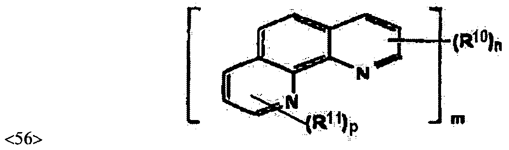
<57> [Formula 13]
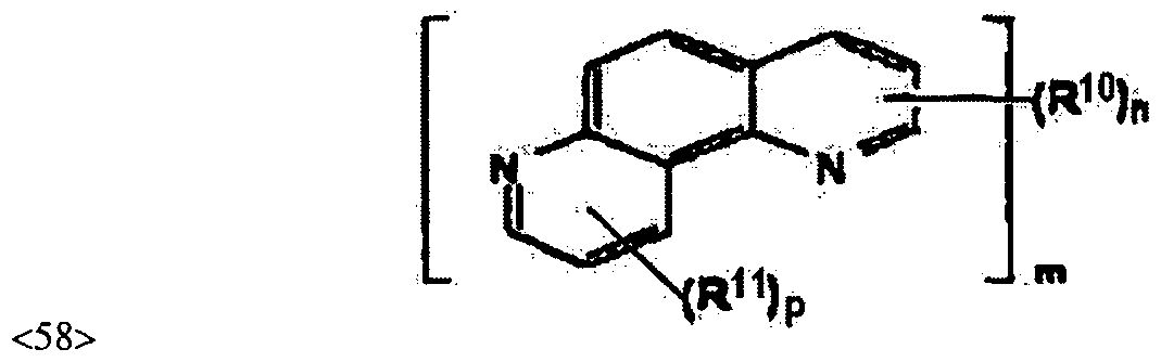


<64> when m is 1, R and R are each one selected from the group consisting
of hydrogen, an alkyl group such as methyl and ethyl, a cycloalkyl group such as cyclohexyl and a norbornyl , an aralkyl group such as benzyl group, an alkenyl group such as vinyl and allyl, a cycloalkenyl group such as cyclopentadienyl and cyclohexenyl , an alkoxy group such as methoxy, an alkylthio group in which an oxygen atom in ether bonding of an alkoxy group is substituted by a sulfur atom, an arylether group such as phenoxy, an arylthioether group in which an oxygen atom in ether bonding of an arylether group is substituted by a sulfur atom, an aryl group such as phenyl, naphthyl and biphenyl, a heterocyclic group such as furyl , thienyl, oxazolyl, pyridyl, quinolyl , carbazolyl , halogen, a cyano group, an aldehyde group, a carbonyl group, a carboxyl group, an ester group, a carbamoyl group, an amino group, a nitro group, a si IyI group such as trimethylsilyl , a siloxanyl group having silicon by ether bonding, and a ring structure that is formed in conjunction with an adjacent group!
10
<65> when m is 2 or more, R is a direct bond or a group having 2 or more
valence of the above-mentioned groups, and R is the same as the above- mentioned groups;
<66> the above substituent groups may be unsubstitueted or substituted, and the above substitutent groups are the same or different from each other when n or p is 2 or more.
<67> The compounds of Foumulae 12 to 15 are disclosed in Korean Patent Application Publication Nos. 2007-0052764 and 2007-0118711, the disclosures of which are incorporated herein by reference in its entirety.
<68> [Formula 16]
 <70> [Formula 17]

<72> [Formula 18]
 <74> [Formula 19]

<75>
la 8a Ib 10b
<76> In the Formulae 16 to 19, R to R and R to R are independently selected from the group consisting of a hydrogen atom, a substituted or unsubstituted aryl group having 5-60 nuclear atoms, a substituted or unsubstituted pyridyl group, a substituted or unsubstituted quinolyl group, a substituted or unsubstituted alkyl group having 1-50 carbon atoms, a substituted or unsubstituted cycloalkyl group having 3-50 carbon atoms, a substituted or unsubstituted aralkyl group having 6~50 nuclear atoms, a substituted or unsubstituted alkoxy group having 1-50 carbon atoms, a substituted or unsubstituted aryloxy group having 5-50 nuclear atoms, a substituted or unsubstituted arylthio group having 5-50 nuclear atoms, a substituted or unsubstituted alkoxycarbonyl group having 1-50 carbon atoms, an amino group substituted by a substituted or unsubstituted aryl group having 5-50 nuclear atoms, a halogen atom, a cyano group, a nitro group, a hydroxyl group and a carboxyl group, wherein the substituents are bonded each other to form an aromatic group; and L is a substituted or unsubstituted arylene group having 6-60 carbon atoms, a substituted or unsubstituted pyridynylene group, a substituted or unsubstituted quinolinylene group, or a substituted or unsubstituted fluorenylene group. The compounds of Formulae 16-19 are disclosed in Japanese Patent Application Publication No. 2007- 39405, the disclosures of which are incorporated herein by reference in its entirety. <77> [Formula 20]
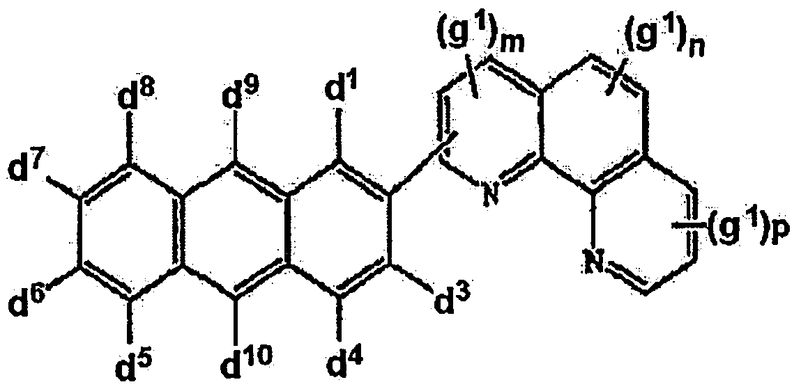

1 3 10 1
<80> In the Formulae 20 and 21, d , d to d and g are independently selected from the group consisting of a hydrogen atom and an aromatic or aliphatic hydrocarbon group, m and n are integers of 0 to 2, p is an integer of 0 to 3. The compounds of Formulae 20 and 21 are disclosed in U.S. Patent Application Publication No. 2007/0122656, the disclosures of which are incorporated herein by reference in its entirety.
<82> [Formula 22]

Ic 6c <84> In the Formula 22, R to R are independently selected from the group consisting of a hydrogen atom, a substituted or unsubstituted alkyl group, a substituted or unsubstituted aralkyl group, a substituted or unsubstituted aryl group, a substituted or unsubstituted heterocyclic group and a halogen atom, and Ar and Ar are independently selected from the following formulae:
<85>
 R 23
<86> wherein R17 to R23 are independently selected from the group consisting of a hydrogen atom, a substituted or unsubstituted alkyl group, a substituted or unsubstituted aralkyl group, a substituted or unsubstituted aryl group, a substituted or unsubstituted heterocyclic group and a halogen atom. The compound of Foumula 22 is disclosed in Japanese Patent Application Publication No. 2004-107263, the disclosures of which are incorporated herein by reference in its entirety.
R 23
<86> wherein R17 to R23 are independently selected from the group consisting of a hydrogen atom, a substituted or unsubstituted alkyl group, a substituted or unsubstituted aralkyl group, a substituted or unsubstituted aryl group, a substituted or unsubstituted heterocyclic group and a halogen atom. The compound of Foumula 22 is disclosed in Japanese Patent Application Publication No. 2004-107263, the disclosures of which are incorporated herein by reference in its entirety.
<87> In the present invention, when the organic material layer is formed by using the above-mentioned electron transporting material, at least one that is selected from the group consisting of metal halides, metal oxides and organic metal is doped as a doping material.
<88> Examples of the above metal halides include LiF, MgF2, NaF, KF, or the like. Examples of the above metal oxides include MgO, CaO, or the like. In the present invention, among the doping materials, it is more preferable to use metal halides, and it is even more preferable to use LiF.
<89> In the present invention, it is preferable that at least one selected from the group consisting of metal halides, metal oxides and organic metal be included in an amount in the range of 1 to 50% by weight based on the total weight of the materials of the organic material layer including the doping material .
<90> The organic material layer that includes the electron transporting material and the doping material may be formed by using a method that is known in the art. For example, a deposition method and a solvent process, for example, spin coating, dip coating, doctor blading, screen printing, inkjet printing, or thermal transfer method, may be used.
<9i> The organic light emitting device according to the present invention may be produced by using a typical production method and material and may have a structure known in the art, except that at least one organic material layer is formed by using the electron transporting material and the doping material .
<92> For example, the process of producing the organic light emitting device according to the present invention includes depositing metal, metal oxides having conductivity, or an alloy thereof on a substrate by using a PVD (physical vapor deposition) method such as sputtering or e-beam evaporation to form an anode, forming an organic material layer thereon, and forming a cathode thereon. In addition to the above-mentioned method, another method may be used. For example, the cathode, the organic material layer, and the anode may be sequentially deposited on the substrate to produce the organic light emitting device.
<93> The organic material layer may have a multi layered structure that includes the hole injecting layer, the hole transporting layer, the light emitting layer, the electron transporting layer, the electron injecting layer and the like. However, the structure of the organic material layer is not limited thereto, and a portion of the layers may be removed or additional layer may be provided. In the present invention, unlike the known technology, the electron injecting layer may not be formed to simplify the production process of the organic light emitting device and to produce the organic light emitting device having the excellent performance. Accordingly, the organic light emitting device according to the present invention may not include the electron injecting layer. That is, the organic material layer, including the electron transporting material and the doping material, may be in contact with any one electrode. However, the case of when the electron injecting layer is included is not excluded from the scope of the present invention. Therefore, an electron injecting layer can be positioned between any one electrode and the organic material layer including the electron transporting material and the doping material.
<94> The organic material layer may be produced by means of various types of polymer materials by using a deposition method as well as a solvent process such as spin coating, dip coating, doctor blading, screen printing, inkjet printing, heat transfer method or the like so that the organic material layer has a small number of layers.
<95> It is preferable that the anode material have a large work function so that a hole is desirably injected into the organic material layer. Specific examples of the anode material that is capable of being used in the present invention include, but are not limited to metal such as vanadium, chrome, copper, zinc, gold, nickel, and platinum, or an alloy thereof; metal oxides such as zinc oxides, indium oxides, indium tin oxides (ITO), and indium zinc oxides (IZO); metal/oxide composites such as ZnO^Al or Snθ2:Sb; and conductive polymers such as poly(3-methylthiophene), poly[3,4-(ethylene-l,2- dioxy)thiophene] (PEDT), polypyrrole, and polyaniline. In addition, in the case of when hexanitrile hexaazatriperylene that is represented by the following Formula is used as the material of the hole injecting layer, aluminum (Al), silver (Ag), calcium (Ca) or the like may be used. <96> (Formula)

<98> It is preferable that the cathode material have a small work function so that an electron is desirably injected into the organic material layer. Specific examples of the cathode material include, but are not limited to metal such as magnesium, calcium, sodium, potassium, titanium, indium, yttrium, lithium, gadolinium, aluminum, silver, tin, and lead, or an alloy thereof; and a multilayered material such as LiF/Al or LiO2Ml .
<99> The hole injecting material is a material that is capable of desirably receiving a hole from an anode at low voltage. It is preferable that the HOMO (highest occupied molecular orbital) level of the hole injecting material be located between the work function of the anode material and the HOMO level of its neighboring organic material layer. Specific examples of
the hole injecting material include, but are not limited to organic materials of metal porphyrin, oligothiophene, and arylamine series, organic materials of hexanitrile hexaazatriphenylene and quinacridone series, organic materials of perylene series, and conductive polymers of on anthraquinone, polyaniline, and polythiophene series.
<ioo> The hole transporting material is suitably a material having high hole mobility, which is capable of transferring holes from the anode or the hole injecting layer toward the light emitting layer. Specific examples of the hole transporting material include, but are not limited to organic materials of arylamine series, conductive polymers, and block copolymers having both conjugated portions and non-conjugated portions.
<ioi> The light emitting material is a material capable of emitting visible light by accepting and recombining holes from the hole transporting layer and electrons from the electron transporting layer, and preferably a material having high quantum efficiency for fluorescence and phosphorescence. Specific examples of the light emitting material include, but are not limited to 8-hydroxyquinoline aluminum complex (Alqs); compounds of carbazole series! dimerized styryl compounds! BAIq; 10-hydroxybenzoquinoline-metal compounds; compounds of benzoxazole, benzthiazole, and benzimidazole series; polymers of poly(p-phenylenevinylene) (PPV) series; spiro compounds; and compounds of polyfluorene and rubrene series.
<iO2> In addition, the organic material layer may comprise an n-type organic material layer in contact with one electrode of the first electrode and the second electrode and a p-type organic material layer forming an NP junction together with the n-type organic material layer wherein energy levels of the layers satisfy the following Expressions (1) and (2):
<i03> EnL - EFI < 4eV (1)

<i05> where EFI is a Fermi energy level of the electrode , EnL is an LUMO energy level of the n-type organic mater ial layer , and EpH i s an HOMO energy
level of the p-type organic material layer forming the NP junction together with the n-type organic material layer.
<iO6> When the energy difference between the LUMO energy level of the n-type organic material layer and the Fermi energy level of the electrode is more than 4 eV, an effect of a surface dipole or a gap state on an energy barrier for hole injection or hole extraction is reduced. Also, when the energy difference between the LUMO energy level of the n-type organic material layer and the HOMO energy level of the p-type organic material layer is more than approximately 1 eV, the NP junction of the p-type organic material layer and the n-type organic material layer is not easily formed and thus a driving voltage for hole injection or hole extraction increases.
<iO7> The compound represented by the following Formula 23 can be used as a material for the n-type organic material layer.
<iO8> [Formula 23]

Id 6d
<1 10> I Inn F Foorrmmuullaa 2233., eeaa<c ~hh oof R to R is selected from a group consisting of hydrogen, halogen atoms, nitrile (-CN), nitro (-NO2), sulfonyl (-SO2R), sulfoxide (-SOR), sulfonamide (-SO2NR), sulfonate (-SO3R), trifluoromethyl (- CF3), ester (-COOR), amide (-CONHR or -CONRR1), substituted or unsubstituted straight or branched chain C1-C12 alkoxy, substituted or unsubstituted straight or branched C1-C12 alkyl , substituted or unsubstituted aromatic or non-aromatic heterocyclic rings, substituted or unsubstituted aryl , substituted or unsubstituted mono- or di-arylamine, and substituted or unsubstituted aralkylamine, and each of R and R' are selected from a group
consisting of substituted or unsubstituted Ci-Ce0 alkyl, substituted or unsubstituted aryl , and substituted or unsubstituted 5-7 membered heterocyclic rings.
<111> Examples of the compound of Formula 23 may include compounds represented by the following Formulae 23-1 to 23-6.
<112> [Formula 23-1]

<U3> <114> [Formula 23-2]
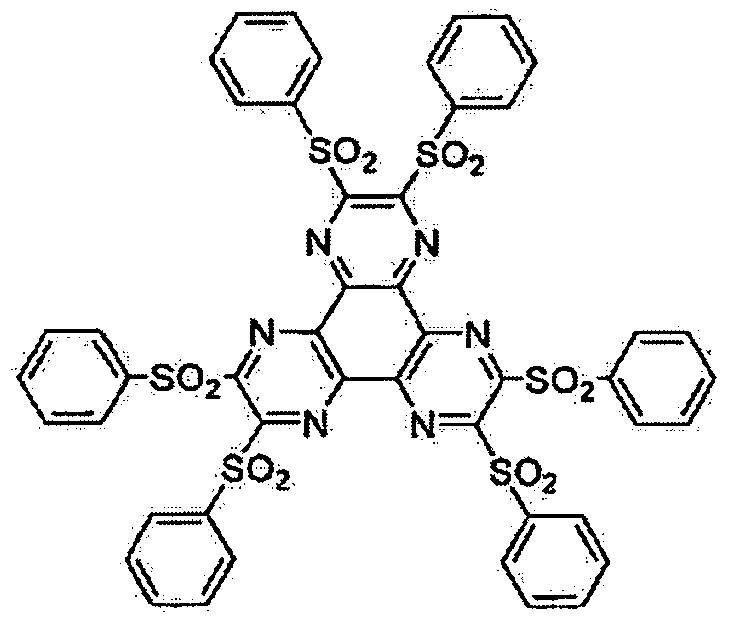
<115> <116> [Formula 23-3]

<117>
<118> [Formula 23-4]

<119> <120> [Formula 23-5]

<121> <122> [Formula 23-6]

<125> The p-type organic material layer, forming an NP junction together with the n-type organic material layer, may be a hole injection layer, a hole transport layer, or emitting layer.
<126> The organic light emitting device according to the present invention may be a top light emitting type, a bottom light emitting type, or a dual- sided light emitting type according to the type of material used. In addition, the organic light emitting device according to the present invention may have a negative structure in which the lower electrode is the cathode and the upper electrode is the anode or a positive structure in which the lower electrode is the anode and the upper electrode is the cathode. [Mode for Invention]
<i27> EXAMPLE
<i28> EXAMPLE 1
<129> LiF was doped on the electron transporting material of the following Formula in an amount of 20% on the Al thin film having the thickness of 700 A to form the layer having the thickness of 200 A. Subsequently, AIq3
(aluminum tris(8-hydroxyquinoline)) of the following Formula was deposited under a vacuum to form the light emitting layer having the thickness of 300 A, and NPB of the following Formula was deposited thereon under a vacuum to form the hole transporting layer having the thickness of 400 A. Subsequently, the HAT material of the following Formula was deposited thereon by heating under a vacuum to form the hole injecting layer having the thickness of 500 A. The IZO layer was formed thereon to have a thickness of 1750 A.
<130> [electron transporting material]

<132> [AIq3]


<135> <136> [HAT]
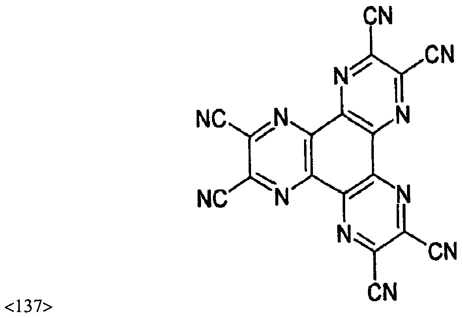
-7 -8
X lO to 2 X 10 torr during the deposit ion.
<139> Voltage was appl ied on the organic l ight emitt ing device that was
7
2 produced in Example 1 at the interval of 0.2 mA/cm to measure the voltage, the luminance, and the leakage current. The results are shown in FIGS. 1, 2, and 3. FIGS. 1, 2, and 3 are graphs that illustrate the current-voltage characteristic and the light emission characteristic of the organic light emitting device. In the above-mentioned graphs, when LiF was doped on the electron transporting material in an amount of 20%, if the electrons were not injected and transported, the normal rectifying property and light emission property were not obtained, but the voltage was high and the light emission property was reduced. However, as shown in FIGS. 1 and 2, the voltage was
2
3.6 V at 5 mA/cm , the luminance was 37.5 cd/A, and the leakage current characteristic shown in FIG. 3 was stable. Thus, the intrinsic device characteristics of the organic light emitting device were obtained.
<i4o> EXAMPLE 2
<i4i> LiF was doped on the electron transporting material of Example 1 in an amount of 0%, 10%, 20%, and 30% on the Al thin film having the thickness of 700 A to form the layer having the thickness of 1500 A. Subsequently, Al having the thickness of 700 A was deposited thereon. In respects to the four produced organic light emitting devices, the current density was measured according to bias voltage, and the results are shown in FIG.4.
<i42> FIG. 4 illustrates reverse direction and forward direction current- voltage characteristics of the organic light emitting devices produced in Example 2. In the case of when LiF was doped on the electron transporting material in an amount of 0%, it was difficult to inject the electrons. In the case of when LiF was doped on the electron transporting material in an amount of 10%, 20%, and 30%, the electron injection characteristic was significantly increased.
Claims
o
[CLAIMS] [Claim 1]
<144> An organic light emitting device comprising:
<i45> a first electrode;
<H6> a second electrode; and
<i47> at least one organic material layer that includes a light emitting layer disposed between the electrodes,
<i48> wherein at least one layer of the organic material layer includes an electron transporting material and at least one selected from the group consisting of metal halides, metal oxides and organic metal, and the electron transporting material is the compound having the functional group selected from the group consisting of an imidazole group, an oxazole group, a thiazole group, a quinoline group and a phenanthroline group.
[Claim 2]
<149> The organic light emitting device according to claim 1, wherein the organic material layer further includes a hole injecting layer, a hole transporting layer, or a hole injecting and transporting layer.
[Claim 3]
<15O> The organic light emitting device according to claim 1, wherein the organic material layer, including an electron transporting material and at least one selected from the group consisting of metal halides, metal oxides and organic metal, is in contact with any one of the first electrode and the second electrode. [Claim 4]
<i5i> The organic light emitting device according to claim 1, wherein the compound having the functional group that is selected from the group consisting of the imidazole group, the oxazole group, and the thiazole group is a compound of the following Formula 1 or 2: <152> [Formula 1]

1 4 <154> wherein R to R may be the same or different from each other, are each independently a hydrogen atom; a Ci to C30 alkyl group that is unsubstituted or substituted with one or more groups selected from the group consisting of a halogen atom, an amino group, a nitrile group, a nitro group, a Ci to C30 alkyl group, a C2 to C30 alkenyl group, a Ci to C30 alkoxy group, a C3 to C30 cycloalkyl group, a C3 to C30 heterocycloalkyl group, a Cs to C30 aryl group, and a C2 to C30 heteroaryl group; a C3 to C30 cycloalkyl group that is unsubstituted or substituted with one or more groups selected from the group consisting of a halogen atom, an amino group, a nitrile group, a nitro group, a Ci to C30 alkyl group, a C2 to C30 alkenyl group, a Ci to C30 alkoxy group, a C3 to C30 cycloalkyl group, a C3 to C30 heterocycloalkyl group, a Cs to C30 aryl group, and a C2 to C30 heteroaryl group; a Cs to C30 aryl group that is unsubstituted or substituted with one or more groups selected from the group consisting of a halogen atom, an amino group, a nitrile group, a nitro group, a Ci to C30 alkyl group, a C2 to
C30 alkenyl group, a Ci to C30 alkoxy group, a C3 to C30 cycloalkyl group, a C3 to C30 heterocycloalkyl group, a Cs to C30 aryl group, and a C2 to C30 heteroaryl group; or a C2 to C30 heteroaryl group that is unsubstituted or substituted with one or more groups selected from the group consisting of a halogen atom, an amino group, a nitrile group, a nitro group, a Ci to C30 alkyl group, a C2 to
C30 alkenyl group, a Ci to C30 alkoxy group, a C3 to C30 cycloalkyl group, a C3 to OvJ
C30 heterocycloalkyl group, a C5 to C30 aryl group, and a C2 to C30 heteroaryl group, and may form an aliphatic, aromatic, aliphatic hetero, or aromatic hetero condensation ring or a spiro bond in conjunction with a neighboring group; Ar is a hydrogen atom, a substituted or unsubstituted aromatic ring or
a substituted or unsubstituted aromatic hetero ring; X is 0, S, or NR , and R is hydrogen, a Ci to C7 aliphatic hydrocarbon, an aromatic ring or an aromatic hetero ring, <155> [Formula 2]

and R are each a hydrogen atom, a nitrile group (-CN), a nitro group (-NO2),
a Ci to C24 alkyl, a C5 to C20 aromatic ring or a hetero-atom substituted aromatic ring, a halogen, or an alkylene or an alkylene having a hetero-atom that can form a fused ring in conjunction with an adjacent ring; A and D may be connected to each other to form an aromatic or hetero aromatic ring; B is a linkage unit and substituted or unsubstituted alkylene or arylene that conjugately or unconjugately connects multiple hetero rings when n is 2 or more, and substituted or unsubstituted alkyl or aryl when n is 1; and n is an integer in the range of 1 to 8. [Claim 5]
<i58> The organic light emitting device according to claim 4, wherein the Formula 1 is represented by the following Formula 3: <i59> [Formula 3]

5 7
<i6i> wherein R to R are the same or different from each other, are each independently a hydrogen atom, a Ci to C20 aliphatic hydrocarbon, an aromatic ring, an aromatic hetero ring or an aliphatic or aromatic fused ring; Ar is a direct bond, an aromatic ring, an aromatic hetero ring, or an aliphatic or aromatic fused ring; and X is 0, S, or NR , R is a hydrogen atom, a Ci to C7
aliphatic hydrocarbon, an aromatic ring, or an aromatic hetero ring, with a
5 6 proviso that R and R can not simultaneously be hydrogen.
[Claim 6]
<162> The organic light emitting device according to claim 4, wherein the compound having the functional group that is selected from the group consisting of the imidazole group, the oxazole group, and the thiazole group is selected from compounds of the following Formulae:


<163>
[Claim 7]
<164> The organic light emitting device according to claim 1, wherein the compound having the quinoline group is selected from compounds of the following Formulae 5 to 11- <165> [Formula 5] 
<166> <167> [Formula 6]  <169> [Formula 7]
<170> <171> [Formula 8]  <173> [Formula 9]
<I 74> <175> [Formula 10]
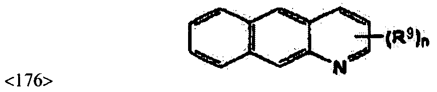
<177> [Formula 11]

<178> <179> wherein n is an integer in the range of 0 to 9, m is an integer in the range of 2 or more,
9
<180> R is one selected from the group consisting of hydrogen, an alkyl group, a cycloalkyl group, an aralkyl group, an alkenyl group, a cycloalkenyl group, an alkoxy group, an alkylthio group, an arylether group, an arylthioether group, an aryl group, a heterocyclic group, halogen, a cyano group, an aldehyde group, a carbonyl group, a carboxyl group, an ester group, a carbamoyl group, an amino group, a nitro group, a si IyI group, a siloxanyl group, and a ring structure that is formed in conjunction with an adjacent group; the above substituent groups may be unsubstitueted or substituted, and the above substitutent groups are the same or different from each other when n is 2 or more, and
9
<181> Y is a group having 2 or more valence of the above-mentioned R groups.
[Claim 8]
<182> The organic light emitting device according to claim 1, wherein the compound having the phenanthroline group is selected from the group consisting of compounds of the following Formulae 12 to 22: <183> [Formula 12]


10 11
<192> when m is 1, R and R are each one selected from the group consisting of hydrogen, an alkyl group, a cycloalkyl group, an aralkyl group, an alkenyl group, a cycloalkenyl group, an alkoxy group, an alkylthio group, an arylether group, an arylthioether group, an aryl group, a heterocyclic group, halogen, a cyano group, an aldehyde group, a carbonyl group, a carboxyl group, an ester group, a carbamoyl group, an amino group, a nitro group, a si IyI group, a siloxanyl group, and a ring structure that is formed in conjunction with an adjacent group;
10
<193> when m is 2 or more, R is a direct bond or a group having 2 or more
valence of the above-mentioned groups, and R is the same as the above- mentioned groups;
<194> the above substituent groups may be unsubstitueted or substituted, and the above substitutent groups are the same or different from each other when n or p is 2 or more,
<195> [Formula 16]


[Formula 21]

1 3 10 1
<204> wherein d , d to d and g are independently selected from the group consisting of a hydrogen atom and an aromatic or aliphatic hydrocarbon group, m and n are integers of 0 to 2, p is an integer of 0 to 3,
<209> [Formula 22]

Ic 6c <21 1> wherein R to R are independently selected from the group consisting of a hydrogen atom, a substituted or unsubstituted alkyl group, a substituted or unsubstituted aralkyl group, a substituted or unsubstituted aryl group, a substituted or unsubstituted heterocyclic group and a halogen atom, and Ar
2c and Ar are independently selected from the following formulae:

<2i3> wherein R17 to R23 are independently selected from the group consisting of a hydrogen atom, a substituted or unsubstituted alkyl group, a substituted or unsubstituted aralkyl group, a substituted or unsubstituted aryl group, a substituted or unsubstituted heterocyclic group and a halogen atom.
[Claim 9]
<2i4> The organic light emitting device according to claim 1, wherein the metal halides are selected from LiF, MgF2, NaF, and KF.
[Claim 10]
<2i5> The organic light emitting device according to claim 1, wherein the metal oxides are selected from MgO and CaO.
[Claim 11]
<2i6> The organic light emitting device according to claim 1, wherein the electron transporting material is a compound of the following Formula, and at least one selected from the group consisting of metal halides, metal oxides and organic metal is LiF:

[Claim 12]
<2i8> The organic light emitting device according to claim 1, wherein at least one selected from the group consisting of metal halides, metal oxides and organic metal is included in an amount in the range of 1 to 50% by weight based on a total weight of a material of the organic material layer including metal halides, metal oxides, inorganic metal, or organic metal.
[Claim 13]
<2i9> The organic light emitting device according to claim 1, wherein an electron injecting layer is positioned between any one of the first electrode and the second electrode and the organic material layer, including an electron transporting material and at least one selected from the group consisting of metal halides, metal oxides and organic metal.
[Claim 14]
<220> The organic light emitting device according to claim 1, wherein the organic material layer comprises an n-type organic material layer in contact with one electrode of the first electrode and the second electrode and a p- type organic material layer that forms an NP junction together with the n- type organic material layer, and energy levels of the layers satisfy the following Expressions (1) and (2):
<221> EnL - EFI < 4eV (1) 
<223> Wherein EFi is a Fermi energy level of the electrode, EnL is an LUMO energy level of the n-type organic material layer, and EPH is an HOMO energy level of the p-type organic material layer forming the NP junction together with the n-type organic material layer.
[Claim 15]
<224> A method of producing the organic light emitting device, comprising: <225> forming a first electrode; <226> forming at least one organic material layer including a light emitting layer on the first electrode; and
<227> forming a second electrode on the organic substance layer, <228> wherein at least one layer of the organic material layer is formed by doping at least one selected from the group consisting of metal halides, metal oxides and organic metal on an electron transporting material that is the compound having the functional group selected from the group consisting of an imidazole group, an oxazole group, a thiazole group, a quinoline group and a phenanthroline group.
Priority Applications (3)
| Application Number | Priority Date | Filing Date | Title |
|---|---|---|---|
| JP2010506078A JP2010526434A (en) | 2007-04-30 | 2008-04-30 | ORGANIC LIGHT EMITTING ELEMENT AND MANUFACTURING METHOD THEREOF |
| EP08753265.1A EP2139970B1 (en) | 2007-04-30 | 2008-04-30 | Organic light emitting device and method of producing the same |
| CN2008800141731A CN101675144B (en) | 2007-04-30 | 2008-04-30 | Organic light emitting device and method of producing the same |
Applications Claiming Priority (2)
| Application Number | Priority Date | Filing Date | Title |
|---|---|---|---|
| KR10-2007-0042085 | 2007-04-30 | ||
| KR20070042085 | 2007-04-30 |
Publications (2)
| Publication Number | Publication Date |
|---|---|
| WO2008133483A2 true WO2008133483A2 (en) | 2008-11-06 |
| WO2008133483A3 WO2008133483A3 (en) | 2008-12-18 |
Family
ID=39926211
Family Applications (1)
| Application Number | Title | Priority Date | Filing Date |
|---|---|---|---|
| PCT/KR2008/002465 Ceased WO2008133483A2 (en) | 2007-04-30 | 2008-04-30 | Organic light emitting device and method of producing the same |
Country Status (7)
| Country | Link |
|---|---|
| US (1) | US20080278072A1 (en) |
| EP (1) | EP2139970B1 (en) |
| JP (2) | JP2010526434A (en) |
| KR (1) | KR101025370B1 (en) |
| CN (1) | CN101675144B (en) |
| TW (1) | TWI500196B (en) |
| WO (1) | WO2008133483A2 (en) |
Cited By (5)
| Publication number | Priority date | Publication date | Assignee | Title |
|---|---|---|---|---|
| WO2010044607A1 (en) * | 2008-10-14 | 2010-04-22 | Cheil Industries Inc. | Benzimidazole compounds and organic photoelectric device with the same |
| JP2010225864A (en) * | 2009-03-24 | 2010-10-07 | Yamamoto Chem Inc | Organic transistor |
| JP2011046616A (en) * | 2009-08-25 | 2011-03-10 | Canon Inc | Heterocyclic compound and organic light-emitting device obtained by using the same |
| EP2299786A4 (en) * | 2008-05-16 | 2011-08-03 | Lg Chemical Ltd | STACKED ORGANIC ELECTROLUMINESCENT DIODE |
| WO2012005364A1 (en) * | 2010-07-09 | 2012-01-12 | 富士フイルム株式会社 | Organic electroluminescent element |
Families Citing this family (18)
| Publication number | Priority date | Publication date | Assignee | Title |
|---|---|---|---|---|
| WO2010058946A2 (en) * | 2008-11-18 | 2010-05-27 | 주식회사 엘지화학 | Novel chrysene derivatives and organic electrical device using the same |
| JP5868195B2 (en) * | 2011-04-14 | 2016-02-24 | キヤノン株式会社 | Novel spiro compound and organic light emitting device having the same |
| JP5858653B2 (en) * | 2011-06-08 | 2016-02-10 | キヤノン株式会社 | 6,12-Dinaphthylchrysene derivative and organic light-emitting device using the same |
| CN104488106B (en) * | 2012-05-25 | 2017-06-09 | 乐金显示有限公司 | Organic luminescent device and its manufacture method |
| US9246108B2 (en) * | 2012-12-28 | 2016-01-26 | Dow Global Technologies Llc | Quinoline-benzoxazole derived compounds for electronic films and devices |
| KR102137235B1 (en) * | 2013-02-07 | 2020-07-23 | 덕산네오룩스 주식회사 | Compound for organic electronic element, organic electronic element using the same, and an electronic device thereof |
| KR102077776B1 (en) * | 2013-05-22 | 2020-02-17 | 덕산네오룩스 주식회사 | An organic electronic element comprising a layer for improving light efficiency, and an electronic device comprising the same |
| CN103936781A (en) * | 2014-04-04 | 2014-07-23 | 常州大学 | Method for synthesizing phenanthridine silane derivative |
| JP6433852B2 (en) * | 2015-05-28 | 2018-12-05 | 株式会社東芝 | Compound, organic photoelectric conversion device, and solid-state imaging device |
| KR101980730B1 (en) * | 2015-11-17 | 2019-05-21 | 주식회사 엘지화학 | Nitrile based compound and organic light emitting device comprising the same |
| TWI619703B (en) * | 2016-05-18 | 2018-04-01 | 昱鐳光電科技股份有限公司 | Compound for organic electroluminescent device and organic electroluminescent device using the same |
| CN108735906B (en) * | 2017-04-20 | 2020-08-18 | Tcl科技集团股份有限公司 | Acrylate copolymer modified metal oxide, QLED and preparation method |
| KR102250385B1 (en) * | 2017-10-18 | 2021-05-11 | 주식회사 엘지화학 | Organic photodiode and organic image sensor comprising the same |
| KR102110833B1 (en) | 2018-12-06 | 2020-05-14 | 엘티소재주식회사 | Heterocyclic compound and organic light emitting device comprising the same |
| CN110845422A (en) * | 2019-11-28 | 2020-02-28 | 吉林奥来德光电材料股份有限公司 | An organic light-emitting compound, its synthesis method and organic electroluminescent device |
| US12016241B2 (en) * | 2020-02-13 | 2024-06-18 | Samsung Electronics Co., Ltd. | Quantum dot device, method of manufacturing the same, and electronic device |
| KR20240095561A (en) * | 2022-12-06 | 2024-06-26 | 삼성디스플레이 주식회사 | Electron transport layer comprising mixed composition, method of manufacturing light-emitting device, light-emitting device and electronic apparatus using the same |
| CN121925975A (en) * | 2023-10-13 | 2026-04-24 | 株式会社半导体能源研究所 | Light emitting device and light emitting apparatus |
Citations (6)
| Publication number | Priority date | Publication date | Assignee | Title |
|---|---|---|---|---|
| EP0949696A2 (en) | 1998-04-08 | 1999-10-13 | Idemitsu Kosan Company Limited | Organic electroluminescent device |
| US20030165715A1 (en) | 2002-01-18 | 2003-09-04 | Seok-Hee Yoon | New material for transporting electrons and organic electroluminescent display using the same |
| EP1722604A1 (en) | 2004-03-05 | 2006-11-15 | Idemitsu Kosan Co., Ltd. | Organic electroluminescence display device |
| EP1734038A1 (en) | 2004-04-07 | 2006-12-20 | Idemitsu Kosan Co., Ltd. | Nitrogenous heterocycle derivative and organic electroluminescent element employing the same |
| WO2007018004A1 (en) | 2005-08-05 | 2007-02-15 | Idemitsu Kosan Co., Ltd. | Nitrogenous heterocyclic derivative and organic electroluminescence device making use of the same |
| US20070069638A1 (en) | 2005-09-05 | 2007-03-29 | Idemitsu Kosan Co., Ltd. | Blue organic electroluminescent device |
Family Cites Families (17)
| Publication number | Priority date | Publication date | Assignee | Title |
|---|---|---|---|---|
| US5645948A (en) * | 1996-08-20 | 1997-07-08 | Eastman Kodak Company | Blue organic electroluminescent devices |
| US6800380B2 (en) * | 1998-06-23 | 2004-10-05 | Nessdisplay Co., Ltd. | Organometallic luminescent materials and organic electroluminescent device containing same |
| JP2000164359A (en) | 1998-11-25 | 2000-06-16 | Idemitsu Kosan Co Ltd | Organic electroluminescence device |
| US6420057B1 (en) * | 1999-07-05 | 2002-07-16 | Konica Corporation | Organic electroluminescent element |
| WO2001092437A1 (en) * | 2000-06-01 | 2001-12-06 | Nippon Steel Chemical Co., Ltd. | Organic electroluminescent element material and organic electroluminescent element |
| EP2365735B1 (en) * | 2000-11-24 | 2013-08-28 | Toray Industries Inc. | Luminescent element material and luminescent element comprising the same |
| US20050255331A1 (en) * | 2004-05-14 | 2005-11-17 | Krebs Robert R | Compound formable decorative laminate |
| US20060035109A1 (en) * | 2002-09-20 | 2006-02-16 | Idemitsu Kosan Co., Ltd. | Organic electroluminescent element |
| JP2004193011A (en) * | 2002-12-12 | 2004-07-08 | Fuji Photo Film Co Ltd | Organic electroluminescent element |
| US6849348B2 (en) * | 2002-12-31 | 2005-02-01 | Eastman Kodak Company | Complex fluorene-containing compounds |
| US6818329B1 (en) * | 2003-10-03 | 2004-11-16 | Eastman Kodak Company | Organic electroluminescent devices having a metal sub-layer within a hole-transporting region |
| CN100508238C (en) * | 2004-05-11 | 2009-07-01 | Lg化学株式会社 | Organic electronic device |
| KR100730132B1 (en) | 2005-05-30 | 2007-06-19 | 삼성에스디아이 주식회사 | Organic light emitting display device |
| JP4662306B2 (en) * | 2005-08-09 | 2011-03-30 | セイコーエプソン株式会社 | Electro-optical device, electronic equipment |
| US7553558B2 (en) * | 2005-11-30 | 2009-06-30 | Eastman Kodak Company | Electroluminescent device containing an anthracene derivative |
| JP2007294901A (en) * | 2006-03-31 | 2007-11-08 | Canon Inc | Organic light emitting device |
| KR100879477B1 (en) * | 2007-10-11 | 2009-01-20 | 삼성모바일디스플레이주식회사 | Organic light emitting device |
-
2008
- 2008-04-29 TW TW097115644A patent/TWI500196B/en active
- 2008-04-29 US US12/149,275 patent/US20080278072A1/en not_active Abandoned
- 2008-04-30 CN CN2008800141731A patent/CN101675144B/en active Active
- 2008-04-30 KR KR1020080040656A patent/KR101025370B1/en active Active
- 2008-04-30 JP JP2010506078A patent/JP2010526434A/en active Pending
- 2008-04-30 WO PCT/KR2008/002465 patent/WO2008133483A2/en not_active Ceased
- 2008-04-30 EP EP08753265.1A patent/EP2139970B1/en active Active
-
2013
- 2013-02-12 JP JP2013024226A patent/JP2013145889A/en active Pending
Patent Citations (6)
| Publication number | Priority date | Publication date | Assignee | Title |
|---|---|---|---|---|
| EP0949696A2 (en) | 1998-04-08 | 1999-10-13 | Idemitsu Kosan Company Limited | Organic electroluminescent device |
| US20030165715A1 (en) | 2002-01-18 | 2003-09-04 | Seok-Hee Yoon | New material for transporting electrons and organic electroluminescent display using the same |
| EP1722604A1 (en) | 2004-03-05 | 2006-11-15 | Idemitsu Kosan Co., Ltd. | Organic electroluminescence display device |
| EP1734038A1 (en) | 2004-04-07 | 2006-12-20 | Idemitsu Kosan Co., Ltd. | Nitrogenous heterocycle derivative and organic electroluminescent element employing the same |
| WO2007018004A1 (en) | 2005-08-05 | 2007-02-15 | Idemitsu Kosan Co., Ltd. | Nitrogenous heterocyclic derivative and organic electroluminescence device making use of the same |
| US20070069638A1 (en) | 2005-09-05 | 2007-03-29 | Idemitsu Kosan Co., Ltd. | Blue organic electroluminescent device |
Non-Patent Citations (1)
| Title |
|---|
| See also references of EP2139970A4 |
Cited By (10)
| Publication number | Priority date | Publication date | Assignee | Title |
|---|---|---|---|---|
| EP2299786A4 (en) * | 2008-05-16 | 2011-08-03 | Lg Chemical Ltd | STACKED ORGANIC ELECTROLUMINESCENT DIODE |
| US8637854B2 (en) | 2008-05-16 | 2014-01-28 | Lg Chem, Ltd. | Stacked organic light emitting diode |
| WO2010044607A1 (en) * | 2008-10-14 | 2010-04-22 | Cheil Industries Inc. | Benzimidazole compounds and organic photoelectric device with the same |
| US9530970B2 (en) | 2008-10-14 | 2016-12-27 | Cheil Industries, Inc. | Benzimidazole compound, organic photoelectric device including the same, and display element including the same |
| JP2010225864A (en) * | 2009-03-24 | 2010-10-07 | Yamamoto Chem Inc | Organic transistor |
| JP2011046616A (en) * | 2009-08-25 | 2011-03-10 | Canon Inc | Heterocyclic compound and organic light-emitting device obtained by using the same |
| US8877354B2 (en) | 2009-08-25 | 2014-11-04 | Canon Kabushiki Kaisha | Heterocyclic compound and organic light-emitting device using the same |
| WO2012005364A1 (en) * | 2010-07-09 | 2012-01-12 | 富士フイルム株式会社 | Organic electroluminescent element |
| JP2012019176A (en) * | 2010-07-09 | 2012-01-26 | Fujifilm Corp | Organic electroluminescent element |
| KR20130097715A (en) | 2010-07-09 | 2013-09-03 | 유디씨 아일랜드 리미티드 | Organic electroluminescent element |
Also Published As
| Publication number | Publication date |
|---|---|
| EP2139970A2 (en) | 2010-01-06 |
| US20080278072A1 (en) | 2008-11-13 |
| JP2010526434A (en) | 2010-07-29 |
| KR20080097153A (en) | 2008-11-04 |
| CN101675144B (en) | 2013-06-26 |
| TWI500196B (en) | 2015-09-11 |
| JP2013145889A (en) | 2013-07-25 |
| KR101025370B1 (en) | 2011-03-28 |
| WO2008133483A3 (en) | 2008-12-18 |
| TW200905942A (en) | 2009-02-01 |
| CN101675144A (en) | 2010-03-17 |
| EP2139970A4 (en) | 2011-08-03 |
| EP2139970B1 (en) | 2014-09-24 |
Similar Documents
| Publication | Publication Date | Title |
|---|---|---|
| CN101675144B (en) | Organic light emitting device and method of producing the same | |
| KR101069520B1 (en) | Organic light emitting device and its manufacturing method | |
| KR102055479B1 (en) | Organic Electroluminescent Element | |
| KR100823443B1 (en) | High efficiency organic light emitting device and its manufacturing method | |
| US10522762B2 (en) | Organic light emitting diode including an organic layer having a compound with at least a nitrogen-containing heteroring group | |
| CN102317406B (en) | Heterocyclic compounds and their applications in electronic and optoelectronic structural elements | |
| CN104335379B (en) | Organic electroluminescence device, the display comprising this organic electroluminescence device and luminaire | |
| US20090015150A1 (en) | Organic light emitting device and method for manufacturing the same | |
| US11239431B2 (en) | Organic electronic device, organic semiconducting material and a borane compound | |
| US10916724B2 (en) | Organic light emitting device | |
| KR102218349B1 (en) | Organic light emitting device | |
| KR101539842B1 (en) | Organic light emitting device | |
| US20230006161A1 (en) | Organic light-emitting device | |
| KR20210155532A (en) | Organic light emitting diode | |
| KR101849825B1 (en) | Organic light emitting diode | |
| TW201341446A (en) | Organic electroluminescent element | |
| KR20200072679A (en) | organic light-emitting diode with low operating voltage and High efficiency | |
| KR101896143B1 (en) | Organic light emitting diode | |
| KR20160132615A (en) | Stacked organic light emitting device |
Legal Events
| Date | Code | Title | Description |
|---|---|---|---|
| WWE | Wipo information: entry into national phase |
Ref document number: 200880014173.1 Country of ref document: CN |
|
| 121 | Ep: the epo has been informed by wipo that ep was designated in this application |
Ref document number: 08753265 Country of ref document: EP Kind code of ref document: A2 |
|
| WWE | Wipo information: entry into national phase |
Ref document number: 2008753265 Country of ref document: EP |
|
| WWE | Wipo information: entry into national phase |
Ref document number: 2010506078 Country of ref document: JP |
|
| NENP | Non-entry into the national phase |
Ref country code: DE |