WO2009093366A1 - 金属化合物、これを含有してなる化学気相成長用原料及び金属含有薄膜の製造方法 - Google Patents
金属化合物、これを含有してなる化学気相成長用原料及び金属含有薄膜の製造方法 Download PDFInfo
- Publication number
- WO2009093366A1 WO2009093366A1 PCT/JP2008/069121 JP2008069121W WO2009093366A1 WO 2009093366 A1 WO2009093366 A1 WO 2009093366A1 JP 2008069121 W JP2008069121 W JP 2008069121W WO 2009093366 A1 WO2009093366 A1 WO 2009093366A1
- Authority
- WO
- WIPO (PCT)
- Prior art keywords
- thin film
- chemical vapor
- vapor deposition
- metal
- metal compound
- Prior art date
- Legal status (The legal status is an assumption and is not a legal conclusion. Google has not performed a legal analysis and makes no representation as to the accuracy of the status listed.)
- Ceased
Links
Images

Classifications
-
- C—CHEMISTRY; METALLURGY
- C23—COATING METALLIC MATERIAL; COATING MATERIAL WITH METALLIC MATERIAL; CHEMICAL SURFACE TREATMENT; DIFFUSION TREATMENT OF METALLIC MATERIAL; COATING BY VACUUM EVAPORATION, BY SPUTTERING, BY ION IMPLANTATION OR BY CHEMICAL VAPOUR DEPOSITION, IN GENERAL; INHIBITING CORROSION OF METALLIC MATERIAL OR INCRUSTATION IN GENERAL
- C23C—COATING METALLIC MATERIAL; COATING MATERIAL WITH METALLIC MATERIAL; SURFACE TREATMENT OF METALLIC MATERIAL BY DIFFUSION INTO THE SURFACE, BY CHEMICAL CONVERSION OR SUBSTITUTION; COATING BY VACUUM EVAPORATION, BY SPUTTERING, BY ION IMPLANTATION OR BY CHEMICAL VAPOUR DEPOSITION, IN GENERAL
- C23C16/00—Chemical coating by decomposition of gaseous compounds, without leaving reaction products of surface material in the coating, i.e. chemical vapour deposition [CVD] processes
- C23C16/44—Chemical coating by decomposition of gaseous compounds, without leaving reaction products of surface material in the coating, i.e. chemical vapour deposition [CVD] processes characterised by the method of coating
- C23C16/455—Chemical coating by decomposition of gaseous compounds, without leaving reaction products of surface material in the coating, i.e. chemical vapour deposition [CVD] processes characterised by the method of coating characterised by the method used for introducing gases into reaction chamber or for modifying gas flows in reaction chamber
- C23C16/45523—Pulsed gas flow or change of composition over time
- C23C16/45525—Atomic layer deposition [ALD]
- C23C16/45553—Atomic layer deposition [ALD] characterized by the use of precursors specially adapted for ALD
-
- C—CHEMISTRY; METALLURGY
- C07—ORGANIC CHEMISTRY
- C07F—ACYCLIC, CARBOCYCLIC OR HETEROCYCLIC COMPOUNDS CONTAINING ELEMENTS OTHER THAN CARBON, HYDROGEN, HALOGEN, OXYGEN, NITROGEN, SULFUR, SELENIUM OR TELLURIUM
- C07F7/00—Compounds containing elements of Groups 4 or 14 of the Periodic Table
- C07F7/003—Compounds containing elements of Groups 4 or 14 of the Periodic Table without C-Metal linkages
-
- C—CHEMISTRY; METALLURGY
- C23—COATING METALLIC MATERIAL; COATING MATERIAL WITH METALLIC MATERIAL; CHEMICAL SURFACE TREATMENT; DIFFUSION TREATMENT OF METALLIC MATERIAL; COATING BY VACUUM EVAPORATION, BY SPUTTERING, BY ION IMPLANTATION OR BY CHEMICAL VAPOUR DEPOSITION, IN GENERAL; INHIBITING CORROSION OF METALLIC MATERIAL OR INCRUSTATION IN GENERAL
- C23C—COATING METALLIC MATERIAL; COATING MATERIAL WITH METALLIC MATERIAL; SURFACE TREATMENT OF METALLIC MATERIAL BY DIFFUSION INTO THE SURFACE, BY CHEMICAL CONVERSION OR SUBSTITUTION; COATING BY VACUUM EVAPORATION, BY SPUTTERING, BY ION IMPLANTATION OR BY CHEMICAL VAPOUR DEPOSITION, IN GENERAL
- C23C16/00—Chemical coating by decomposition of gaseous compounds, without leaving reaction products of surface material in the coating, i.e. chemical vapour deposition [CVD] processes
- C23C16/22—Chemical coating by decomposition of gaseous compounds, without leaving reaction products of surface material in the coating, i.e. chemical vapour deposition [CVD] processes characterised by the deposition of inorganic material, other than metallic material
- C23C16/30—Deposition of compounds, mixtures or solid solutions, e.g. borides, carbides, nitrides
- C23C16/308—Oxynitrides
-
- C—CHEMISTRY; METALLURGY
- C23—COATING METALLIC MATERIAL; COATING MATERIAL WITH METALLIC MATERIAL; CHEMICAL SURFACE TREATMENT; DIFFUSION TREATMENT OF METALLIC MATERIAL; COATING BY VACUUM EVAPORATION, BY SPUTTERING, BY ION IMPLANTATION OR BY CHEMICAL VAPOUR DEPOSITION, IN GENERAL; INHIBITING CORROSION OF METALLIC MATERIAL OR INCRUSTATION IN GENERAL
- C23C—COATING METALLIC MATERIAL; COATING MATERIAL WITH METALLIC MATERIAL; SURFACE TREATMENT OF METALLIC MATERIAL BY DIFFUSION INTO THE SURFACE, BY CHEMICAL CONVERSION OR SUBSTITUTION; COATING BY VACUUM EVAPORATION, BY SPUTTERING, BY ION IMPLANTATION OR BY CHEMICAL VAPOUR DEPOSITION, IN GENERAL
- C23C16/00—Chemical coating by decomposition of gaseous compounds, without leaving reaction products of surface material in the coating, i.e. chemical vapour deposition [CVD] processes
- C23C16/22—Chemical coating by decomposition of gaseous compounds, without leaving reaction products of surface material in the coating, i.e. chemical vapour deposition [CVD] processes characterised by the deposition of inorganic material, other than metallic material
- C23C16/30—Deposition of compounds, mixtures or solid solutions, e.g. borides, carbides, nitrides
- C23C16/34—Nitrides
-
- C—CHEMISTRY; METALLURGY
- C23—COATING METALLIC MATERIAL; COATING MATERIAL WITH METALLIC MATERIAL; CHEMICAL SURFACE TREATMENT; DIFFUSION TREATMENT OF METALLIC MATERIAL; COATING BY VACUUM EVAPORATION, BY SPUTTERING, BY ION IMPLANTATION OR BY CHEMICAL VAPOUR DEPOSITION, IN GENERAL; INHIBITING CORROSION OF METALLIC MATERIAL OR INCRUSTATION IN GENERAL
- C23C—COATING METALLIC MATERIAL; COATING MATERIAL WITH METALLIC MATERIAL; SURFACE TREATMENT OF METALLIC MATERIAL BY DIFFUSION INTO THE SURFACE, BY CHEMICAL CONVERSION OR SUBSTITUTION; COATING BY VACUUM EVAPORATION, BY SPUTTERING, BY ION IMPLANTATION OR BY CHEMICAL VAPOUR DEPOSITION, IN GENERAL
- C23C16/00—Chemical coating by decomposition of gaseous compounds, without leaving reaction products of surface material in the coating, i.e. chemical vapour deposition [CVD] processes
- C23C16/22—Chemical coating by decomposition of gaseous compounds, without leaving reaction products of surface material in the coating, i.e. chemical vapour deposition [CVD] processes characterised by the deposition of inorganic material, other than metallic material
- C23C16/30—Deposition of compounds, mixtures or solid solutions, e.g. borides, carbides, nitrides
- C23C16/40—Oxides
Definitions
- the present invention relates to a novel metal compound having a specific structure, a raw material for chemical vapor deposition containing the same, and a method for producing a metal-containing thin film using the raw material.
- Thin films containing titanium, zirconium, or hafnium are used for electronic components such as high-dielectric capacitors, ferroelectric capacitors, gate films, barrier films, and gate insulating films, and optical components such as optical waveguides, optical switches, and optical amplifiers. It is used as an optical member for communication devices.
- Examples of the method for producing the thin film include a MOD method such as a coating pyrolysis method and a sol-gel method, a chemical vapor deposition method such as a CVD method and an ALD method, etc., and excellent composition controllability and step coverage. Since it has many advantages such as being suitable for mass production and being capable of hybrid integration, the chemical vapor deposition method using vaporized precursors such as CVD and ALD is the optimum manufacturing process. Metal precursors using organic ligands are used as precursors for CVD and ALD methods.
- Metal nitride thin films whose metal atoms are titanium, zirconium or hafnium are used as coating layers for improving hardness and strength of cutting tools, gate thin films for semiconductor devices, and barrier films. Many techniques for manufacturing by the growth method have been reported.
- Patent Document 1 discloses a method for producing a metal nitride and / or metal carbide thin film using a halide of titanium, zirconium, hafnium, vanadium, niobium or tantalum
- Patent Document 2 discloses titanium tetrachloride. And a method for producing a titanium nitride thin film by a CVD method using ammonia gas.
- Patent Documents 2 to 5 disclose a method for producing a Group 4 metal-containing thin film using a dialkylamino metal compound having an organic amine as a ligand as a precursor of titanium, zirconium or hafnium. A metal compound using ethylmethylamine as a child is disclosed.
- a method using a chloride typified by titanium tetrachloride requires a temperature of at least about 500 ° C. to form a thin film, and is not suitable for use in manufacturing a semiconductor element such as a gate film.
- an organic amide-based metal compound having an organic amine as a ligand can produce a metal nitride thin film at a low temperature, but it is expected because the thin film obtained using this has a large amount of residual carbon. It is difficult to realize electrical characteristics, and application as a gate film, a barrier film, and an electrode film that are particularly required to be conductive is difficult.
- Patent Document 6 discloses Ti (N (CH 3 ) 2 ) 3 X, Ti (N (CH 3 ) 2 ) 2 X 2 , Ti (N (C 2 H 5 ) 2 ) 3 X, Ti (N (C A method for producing a titanium nitride thin film by a CVD method using 2 H 5 ) 2 ) 2 X 2 (X is a halogen atom) is disclosed. There is a disclosure that these titanium compounds have high thermal decomposability and can be suitably used as a gate thin film material. However, Ti (N (CH 3 ) 2 ) 3 Cl and Ti (N (CH 3 ) 2 ) 3 Cl, which are typically used in Patent Document 6, are solid and have a melting point when used as a CVD material.
- the problem to be solved by the present invention is to provide a metal compound that gives a good metal-containing thin film with little residual carbon and gives a stable process for film formation speed and thin film composition control.
- the chemical vapor deposition raw material in the present invention represents both a CVD raw material and an ALD raw material unless otherwise specified.
- the present invention provides a metal compound represented by the following general formula (1).
- M represents titanium, zirconium or hafnium
- X represents a halogen atom
- m 1 or 2.
- the present invention also provides a raw material for chemical vapor deposition containing the above metal compound.
- the present invention also provides a method for producing a metal-containing thin film by chemical vapor deposition using the above chemical vapor deposition raw material.
- the metal compound of the present invention is a novel compound represented by the above general formula (1).
- examples of the halogen atom represented by X include fluorine, chlorine, bromine and iodine.
- chlorine is preferred because the raw material is inexpensive and highly volatile.
- the thermal decomposition temperature is lower than that when 1.
- a material having a large difference between the volatilization temperature (vapor temperature) and the thin film deposition temperature (reaction temperature) can be used because it can provide a wide process margin. Therefore, the larger process margin may be selected for m.
- M is a titanium atom
- metal compound of the present invention include the following compound No. 1 to 24.
- the metal compound of the present invention is not particularly limited by the production method, and is produced by applying a known reaction.
- the production method for example, MX 4 (M and X are the same as in the above general formula (1)) and a method of reacting with an amount of ethyl methylamine necessary to give the desired m, MX 4 and the desired And a method based on a reaction with an amount of M (NEtMe) 4 necessary to give m.
- a method is preferred in which alkyl lithium is used as a reactant and MX 4 is reacted with ethyl 4 via aminomethylamino lithium as a reactive intermediate.
- MX 4 and M (NEtMe) 4 are mixed and stirred at a temperature necessary for the reaction.
- the production of the metal compound of the present invention is performed in an environment in which reactive active species such as moisture, oxygen and carbon dioxide are excluded from the system as much as possible.
- the raw material for chemical vapor deposition of the present invention is a thin film precursor made of the metal compound represented by the general formula (1), and the form thereof is a transportation supply method of the chemical vapor deposition method used, etc. This method is appropriately selected.
- the chemical vapor deposition raw material is vaporized by heating and / or depressurizing in the raw material container, and together with a carrier gas such as argon, nitrogen, helium, etc. used as needed, to the deposition reaction section.
- a carrier gas such as argon, nitrogen, helium, etc. used as needed.
- the chemical vapor deposition raw material is transported to the vaporization chamber in a liquid or solution state, vaporized by heating and / or decompressing in the vaporization chamber, and then transported to the deposition reaction section
- a carrier gas such as argon, nitrogen, helium, etc.
- the metal compound itself represented by the general formula (1) is a raw material for chemical vapor deposition
- the metal compound itself represented by the general formula (1) or A solution obtained by dissolving the metal compound in an organic solvent serves as a raw material for chemical vapor deposition.
- a method for vaporizing and supplying chemical vapor deposition materials independently for each component (hereinafter referred to as a single source method).
- a method of vaporizing and supplying a mixed raw material in which a multi-component raw material is mixed in advance with a desired composition (hereinafter sometimes referred to as a cocktail sauce method).
- a cocktail sauce method a mixture of only the metal compound represented by the general formula (1) or a mixed solution obtained by adding an organic solvent to these mixtures, the metal compound represented by the general formula (1) and other precursors Or a mixed solution obtained by adding an organic solvent to these mixtures is a raw material for chemical vapor deposition.
- the organic solvent used for the chemical vapor deposition raw material is not particularly limited, and a known general organic solvent that does not react with the metal compound of the present invention can be used.
- the organic solvent include acetates such as ethyl acetate, butyl acetate and methoxyethyl acetate; ethers such as tetrahydrofuran, tetrahydropyran, morpholine, ethylene glycol dimethyl ether, diethylene glycol dimethyl ether, triethylene glycol dimethyl ether, dibutyl ether and dioxane.
- Ketones such as methyl butyl ketone, methyl isobutyl ketone, ethyl butyl ketone, dipropyl ketone, diisobutyl ketone, methyl amyl ketone, cyclohexanone and methylcyclohexanone; hexane, cyclohexane, methylcyclohexane, dimethylcyclohexane, ethylcyclohexane, heptane, octane, Hydrocarbons such as toluene and xylene; acetonitrile, 1-cyanopropane, 1-silane Cyanogens such as nobutane, 1-cyanohexane, cyanocyclohexane, cyanobenzene, 1,3-dicyanopropane, 1,4-dicyanobutane, 1,6-dicyanohexane, 1,4-dicyanocyclohexan
- the total amount of the metal compound components of the present invention in the organic solvent is 0.01 to 2.0 mol / liter, particularly 0.05 to 1.0 mol / liter. It is preferable to do this.
- Examples of the other precursor include one or more selected from the group consisting of compounds used as organic ligands such as alcohol compounds, glycol compounds, ⁇ -diketone compounds, cyclopentadiene compounds, and organic amine compounds. , Compounds with silicon, boron, phosphorus or metal.
- metal species include Group 1 elements such as lithium, sodium, potassium, rubidium, and cesium, Group 2 elements such as beryllium, magnesium, calcium, strontium, and barium, scandium, yttrium, and lanthanoid elements (lanthanum, cerium, praseodymium, neodymium, Promethium, samarium, europium, gadolinium, terbium, dysprosium, holmium, erbium, thulium, ytterbium, lutetium), group 3 elements such as actinoid elements, group 4 elements such as titanium, zirconium, hafnium, group 5 of vanadium, niobium, tantalum Element, chromium, molybdenum, tungsten group 6 element, manganese, technetium, rhenium group 7 element, iron, ruthenium, osmium group 8 element, cobalt, rhodium, iridium Group 9 elements
- Examples of the alcohol compound used as the organic ligand include alkyl alcohols such as methanol, ethanol, propanol, isopropanol, butanol, 2-butanol, isobutanol, tertiary butanol, amyl alcohol, isoamyl alcohol, and tertiary amyl alcohol.
- alkyl alcohols such as methanol, ethanol, propanol, isopropanol, butanol, 2-butanol, isobutanol, tertiary butanol, amyl alcohol, isoamyl alcohol, and tertiary amyl alcohol.
- glycol compound used as the organic ligand examples include 1,2-ethanediol, 1,2-propanediol, 1,3-propanediol, 2,4-hexanediol, 2,2-dimethyl-1, 3-propanediol, 2,2-diethyl-1,3-propanediol, 1,3-butanediol, 2,4-butanediol, 2,2-diethyl-1,3-butanediol, 2-ethyl-2 -Butyl-1,3-propanediol, 2,4-pentanediol, 2-methyl-1,3-propanediol, 2-methyl-2,4-pentanediol, 2,4-hexanediol, 2,4- Examples thereof include dimethyl-2,4-pentanediol.
- Examples of the ⁇ -diketone compound used as the organic ligand include acetylacetone, hexane-2,4-dione, 5-methylhexane-2,4-dione, heptane-2,4-dione, 2-methylheptane- 3,5-dione, 5-methylheptane-2,4-dione, 6-methylheptane-2,4-dione, 2,2-dimethylheptane-3,5-dione, 2,6-dimethylheptane-3, 5-dione, 2,2,6-trimethylheptane-3,5-dione, 2,2,6,6-tetramethylheptane-3,5-dione, octane-2,4-dione, 2,2,6 -Trimethyloctane-3,5-dione, 2,6-dimethyloctane-3,5-dione, 2,9-dimethylnonane-4,6-dione 2-methyl-6-e
- cyclopentadiene compound used as the organic ligand examples include cyclopentadiene, methylcyclopentadiene, ethylcyclopentadiene, propylcyclopentadiene, isopropylcyclopentadiene, butylcyclopentadiene, second butylcyclopentadiene, isobutylcyclopentadiene, third Examples include butylcyclopentadiene, dimethylcyclopentadiene, tetramethylcyclopentadiene, and pentamethylcyclopentadiene.
- organic amine compound used as the organic ligand examples include methylamine, ethylamine, propylamine, isopropylamine, butylamine, tertiary butylamine, secondary butylamine, isobutylamine, dimethylamine, diethylamine, dipropylamine, and diisopropylamine. , Ethylmethylamine, propylmethylamine, isopropylmethylamine and the like.
- the other precursor in the multi-component chemical vapor deposition method is preferably a compound similar to the metal compound of the present invention in reaction or decomposition behavior changing to a thin film composition.
- a compound reactive to the formed molecular layer (the metal compound layer of the present invention or an intermediate layer formed by reaction thereof) is preferable.
- the cocktail sauce method in addition to the behavior of the change to the thin film composition being similar, a method that does not cause alteration due to a chemical reaction during mixing is preferable.
- the chemical vapor deposition raw material of the present invention may contain a nucleophilic reagent as needed to impart stability of the metal compound of the present invention and other precursors.
- the nucleophile include ethylene glycol ethers such as glyme, diglyme, triglyme and tetraglyme, 18-crown-6, dicyclohexyl-18-crown-6, 24-crown-8, dicyclohexyl-24-crown-8, Crown ethers such as dibenzo-24-crown-8, ethylenediamine, N, N′-tetramethylethylenediamine, diethylenetriamine, triethylenetetramine, tetraethylenepentamine, pentaethylenehexamine, 1,1,4,7,7-penta Polyamines such as methyldiethylenetriamine, 1,1,4,7,10,10-hexamethyltriethylenetetramine and triethoxytriethyleneamine, cyclic polyamines such as cyclam and cyclen,
- the raw material for chemical vapor deposition of the present invention contains as little impurities metal elements as possible other than the components constituting it, impurity halogens such as chlorine, and impurity organics as much as possible.
- the impurity metal element content is preferably 100 ppb or less and more preferably 10 ppb or less for each element.
- the total amount is preferably 1 ppm or less, and more preferably 100 ppb or less.
- metal oxides, complex metal oxides with silicon, nitrides, nitride oxides with silicon, etc. are used as LSI gate insulating films, gate films, and barrier layers, the electrical characteristics of the resulting thin film are affected.
- the impurity halogen content is preferably 100 ppm or less, more preferably 10 ppm or less, and still more preferably 1 ppm or less.
- the total amount of impurity organic components is preferably 500 ppm or less, more preferably 50 ppm or less, and still more preferably 10 ppm or less.
- metal compounds, organic solvents, and nucleophilic reagents are used for reducing their respective moisture. It is better to remove moisture as much as possible.
- the water content of each of the metal compound, organic solvent and nucleophilic reagent is preferably 10 ppm or less, more preferably 1 ppm or less.
- the chemical vapor deposition material of the present invention is larger than 0.3 ⁇ m in the particle measurement by the light scattering submerged particle detector in the liquid phase in order to reduce or prevent the particle contamination of the thin film to be produced.
- the number of particles is preferably 100 or less in 1 ml of liquid phase, more preferably 1000 or less in 1 ml of liquid phase, and the number of particles greater than 0.2 ⁇ m. Is more preferably 100 or less in 1 ml of the liquid phase.
- the method for producing a thin film of the present invention includes introducing a vapor obtained by vaporizing the metal compound of the present invention and other precursors used as necessary, and a reactive gas used as necessary, onto a substrate,
- the chemical vapor deposition method is used in which a precursor is decomposed and / or reacted on a substrate to grow and deposit a thin film on the substrate.
- Examples of the reactive gas used as needed include, for example, oxygen, ozone, nitrogen dioxide, nitrogen monoxide, water vapor, hydrogen peroxide, formic acid, acetic acid, which are oxidizing gases for producing oxides.
- Acetic anhydride and the like can be mentioned, hydrogen as the reducing agent, and those producing the nitride include organic amine compounds such as monoalkylamine, dialkylamine, trialkylamine, alkylenediamine, hydrazine, Ammonia, nitrogen and the like can be mentioned.
- examples of the transportation and supply method include the gas transportation method, the liquid transportation method, the single source method, and the cocktail sauce method.
- the source gas, or the thermal CVD in which the source gas and the reactive gas are reacted only by heat to deposit a thin film examples include optical plasma CVD using heat, light, and plasma, and ALD (Atomic Layer Deposition) in which the deposition reaction of CVD is divided into elementary processes and deposition is performed stepwise at the molecular level.
- examples of the manufacturing conditions include reaction temperature (substrate temperature), reaction pressure, and deposition rate.
- the reaction temperature is preferably 150 ° C. or higher, which is the temperature at which the metal compound of the present invention sufficiently reacts, and more preferably 250 ° C. to 450 ° C.
- the reaction pressure is preferably from atmospheric pressure to 10 Pa in the case of thermal CVD or photo CVD, and is preferably from 10 Pa to 2000 Pa in the case of using plasma.
- the deposition rate can be controlled by the raw material supply conditions (vaporization temperature, vaporization pressure), reaction temperature, and reaction pressure. When the deposition rate is large, the properties of the obtained thin film may be deteriorated. When the deposition rate is small, productivity may be problematic.
- the deposition rate is preferably 0.5 to 5000 nm / min, and more preferably 1 to 1000 nm / min.
- the number of cycles is controlled so as to obtain a desired film thickness.
- the thickness of the thin film formed from the raw material for chemical vapor deposition of the present invention is appropriately selected depending on the application, but is preferably selected from 0.1 to 1000 nm.
- the metal compound of the present invention gives a metal nitride having a small impurity content such as residual carbon, it is preferably used for the production of a metal nitride-based thin film.
- a preferred method for producing a metal nitride thin film using the chemical vapor deposition material of the present invention is ALD.
- ALD the raw material, the reactive gas used as needed, and other precursors used as needed are alternately supplied to the deposition part, and this is used as one cycle to step the molecular layer of the desired thin film. It is a method of accumulating.
- ALD is characterized in that a thin and uniform thin film can be obtained in comparison with other CVD methods.
- the thin film deposition temperature can be kept low because of the film forming mechanism, and wide application is possible regardless of the heat resistance of the substrate, the element diffusibility to the substrate, and the like.
- ALD can also be used in combination with heat, light, and plasma.
- annealing may be performed in an inert atmosphere, an oxidizing atmosphere, or a reducing atmosphere in order to obtain better electrical characteristics after the thin film is deposited. If necessary, a reflow process may be provided.
- the annealing and reflow temperatures are within the allowable temperature range for use. Usually, it is 300 to 1200 ° C, preferably 400 to 600 ° C.
- the thin film produced by the thin film production method of the present invention using the raw material for chemical vapor deposition of the present invention can be obtained by appropriately selecting a precursor of other components, a reactive gas, and production conditions.
- a desired type of thin film such as a thin film, a metal nitride-based thin film, or glass can be obtained.
- composition of the thin film to be produced for example, as the metal oxide thin film, titanium oxide, zirconium oxide, hafnium oxide, bismuth-titanium composite oxide, bismuth-rare earth element-titanium composite oxide, silicon-titanium composite oxide Silicon-zirconium composite oxide, silicon-hafnium composite oxide, hafnium-aluminum composite oxide, hafnium-rare earth complex oxide, silicon-bismuth-titanium composite oxide, silicon-hafnium-aluminum composite oxide, silicon -Hafnium-rare earth complex oxide, titanium-zirconium-lead complex oxide, titanium-lead complex oxide, strontium-titanium complex oxide, barium-titanium complex oxide, barium-strontium-titanium complex oxide, etc.
- the system thin film titanium nitride, zirconium nitride, hafnium nitride, titanium - aluminum complex nitride, silicon - hafnium complex oxynitride (HfSiON), include titanium complex oxynitride.
- Applications of these thin films include high dielectric capacitor films, gate insulating films, gate films, electrode films, barrier films, ferroelectric capacitor films, capacitor film and other electronic component members, optical fibers, optical waveguides, optical amplifiers, optical switches An optical glass member such as
- Example 1 Compound No. 1 Production of 2 Under a dry argon atmosphere, 43.0 g of titanium tetrachloride (TiCl 4 ) and 500 ml of dehydrated hexane were charged into a reaction flask and cooled to ⁇ 10 ° C. To this was added dropwise a mixed solution of 191 g of tetrakis (ethylmethylamino) titanium (Ti [N (CH 3 ) (C 2 H 5 )] 4 ) and 500 ml of dehydrated hexane so that the reaction system did not exceed ⁇ 5 ° C. After completion of the dropwise addition, the mixture was stirred at room temperature for 8 hours, and then hexane was distilled off under reduced pressure.
- TiCl 4 titanium tetrachloride
- the residue was distilled under reduced pressure, and from the fraction at a pressure of 100 Pa and a distillation temperature of 82 ° C., the target compound No. 2 was obtained in 90% yield.
- the obtained Compound No. 2 was identified by elemental analysis and 1 H-NMR. The results are shown below.
- Elemental analysis metal analysis: atomic absorption, chlorine analysis: silver nitrate titration method
- Ti 18.5% by mass (theoretical value: 18.59% by mass)
- Chlorine 13.4% by mass (theoretical value: 13.76% by mass)
- 1 H-NMR solvent: heavy benzene
- chemical shift: multiplicity: H number ratio (3.096: s: 3)
- q: 2 3.29: q: 2
- Example 2 Compound No. Preparation of 6 Under a dry argon atmosphere, 55.7 g of titanium tetrachloride (TiCl 4 ) and 300 ml of dehydrated toluene were charged in a reaction flask and cooled to ⁇ 10 ° C. To this was added dropwise a mixed solution of 82.3 g of tetrakis (ethylmethylamino) titanium (Ti [N (CH 3 ) (C 2 H 5 )] 4 ) and 300 ml of dehydrated toluene so that the reaction system did not exceed ⁇ 5 ° C. . After completion of dropping, the mixture was stirred at room temperature for 8 hours, and then toluene was distilled off under reduced pressure.
- TiCl 4 titanium tetrachloride
- 300 ml of dehydrated toluene 300 ml of dehydrated toluene so that the reaction system did not exceed ⁇ 5 ° C.
- the residue was distilled under reduced pressure, and from the fraction at a pressure of 100 Pa and a distillation temperature of 85 ° C., the target compound No. 6 was obtained in 90% yield.
- the obtained Compound No. 6 was identified by elemental analysis and 1 H-NMR. The results are shown below.
- TiCl 4 has selected 250 °C ⁇ 300 °C.
- TG-DTA measurement under reduced pressure after heating at 130 ° C. for 1 hour almost the entire amount is volatilized.
- the total amount is In the case where a residue exceeding 0.5 mass% was produced at the end of mass reduction without volatilization, the temperature was set to 140 ° C.
- compound No. 1 which is the metal compound of the present invention is used.
- 2 is suitable as a chemical vapor deposition raw material because it is liquid at room temperature.
- thermal decomposability is better than TiCl 4 and Ti [N (CH 3 ) (C 2 H 5 )] 4 .
- it since the influence of residual carbon in the thin film on the electrical characteristics is small, it is considered suitable for use in LSI gate thin films, barrier thin films, and electrode films represented by titanium nitride.
- compound No. 1 which is the metal compound of the present invention is used.
- 6 is suitable as a raw material for chemical vapor deposition because it is liquid at room temperature.
- the thermal decomposability was equivalent.
- Compound No. 2 and compound no. 6 and compound no. 6 can be confirmed to decompose at a low temperature, but when the decomposition temperature is 100 ° C., the process margin with the volatilization temperature is small. Considering the margin between the vaporization process temperature and the film formation temperature, Compound No. More than compound no. No. 2 is more suitable for use in chemical vapor deposition.
- Example 3 Production of titanium nitride thin film Metal compound No. 1 obtained in Example 1 above.
- a titanium nitride thin film was produced on a silicon wafer by ALD using the apparatus shown in FIG.
- the film thickness was 60 nm
- the film composition was titanium nitride
- the carbon content was 1.3 atom%.
- Reaction temperature substrate temperature
- 300 ° C. reactive gas
- NH 3 Processed gas
- Vaporization chamber temperature 120 ° C., vapor of a CVD raw material vaporized under the conditions of a vaporization chamber pressure of 250 Pa is introduced and deposited at a system pressure of 250 Pa for 3 seconds.
- Unreacted raw materials are removed by argon purging for 3 seconds.
- a reactive gas is introduced and reacted at a system pressure of 250 Pa for 3 seconds.
- Unreacted raw materials are removed by argon purging for 2 seconds.
- Example 1 A titanium nitride thin film was produced on a silicon wafer by the ALD method under the same conditions as in Example 2 above using Ti [N (CH 3 ) (C 2 H 5 )] 4 as a raw material for chemical vapor deposition.
- Ti [N (CH 3 ) (C 2 H 5 )] 4 as a raw material for chemical vapor deposition.
- the film thickness was 50 nm
- the film composition was titanium nitride
- the carbon content was 7.0 atom%.
- FIG. 1 is a schematic view showing an example of a CVD apparatus used in the method for producing a thin film of the present invention.
Landscapes
- Chemical & Material Sciences (AREA)
- Organic Chemistry (AREA)
- General Chemical & Material Sciences (AREA)
- Chemical Kinetics & Catalysis (AREA)
- Engineering & Computer Science (AREA)
- Materials Engineering (AREA)
- Mechanical Engineering (AREA)
- Metallurgy (AREA)
- Inorganic Chemistry (AREA)
- Chemical Vapour Deposition (AREA)
- Electrodes Of Semiconductors (AREA)
Abstract
Description

本発明の金属化合物は、上記一般式(1)で表される新規化合物である。
H3)2)4-n(nは、1又は2)は、融点を70~95℃の範囲に有する固体であるが、本発明の金属化合物は、液体であるために化学気相成長用原料としての使用に特に適するものである。
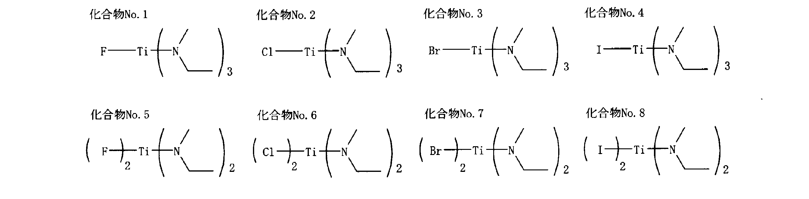
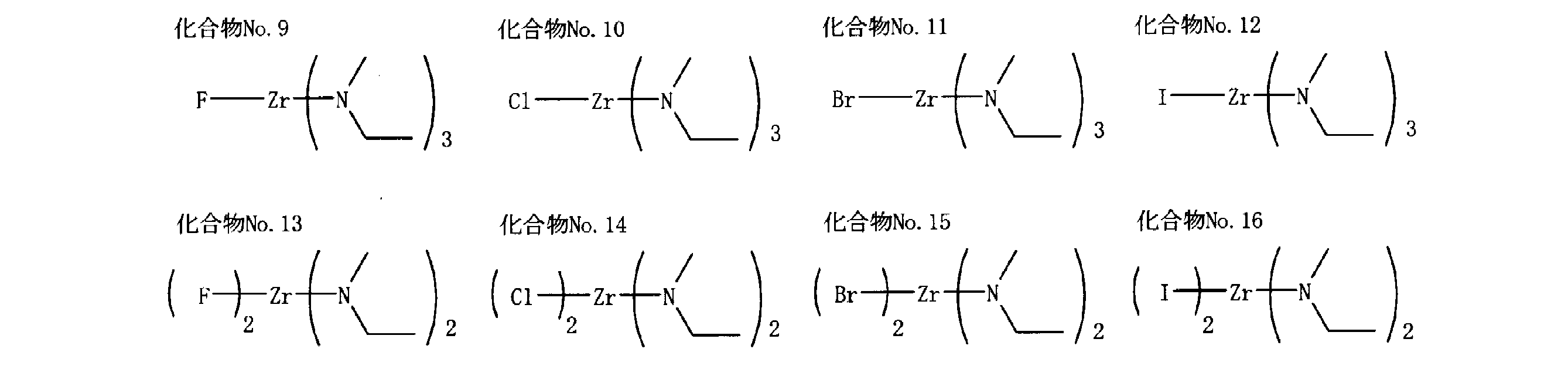
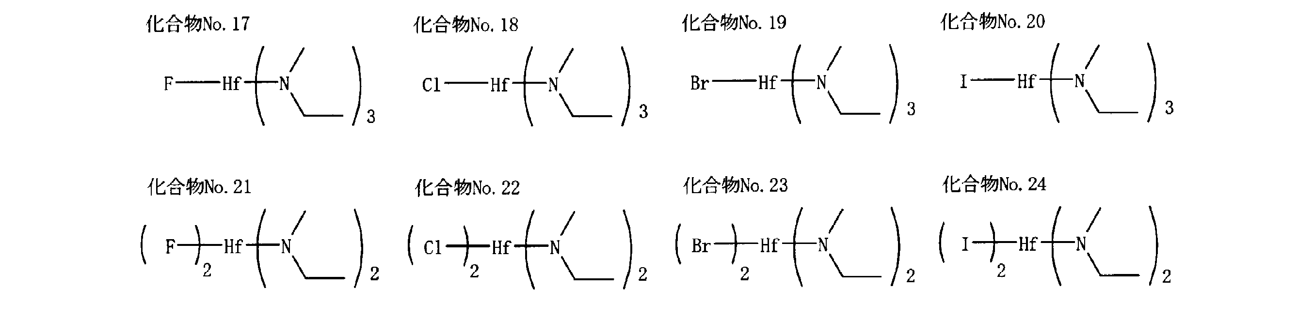
乾燥アルゴン雰囲気下で、反応フラスコに四塩化チタン(TiCl4)43.0g、脱水ヘキサン500mlを仕込み、-10℃まで冷却した。これにテトラキス(エチルメチルアミノ)チタン(Ti[N(CH3)(C2H5)]4)191gと脱水ヘキサン500mlの混合溶液を反応系が-5℃を越えないように滴下した。滴下終了後、室温で8時間攪拌した後、減圧下でヘキサンを留去した。残渣を減圧蒸留して、圧力100Pa、留出温度82℃のフラクションから目的物である化合物No.2を収率90%で得た。得られた化合物No.2の同定は、元素分析及び1H-NMRにより行った。それらの結果を以下に示す。
Ti;18.5質量%(理論値18.59質量%)
塩素;13.4質量%(理論値13.76質量%)
(2)1H-NMR(溶媒:重ベンゼン)(ケミカルシフト:多重度:H数比)
(3.096:s:3)(3.429:q:2)(1.003:t:3)
乾燥アルゴン雰囲気下で、反応フラスコに四塩化チタン(TiCl4)55.7g、脱水トルエン300mlを仕込み、-10℃まで冷却した。これにテトラキス(エチルメチルアミノ)チタン(Ti[N(CH3)(C2H5)]4)82.3gと脱水トルエン300mlの混合溶液を反応系が-5℃を越えないように滴下した。滴下終了後、室温で8時間攪拌した後、減圧下でトルエンを留去した。残渣を減圧蒸留して、圧力100Pa、留出温度85℃のフラクションから目的物である化合物No.6を収率90%で得た。得られた化合物No.6の同定は、元素分析及び1H-NMRにより行った。それらの結果を以下に示す。
Ti;20.3質量%(理論値20.38質量%)
塩素;30.1質量%(理論値30.17質量%)
(2)1H-NMR(溶媒:重ベンゼン)(ケミカルシフト:多重度:H数比)
(3.021:s:3)(3.470:q:2)(1.003:t:3)
上記の実施例1及び2で得た化合物No.2、6、表1、2に示す比較化合物について、20℃での状態(固体であれば融点:DTA測定による融点の吸熱開始温度)と熱分解性の評価を行った。これらの結果を表1又は表2に示す。熱分解性は、化合物をステンレス容器に密閉して、1時間加熱後の減圧下(10torr)でのTG-DTA測定の結果、0.5質量%を超える分解物が確認された場合の加熱温度である。加熱温度はTiCl4以外は80℃から10℃刻みで200℃までを選択し、TiCl4は、250℃~300℃を選択した。例えば、130℃、1時間加熱後の減圧下でのTG-DTA測定の結果、ほぼ全量が揮発しており、140℃、1時間過熱後の減圧下でのTG-DTA測定の結果、全量が揮発しないで、質量減少終了時に0.5質量%を超える残渣を生じた場合は、140℃とした。

適する。また、熱分解性は、TiCl4、Ti[N(CH3)(C2H5)]4よりも良好で
ある。このことは、より低温での薄膜製造を与えること、これをプレカーサとして得られる薄膜の膜質が良好であることを示唆するものである。特に、薄膜中の残留炭素による電気特性への影響が小さいので窒化チタンに代表されるLSIのゲート薄膜、バリア薄膜、電極膜の用途に好適であると考えられる。

上記実施例1で得た金属化合物No.2を化学気相成長用原料とし、図1に示す装置を用いて以下の条件のALD法により、シリコンウエハ上に窒化チタン薄膜を製造した。得られた薄膜について、蛍光X線による膜厚測定、薄膜組成の確認を行ったところ、膜厚は60nmであり、膜組成は窒化チタンであり、炭素含有量は1.3atom%であった。(条件)
反応温度(基板温度);300℃、反応性ガス;NH3
(工程)
下記(1)~(4)からなる一連の工程を1サイクルとして、300サイクル繰り返した。
(1)気化室温度:120℃、気化室圧力250Paの条件で気化させたCVD原料の蒸気を導入し、系圧 250Paで3秒間堆積させる。
(2)3秒間のアルゴンパージにより、未反応原料を除去する。
(3)反応性ガスを導入し、系圧力250Paで3秒間反応させる。
(4)2秒間のアルゴンパージにより、未反応原料を除去する。
Ti[N(CH3)(C2H5)]4を化学気相成長用原料とし、上記実施例2と同じ条件のALD法により、シリコンウエハ上に窒化チタン薄膜を製造した。得られた薄膜について、蛍光X線による膜厚測定、薄膜組成の確認を行ったところ、膜厚は50nmであり、膜組成は窒化チタンであり、炭素含有量は7.0atom%であった。
Claims (8)
- 下記一般式(1)で表される金属化合物。

- 上記一般式(1)において、Mがチタニウム原子である請求の範囲第1項に記載の金属化合物。
- 上記一般式(1)において、Xが塩素原子である請求の範囲第1又は2項に記載の金属化合物。
- 上記一般式(1)において、mが1である請求の範囲第1~3項の何れかに記載の金属化合物。
- 請求の範囲第1~4項の何れかに記載の金属化合物を含有してなる化学気相成長用原料。
- 基体上に窒化金属系薄膜を化学気相成長法により形成する原料である請求の範囲第5項に記載の化学気相成長用原料。
- 請求の範囲第5又は6項に記載の化学気相成長用原料を用いた化学気相成長法による金属含有薄膜の製造方法。
- 請求の範囲第6項に記載の化学気相成長用原料を用いた化学気相成長法による窒化金属系薄膜の製造方法。
Priority Applications (3)
| Application Number | Priority Date | Filing Date | Title |
|---|---|---|---|
| US12/740,188 US8357815B2 (en) | 2008-01-25 | 2008-10-22 | Metal compound, material for chemical vapor phase growth, and process for forming metal-containing thin film |
| CN2008801147932A CN101848917B (zh) | 2008-01-25 | 2008-10-22 | 金属化合物、含有其的化学气相沉积用原料以及含有金属的薄膜的制造方法 |
| EP08871220A EP2233491B1 (en) | 2008-01-25 | 2008-10-22 | Metal compound, chemical vapor deposition material containing the same, and method for producing metal-containing thin film |
Applications Claiming Priority (2)
| Application Number | Priority Date | Filing Date | Title |
|---|---|---|---|
| JP2008014791A JP5301169B2 (ja) | 2008-01-25 | 2008-01-25 | 金属化合物、これを含有してなる化学気相成長用原料及び金属含有薄膜の製造方法 |
| JP2008-014791 | 2008-01-25 |
Publications (1)
| Publication Number | Publication Date |
|---|---|
| WO2009093366A1 true WO2009093366A1 (ja) | 2009-07-30 |
Family
ID=40900882
Family Applications (1)
| Application Number | Title | Priority Date | Filing Date |
|---|---|---|---|
| PCT/JP2008/069121 Ceased WO2009093366A1 (ja) | 2008-01-25 | 2008-10-22 | 金属化合物、これを含有してなる化学気相成長用原料及び金属含有薄膜の製造方法 |
Country Status (7)
| Country | Link |
|---|---|
| US (1) | US8357815B2 (ja) |
| EP (1) | EP2233491B1 (ja) |
| JP (1) | JP5301169B2 (ja) |
| KR (1) | KR101569138B1 (ja) |
| CN (1) | CN101848917B (ja) |
| TW (1) | TWI419896B (ja) |
| WO (1) | WO2009093366A1 (ja) |
Families Citing this family (6)
| Publication number | Priority date | Publication date | Assignee | Title |
|---|---|---|---|---|
| US8440556B2 (en) * | 2010-12-22 | 2013-05-14 | Intel Corporation | Forming conformal metallic platinum zinc films for semiconductor devices |
| JP2012193445A (ja) * | 2011-02-28 | 2012-10-11 | Tokyo Electron Ltd | 窒化チタン膜の形成方法、窒化チタン膜の形成装置及びプログラム |
| EP2940025B1 (en) | 2012-12-25 | 2017-02-01 | Adeka Corporation | Aluminum compound, thin film-forming raw material, and method for producing thin film |
| KR102185249B1 (ko) * | 2014-01-20 | 2020-12-02 | 삼성디스플레이 주식회사 | 표시 장치 및 그 구동 방법 |
| KR102556277B1 (ko) * | 2018-04-23 | 2023-07-17 | 삼성디스플레이 주식회사 | 성막 장치 및 성막 방법 |
| US11286562B2 (en) * | 2018-06-08 | 2022-03-29 | Asm Ip Holding B.V. | Gas-phase chemical reactor and method of using same |
Citations (6)
| Publication number | Priority date | Publication date | Assignee | Title |
|---|---|---|---|---|
| JPH07201779A (ja) | 1993-12-28 | 1995-08-04 | Toshiba Corp | 電極配線およびその形成方法 |
| KR0156980B1 (ko) | 1995-06-23 | 1998-12-01 | 신현주 | 질화금속 박막증착용 화합물 및 그를 이용한 증착방법 |
| JP2000036473A (ja) | 1998-07-16 | 2000-02-02 | Nec Corp | 半導体装置の製造方法 |
| JP2003064475A (ja) | 2001-08-27 | 2003-03-05 | Asahi Denka Kogyo Kk | 化学気相成長用原料及びこれを用いた薄膜の製造方法 |
| JP2006045083A (ja) | 2004-08-02 | 2006-02-16 | Asahi Denka Kogyo Kk | 薄膜形成用原料、薄膜の製造方法及び金属化合物 |
| JP2006182709A (ja) | 2004-12-28 | 2006-07-13 | Adeka Corp | 薄膜形成用原料、薄膜の製造方法及び金属化合物 |
Family Cites Families (4)
| Publication number | Priority date | Publication date | Assignee | Title |
|---|---|---|---|---|
| US6831188B1 (en) * | 2002-07-31 | 2004-12-14 | Albemarle Corporation | Dihydrocarbylamino metal compounds |
| CN1898192A (zh) * | 2003-12-25 | 2007-01-17 | 株式会社艾迪科 | 金属化合物、薄膜形成用原料及薄膜的制造方法 |
| KR100581993B1 (ko) * | 2004-06-09 | 2006-05-22 | 삼성전자주식회사 | 원자층 증착법을 이용한 물질 형성방법 |
| US7250367B2 (en) * | 2004-09-01 | 2007-07-31 | Micron Technology, Inc. | Deposition methods using heteroleptic precursors |
-
2008
- 2008-01-25 JP JP2008014791A patent/JP5301169B2/ja active Active
- 2008-10-22 KR KR1020107009857A patent/KR101569138B1/ko active Active
- 2008-10-22 EP EP08871220A patent/EP2233491B1/en not_active Not-in-force
- 2008-10-22 US US12/740,188 patent/US8357815B2/en active Active
- 2008-10-22 WO PCT/JP2008/069121 patent/WO2009093366A1/ja not_active Ceased
- 2008-10-22 CN CN2008801147932A patent/CN101848917B/zh active Active
- 2008-10-30 TW TW097141862A patent/TWI419896B/zh active
Patent Citations (6)
| Publication number | Priority date | Publication date | Assignee | Title |
|---|---|---|---|---|
| JPH07201779A (ja) | 1993-12-28 | 1995-08-04 | Toshiba Corp | 電極配線およびその形成方法 |
| KR0156980B1 (ko) | 1995-06-23 | 1998-12-01 | 신현주 | 질화금속 박막증착용 화합물 및 그를 이용한 증착방법 |
| JP2000036473A (ja) | 1998-07-16 | 2000-02-02 | Nec Corp | 半導体装置の製造方法 |
| JP2003064475A (ja) | 2001-08-27 | 2003-03-05 | Asahi Denka Kogyo Kk | 化学気相成長用原料及びこれを用いた薄膜の製造方法 |
| JP2006045083A (ja) | 2004-08-02 | 2006-02-16 | Asahi Denka Kogyo Kk | 薄膜形成用原料、薄膜の製造方法及び金属化合物 |
| JP2006182709A (ja) | 2004-12-28 | 2006-07-13 | Adeka Corp | 薄膜形成用原料、薄膜の製造方法及び金属化合物 |
Non-Patent Citations (1)
| Title |
|---|
| See also references of EP2233491A4 * |
Also Published As
| Publication number | Publication date |
|---|---|
| US20100247765A1 (en) | 2010-09-30 |
| EP2233491A4 (en) | 2011-05-25 |
| CN101848917A (zh) | 2010-09-29 |
| KR20100106950A (ko) | 2010-10-04 |
| EP2233491B1 (en) | 2012-07-11 |
| TW200936601A (en) | 2009-09-01 |
| JP2009173587A (ja) | 2009-08-06 |
| JP5301169B2 (ja) | 2013-09-25 |
| KR101569138B1 (ko) | 2015-11-13 |
| CN101848917B (zh) | 2013-02-27 |
| US8357815B2 (en) | 2013-01-22 |
| TWI419896B (zh) | 2013-12-21 |
| EP2233491A1 (en) | 2010-09-29 |
Similar Documents
| Publication | Publication Date | Title |
|---|---|---|
| JP5528762B2 (ja) | Ald用原料及びこれを用いたケイ素含有薄膜形成方法 | |
| JP6735163B2 (ja) | バナジウム化合物、薄膜形成用原料及び薄膜の製造方法 | |
| US20200140463A1 (en) | Metal alkoxide compound, thin film forming raw material, and thin film production method | |
| JP4632765B2 (ja) | アルコキシド化合物、薄膜形成用原料及び薄膜の製造方法 | |
| JP5301169B2 (ja) | 金属化合物、これを含有してなる化学気相成長用原料及び金属含有薄膜の製造方法 | |
| KR102791292B1 (ko) | 원자층 퇴적법용 박막 형성 원료, 박막의 제조 방법 및 알콕시드 화합물 | |
| TWI879816B (zh) | 新穎錫化合物、含有該化合物的薄膜形成用原料、使用該薄膜形成用原料所形成的薄膜、將作為前驅物的該化合物使用於製造該薄膜的方法,及該薄膜的製造方法 | |
| EP3643700A1 (en) | Metal alkoxide compound, thin-film-forming raw material, and method for producing thin film | |
| WO2019039103A1 (ja) | タングステン化合物、薄膜形成用原料及び薄膜の製造方法 | |
| WO2020170853A1 (ja) | 原子層堆積法用窒化ガリウム含有薄膜形成用原料及び窒化ガリウム含有薄膜の製造方法 | |
| JP5912911B2 (ja) | アルミニウム化合物を用いたald法による薄膜の製造方法 | |
| JP2006182709A (ja) | 薄膜形成用原料、薄膜の製造方法及び金属化合物 | |
| KR20230037573A (ko) | 알콕시드 화합물, 박막 형성용 원료 및 박막의 제조 방법 | |
| KR20220161372A (ko) | 아연 화합물, 박막 형성용 원료, 박막 및 그 제조 방법 | |
| JP6116007B2 (ja) | 薄膜形成用原料及び薄膜の製造方法 | |
| JP2011106008A (ja) | 化学気相成長用原料及びルテニウム化合物 | |
| JP4781012B2 (ja) | アルコール化合物を配位子とした金属化合物及び薄膜形成用原料並びに薄膜の製造方法 | |
| JP4711733B2 (ja) | 酸化珪素系薄膜の製造方法 | |
| JP7573514B2 (ja) | 薄膜形成用原料、薄膜の製造方法及び新規なスカンジウム化合物 | |
| JP4745137B2 (ja) | 薄膜形成用原料、薄膜の製造方法及びハフニウム化合物 | |
| JP2006312600A (ja) | 金属化合物、薄膜形成用原料、薄膜の製造方法及び薄膜 | |
| WO2022196491A1 (ja) | スズ化合物、薄膜形成用原料、薄膜、薄膜の製造方法及びハロゲン化合物 | |
| WO2023276716A1 (ja) | 薄膜形成用原料、薄膜及び薄膜の製造方法 | |
| KR20230117368A (ko) | 인듐 화합물, 박막 형성용 원료, 박막 및 그 제조 방법 |
Legal Events
| Date | Code | Title | Description |
|---|---|---|---|
| WWE | Wipo information: entry into national phase |
Ref document number: 200880114793.2 Country of ref document: CN |
|
| 121 | Ep: the epo has been informed by wipo that ep was designated in this application |
Ref document number: 08871220 Country of ref document: EP Kind code of ref document: A1 |
|
| WWE | Wipo information: entry into national phase |
Ref document number: 12740188 Country of ref document: US |
|
| WWE | Wipo information: entry into national phase |
Ref document number: 2008871220 Country of ref document: EP |
|
| ENP | Entry into the national phase |
Ref document number: 20107009857 Country of ref document: KR Kind code of ref document: A |
|
| NENP | Non-entry into the national phase |
Ref country code: DE |