WO2009096259A1 - プラズマ処理方法及びプラズマ処理装置 - Google Patents
プラズマ処理方法及びプラズマ処理装置 Download PDFInfo
- Publication number
- WO2009096259A1 WO2009096259A1 PCT/JP2009/050703 JP2009050703W WO2009096259A1 WO 2009096259 A1 WO2009096259 A1 WO 2009096259A1 JP 2009050703 W JP2009050703 W JP 2009050703W WO 2009096259 A1 WO2009096259 A1 WO 2009096259A1
- Authority
- WO
- WIPO (PCT)
- Prior art keywords
- plasma processing
- processing method
- bias power
- amount
- substrate
- Prior art date
- Legal status (The legal status is an assumption and is not a legal conclusion. Google has not performed a legal analysis and makes no representation as to the accuracy of the status listed.)
- Ceased
Links
Images


Classifications
-
- C—CHEMISTRY; METALLURGY
- C23—COATING METALLIC MATERIAL; COATING MATERIAL WITH METALLIC MATERIAL; CHEMICAL SURFACE TREATMENT; DIFFUSION TREATMENT OF METALLIC MATERIAL; COATING BY VACUUM EVAPORATION, BY SPUTTERING, BY ION IMPLANTATION OR BY CHEMICAL VAPOUR DEPOSITION, IN GENERAL; INHIBITING CORROSION OF METALLIC MATERIAL OR INCRUSTATION IN GENERAL
- C23C—COATING METALLIC MATERIAL; COATING MATERIAL WITH METALLIC MATERIAL; SURFACE TREATMENT OF METALLIC MATERIAL BY DIFFUSION INTO THE SURFACE, BY CHEMICAL CONVERSION OR SUBSTITUTION; COATING BY VACUUM EVAPORATION, BY SPUTTERING, BY ION IMPLANTATION OR BY CHEMICAL VAPOUR DEPOSITION, IN GENERAL
- C23C16/00—Chemical coating by decomposition of gaseous compounds, without leaving reaction products of surface material in the coating, i.e. chemical vapour deposition [CVD] processes
- C23C16/22—Chemical coating by decomposition of gaseous compounds, without leaving reaction products of surface material in the coating, i.e. chemical vapour deposition [CVD] processes characterised by the deposition of inorganic material, other than metallic material
- C23C16/30—Deposition of compounds, mixtures or solid solutions, e.g. borides, carbides, nitrides
- C23C16/34—Nitrides
- C23C16/345—Silicon nitride
-
- C—CHEMISTRY; METALLURGY
- C23—COATING METALLIC MATERIAL; COATING MATERIAL WITH METALLIC MATERIAL; CHEMICAL SURFACE TREATMENT; DIFFUSION TREATMENT OF METALLIC MATERIAL; COATING BY VACUUM EVAPORATION, BY SPUTTERING, BY ION IMPLANTATION OR BY CHEMICAL VAPOUR DEPOSITION, IN GENERAL; INHIBITING CORROSION OF METALLIC MATERIAL OR INCRUSTATION IN GENERAL
- C23C—COATING METALLIC MATERIAL; COATING MATERIAL WITH METALLIC MATERIAL; SURFACE TREATMENT OF METALLIC MATERIAL BY DIFFUSION INTO THE SURFACE, BY CHEMICAL CONVERSION OR SUBSTITUTION; COATING BY VACUUM EVAPORATION, BY SPUTTERING, BY ION IMPLANTATION OR BY CHEMICAL VAPOUR DEPOSITION, IN GENERAL
- C23C16/00—Chemical coating by decomposition of gaseous compounds, without leaving reaction products of surface material in the coating, i.e. chemical vapour deposition [CVD] processes
- C23C16/44—Chemical coating by decomposition of gaseous compounds, without leaving reaction products of surface material in the coating, i.e. chemical vapour deposition [CVD] processes characterised by the method of coating
- C23C16/50—Chemical coating by decomposition of gaseous compounds, without leaving reaction products of surface material in the coating, i.e. chemical vapour deposition [CVD] processes characterised by the method of coating using electric discharges
- C23C16/505—Chemical coating by decomposition of gaseous compounds, without leaving reaction products of surface material in the coating, i.e. chemical vapour deposition [CVD] processes characterised by the method of coating using electric discharges using radio frequency discharges
-
- H—ELECTRICITY
- H01—ELECTRIC ELEMENTS
- H01J—ELECTRIC DISCHARGE TUBES OR DISCHARGE LAMPS
- H01J37/00—Discharge tubes with provision for introducing objects or material to be exposed to the discharge, e.g. for the purpose of examination or processing thereof
- H01J37/32—Gas-filled discharge tubes
- H01J37/32009—Arrangements for generation of plasma specially adapted for examination or treatment of objects, e.g. plasma sources
- H01J37/32082—Radio frequency generated discharge
- H01J37/321—Radio frequency generated discharge the radio frequency energy being inductively coupled to the plasma
-
- H—ELECTRICITY
- H01—ELECTRIC ELEMENTS
- H01J—ELECTRIC DISCHARGE TUBES OR DISCHARGE LAMPS
- H01J37/00—Discharge tubes with provision for introducing objects or material to be exposed to the discharge, e.g. for the purpose of examination or processing thereof
- H01J37/32—Gas-filled discharge tubes
- H01J37/32431—Constructional details of the reactor
- H01J37/32697—Electrostatic control
- H01J37/32706—Polarising the substrate
-
- H—ELECTRICITY
- H10—SEMICONDUCTOR DEVICES; ELECTRIC SOLID-STATE DEVICES NOT OTHERWISE PROVIDED FOR
- H10P—GENERIC PROCESSES OR APPARATUS FOR THE MANUFACTURE OR TREATMENT OF DEVICES COVERED BY CLASS H10
- H10P14/00—Formation of materials, e.g. in the shape of layers or pillars
- H10P14/60—Formation of materials, e.g. in the shape of layers or pillars of insulating materials
- H10P14/63—Formation of materials, e.g. in the shape of layers or pillars of insulating materials characterised by the formation processes
- H10P14/6326—Deposition processes
- H10P14/6328—Deposition from the gas or vapour phase
- H10P14/6334—Deposition from the gas or vapour phase using decomposition or reaction of gaseous or vapour phase compounds, i.e. chemical vapour deposition
- H10P14/6336—Deposition from the gas or vapour phase using decomposition or reaction of gaseous or vapour phase compounds, i.e. chemical vapour deposition in the presence of a plasma [PECVD]
-
- H—ELECTRICITY
- H10—SEMICONDUCTOR DEVICES; ELECTRIC SOLID-STATE DEVICES NOT OTHERWISE PROVIDED FOR
- H10P—GENERIC PROCESSES OR APPARATUS FOR THE MANUFACTURE OR TREATMENT OF DEVICES COVERED BY CLASS H10
- H10P14/00—Formation of materials, e.g. in the shape of layers or pillars
- H10P14/60—Formation of materials, e.g. in the shape of layers or pillars of insulating materials
- H10P14/69—Inorganic materials
- H10P14/694—Inorganic materials composed of nitrides
- H10P14/6943—Inorganic materials composed of nitrides containing silicon
- H10P14/69433—Inorganic materials composed of nitrides containing silicon the material being a silicon nitride not containing oxygen, e.g. SixNy or SixByNz
Definitions
- the present invention relates to a plasma processing method and a plasma processing apparatus.
- Non-Patent Document 1 Non-Patent Document 2 below.
- the present invention provides a plasma processing method and a plasma processing apparatus capable of suppressing an increase in compressive stress and a decrease in Si—H / N—H bond due to bias power application and enabling embedded deposition of a SiN film.
- the purpose is to provide.
- a plasma processing method for solving the above-described problem is a plasma processing using plasma of a source gas containing silicon and hydrogen and a gas containing nitrogen (for example, nitrogen gas, ammonia gas, etc.).
- a source gas containing silicon and hydrogen and a gas containing nitrogen for example, nitrogen gas, ammonia gas, etc.
- the amount of Si—H bonds in the silicon nitride film is increased by setting a bias power for making ions incident on the substrate to be equal to or higher than a threshold value. It is characterized by reducing the compressive stress of the film.
- a plasma processing method according to a second aspect of the present invention for solving the above problem is the plasma processing method according to the first aspect of the present invention, wherein the amount of Si—H bonds is reduced by reducing the RF power applied to generate plasma. To reduce the compressive stress.
- a plasma processing method according to a third aspect of the present invention for solving the above problem is the plasma processing method according to the first aspect of the present invention, wherein the amount of Si—H bonds is increased by increasing the pressure to reduce the compressive stress. It is characterized by that.
- a plasma processing method according to a fourth aspect of the present invention for solving the above problem is the plasma processing method according to the first aspect of the present invention, wherein the Si—H bond amount is increased by increasing the supply amount of a nitrogen-containing gas. And compressive stress is reduced.
- a plasma processing method for solving the above-described problems is the plasma processing method according to the first aspect of the present invention, wherein the amount of Si—H bonds is increased by reducing the plasma processing temperature to reduce the compressive stress. It is characterized by reducing.
- a plasma processing method according to a sixth invention for solving the above-mentioned problems is characterized in that, in the plasma processing method according to the first invention, the threshold is 1.2 kW in the case of a 200 mm wafer.
- a plasma processing apparatus for solving the above-described problem is Gas supply amount control means for controlling the gas supply amount of the source gas containing silicon and hydrogen and the gas containing nitrogen supplied to the inside of the vacuum vessel; Pressure control means for controlling the pressure inside the vacuum vessel; Plasma generating means for generating plasma by applying RF power to the source gas and the nitrogen gas inside the vacuum vessel; A substrate holding means for holding a substrate to be plasma processed inside the vacuum vessel; Temperature control means for controlling the temperature during plasma processing of the substrate; Bias power applying means for applying bias power to the substrate; And a parameter control unit that reduces the compressive stress by increasing the amount of Si—H bonds by setting the bias power for making ions incident on the substrate to be equal to or greater than a threshold value.
- Si in the silicon nitride film is obtained.
- reducing the compressive stress of the silicon nitride film by increasing the amount of —H bonds film peeling due to an increase in the compressive stress of the SiN film when bias power is applied can be suppressed. Can be formed.
- FIG. 10 is a graph showing the experimental results of an experiment for measuring the Si—H / N—H amount when the bias power is changed. It is the figure which showed the microscope picture of the SiN film
- FIG. 1 is a configuration diagram of a plasma processing apparatus according to an embodiment of the present invention.
- the plasma processing apparatus 1 includes a vacuum vessel 10 that can maintain a high degree of vacuum.
- the vacuum vessel 10 includes a cylindrical vessel 11 and a ceiling plate 12, and a ceiling plate 12 is attached to the upper portion of the cylindrical vessel 11 to form a space sealed from outside air.
- the vacuum vessel 13 is provided with a vacuum device 13 that evacuates the inside of the vacuum vessel 10.
- An RF antenna 15 for generating plasma 14 is installed on the top of the ceiling plate 12.
- An RF power source 17 that is a high frequency power source is connected to the RF antenna 15 via a matching unit 16. That is, the RF power supplied from the RF power source 17 is supplied to the plasma 14 by the RF antenna 15.
- a raw material gas supply pipe 18 that supplies a raw material gas, which is a raw material of a film to be formed, into the vacuum container 10 is installed on the upper side wall of the cylindrical container 11.
- the source gas supply pipe 18 is provided with a source gas supply amount control valve 18a for controlling the supply amount of the source gas.
- SiH 4 is supplied as the source gas.
- the upper portion of the side wall of the cylindrical container 11, N 2 gas supplied into the vacuum chamber 10 with N 2 gas supply pipe 19 is installed.
- the N 2 gas supply pipe 19 N 2 gas supply amount control valve 19a for controlling the supply amount of N 2 gas is provided.
- An Ar supply pipe 20 that supplies Ar gas into the vacuum container 10 is installed on the upper portion of the side wall of the cylindrical container 11.
- the Ar gas supply pipe 20 is provided with an Ar gas supply amount control valve 20a for controlling the supply amount of Ar gas.
- SiH 4 , N 2, and Ar plasma 14 is generated above the inside of the vacuum chamber 10.
- the substrate support 22 includes a substrate holder 23 that holds the substrate 21 and a support shaft 24 that supports the substrate holder 23.
- a heater 25 for heating is installed inside the substrate holder 23, and the temperature of the heater 25 is adjusted by a heater control device 26. Thereby, the temperature of the substrate 21 during the plasma processing can be controlled.
- a bias power source 29 is connected to the substrate holding unit 23 via a capacitor 27 and a matching unit 28 so that bias power can be applied to the substrate 21. Thereby, ions can be drawn into the surface of the substrate 21 from the plasma 14. Furthermore, an electrostatic power supply 30 is connected to the substrate holding part 23 so that the substrate 21 can be held by electrostatic force.
- the RF power supply 17 and the bias power supply 29 are not connected to the electrostatic power supply 30 and are connected to the substrate holding unit 22 via a low-pass filter 31 (LPF) so that the power does not enter.
- LPF low-pass filter
- the bias power of the bias power source 29, the RF power of the RF power source 17, the pressure of the vacuum device 13, the heater control device 26, the source gas supply valve 18a, the N 2 gas supply valve 19a, and the Ar gas supply valve 20a A parameter control device 32 capable of controlling the gas supply amount is installed. 1 is controlled from the parameter control device to the bias power source 29, the RF power source 17, the vacuum device 13, the heater control device 26, the source gas supply valve 18a, the N 2 gas supply valve 19a, and the Ar gas supply valve 20a. It means a signal line for transmitting a signal.
- the parameter control device 32 controls the bias power, RF power, pressure, film formation temperature, and gas supply amount based on the conditions described later, so A membrane is possible.
- the parameter control device 32 in this embodiment performs control so as to reduce the compressive stress by increasing the amount of Si—H bonds especially by setting the bias power for making ions incident on the substrate 21 to be equal to or higher than the threshold value. It will be described in detail below that the compressive stress can be reduced by increasing the amount of Si—H bonds by setting the bias power for making ions incident on the substrate 21 to be equal to or greater than the threshold value.
- the substrate 21 (see FIG. 1) to be deposited is a 200 mm diameter wafer.
- the RF power (13.56 MHz) is 2 kW
- the flow rates of SiH 4 , N 2, and Ar are 50 sccm
- the pressure is 25 mTorr
- the film formation temperature is 250 ° C.
- the SiN film is formed.
- the film thickness was set to 350 nm.
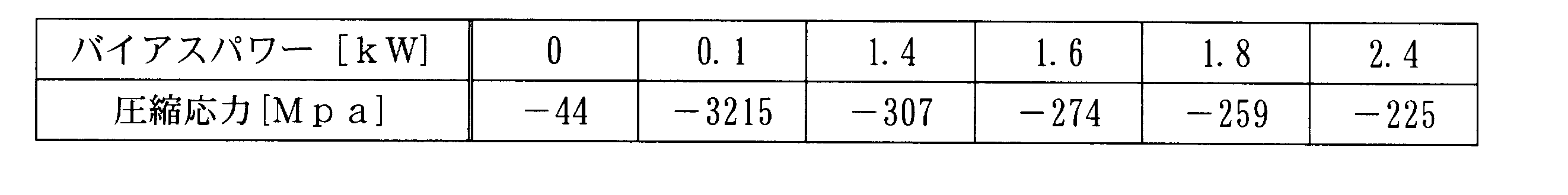
- Table 1 is a table showing experimental results of experiments for measuring the compressive stress of the SiN film when the bias power is changed.
- FIG. 2 is a graph showing the experimental results shown in Table 1.
- the compressive stress increases with the application of the bias power as before (0.1 kW is a maximum), but the compressive stress decreases as the bias power is further increased.
- the state of the SiN film was observed at each bias power, film peeling occurred at 1.6 kW or less, and no film peeling occurred at 1.8 kW or more. From this, it can be seen that in order to suppress the occurrence of film peeling, it is necessary to set the bias power to a certain threshold value or more. Therefore, in order to make the bias power equal to or higher than the threshold value, it is necessary to apply a bias power of 5.7 W / cm 2 or more per unit area (1.8 kW for a 200 mm wafer) to the substrate 21 (see FIG. 1).
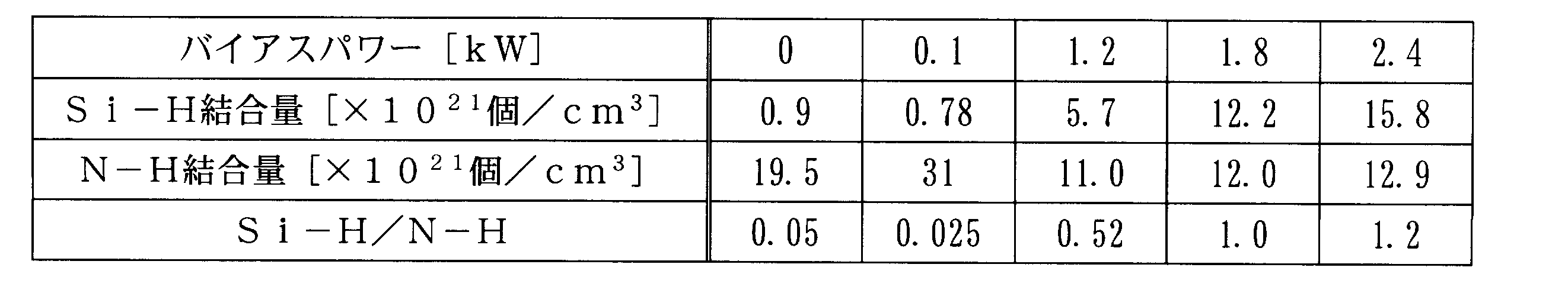
- Table 2 is a table showing experimental results of experiments for measuring the Si—H bond amount and N—H bond amount when the bias power is changed.
- FIG. 3 is a graph showing the measurement results of the Si—H / N—H amount when the bias power shown in Table 2 is changed.
- Si—H / N—H decreases as before until a bias power of 0.1 kW. However, when the bias power is further increased, the amount of Si—H coupling increases in proportion to the bias power. It can be seen that the amount of Si—H / N—H increases.
- FIG. 4 shows a micrograph of the SiN film formed with a bias power of 0.5 kW
- FIG. 5 shows a micrograph of the SiN film formed with a bias power of 1.6 kW
- FIG. 6 shows the bias. It is the figure which showed the microscope picture of the SiN film
- FIG. 4 when the bias power is 0.5 kW, it can be seen that film peeling occurs over the front surface of the substrate 21 (see FIG. 1). Note that the portion shown in the pattern in FIG. 4 is a portion where film peeling occurs. Further, as shown in FIG. 5, when the bias power is 1.6 kW, it can be seen that minute film peeling occurs. In addition, the part which is like the white dot enclosed by the broken line in FIG. 5 is a part in which film peeling has occurred.
- the compressive stress of the SiN film decreases and the Si—H / N—H amount increases when the bias power is set higher than the threshold value.
- the film density improvement and the compression stress increase due to the bias power (ion bombardment) up to the threshold value, and if the bias power is applied beyond that, the compressive stress is reduced due to the hydrogen drawing effect. That is, in the conventional technique, there was a problem of peeling of the film due to an increase in compressive stress even when trying to increase the bias power to form a SiN embedded film.
- the bias power is controlled to be higher than the threshold value, thereby attracting hydrogen. It has been found that the compressive stress is reduced due to the effect, thereby enabling embedded film formation.
- the substrate 21 (see FIG. 1) to be deposited is a 200 mm diameter wafer.
- the bias power (4 MHz) is 2.4 kW
- the RF power 13.56 MHz
- the flow rates of SiH 4 , N 2 and Ar are 50 sccm
- the pressure is 25 mTorr
- the film formation temperature was set at 250 ° C.
- Table 3 is a table showing experimental results of experiments for measuring compressive stress when the thickness of the SiN film to be formed is 350 nm and 10,000 nm.
- FIG. 7 is a graph showing the measurement results of the compressive stress when the thickness of the SiN film to be formed shown in Table 3 is changed between 350 nm and 10000 nm.
- the substrate 21 (see FIG. 1) to be deposited is a 200 mm diameter wafer.
- the process conditions for forming the SiN film are as follows: bias power (4 MHz) is 2.4 kW, RF power (13.56 MHz) is 2 kW, N 2 and Ar flow rates are 50 sccm, pressure is 25 mTorr, and film formation temperature is 250 ° C.
- the film thickness of the SiN film to be formed was set to 350 nm.
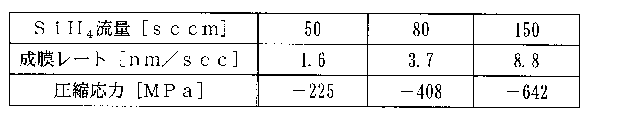
- Table 4 is a table showing experimental results of experiments for measuring the compressive stress of the SiN film when the deposition rate is changed.
- FIG. 8 is a graph showing the measurement result of the compressive stress of the SiN film when the film formation rate is changed as shown in Table 4.
- the substrate 21 (see FIG. 1) to be deposited is a 200 mm diameter wafer.
- the bias power (4 MHz) is 2.4 kW
- the RF power 13.56 MHz
- the flow rates of SiH 4 , N 2, and Ar are 50 sccm
- the pressure is 25 mTorr.
- the film thickness of the SiN film was set to 350 nm.
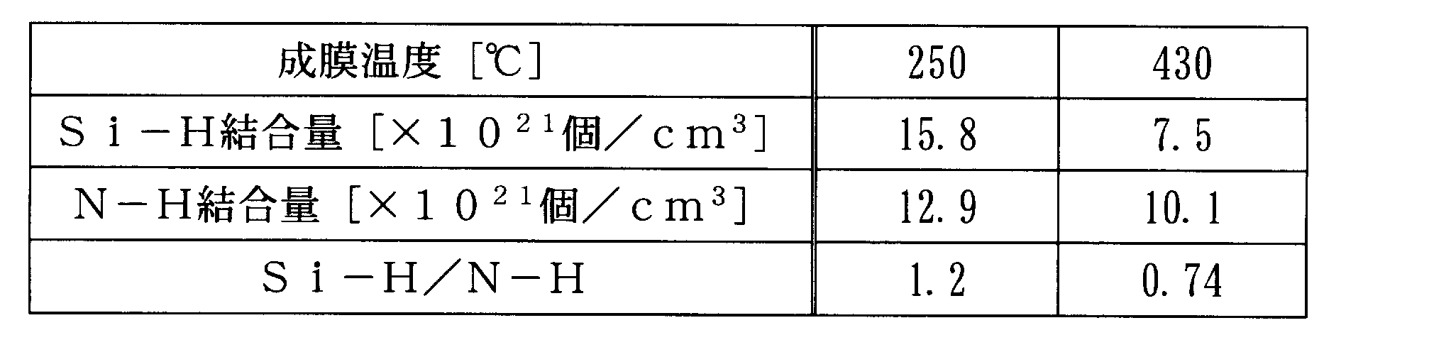
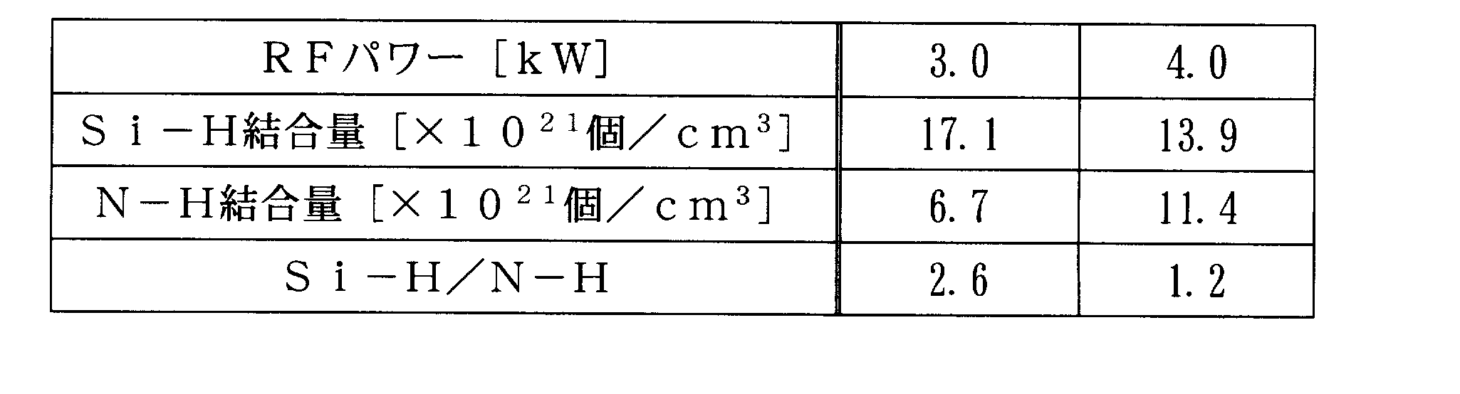
- Table 5 is a table showing experimental results of experiments for measuring the amount of Si—H bonds in the SiN film when the film forming temperature is changed.
- the Si—H bond amount increases as the film forming temperature decreases. For this reason, it can be seen that by controlling the film formation temperature, the amount of Si—H bonds can be controlled, so that the compressive stress of the SiN film can be controlled. That is, by lowering the film formation temperature, the amount of Si—H bonds can be increased, thereby reducing the compressive stress of SiN.
- the substrate 21 (see FIG. 1) to be deposited is a 200 mm diameter wafer.
- the bias power (4 MHz) is 2.4 kW
- the RF power 13.56 MHz
- the flow rate of Ar is 50 sccm
- the pressure is 25 mTorr
- the film formation temperature is 250 ° C.
- the film thickness of the SiN film was set to 350 nm.
- Table 6 is a table showing experimental results of an experiment for measuring the Si—H bond amount in the SiN film when the SiH 4 flow rate / N 2 flow rate is changed.
- the Si—H bond amount can be controlled by controlling the SiH 4 flow rate / N 2 flow rate, whereby the compressive stress of the SiN film can be controlled. That is, by increasing the SiH 4 flow rate / N 2 flow rate, the amount of Si—H bonds can be increased, thereby reducing the compressive stress of SiN.
- the substrate 21 (see FIG. 1) to be deposited is a 200 mm diameter wafer.
- the bias power (4 MHz) is 2.4 kW
- the flow rates of SiH 4 , N 2, and Ar are 50 sccm
- the pressure is 25 mTorr
- the film forming temperature is 250 ° C.
- the SiN film to be formed is formed.
- the film thickness was set to 350 nm.
- Table 7 is a table showing experimental results of experiments for measuring the amount of Si—H bonds in the SiN film when the RF power is changed.
- the Si—H bond amount increases as the RF power decreases. For this reason, it can be seen that the amount of Si—H bonds can be controlled by controlling the RF power, and thus the compressive stress of the SiN film can be controlled. That is, by reducing the RF power, the amount of Si—H bonds can be increased, thereby reducing the compressive stress of SiN.
- the substrate 21 (see FIG. 1) to be deposited is a 200 mm diameter wafer.
- the bias power (4 MHz) is 2.4 kW
- the RF power 13.56 MHz
- the flow rates of SiH 4 , N 2, and Ar are 50 sccm
- the film formation temperature is 250 ° C.
- the thickness of the SiN film to be formed was set to 350 nm.
- Table 8 is a table showing experimental results of experiments for measuring the amount of Si—H bonds in the SiN film when the pressure is changed.
- the Si—H bond amount increases as the pressure increases. For this reason, it can be seen that by controlling the pressure, the amount of Si—H bonds can be controlled, so that the compressive stress of the SiN film can be controlled. That is, by increasing the pressure, the amount of Si—H bonds can be increased, thereby reducing the compressive stress of SiN.
- the amount of Si—H groups (Si—H bond amount) in the SiN film and the compressive stress of the SiN film It was found that there is a negative correlation between the two.
- the amount of Si—H bonds in the SiN film is increased by controlling the bias power, RF power, pressure, film thickness, gas mixture ratio, and film formation temperature with the parameter control device 32 (see FIG. 1).
- the compressive stress of the SiN film it was possible to embed an SiN film by applying bias power.
- the parameter control device 32 has a process condition for forming the SiN film, the RF power (13.56 MHz) is 2 kW, the flow rates of SiH 4 , N 2, and Ar are 50 sccm, the pressure is 25 mTorr, and the film is formed.
- the bias power is set to 5.7 W / cm 2 per unit area on the substrate 21 (see FIG. 1) to be formed (for a 200 mm wafer).
- the bias power for example, application to an image sensor (CCD / CMOS) lens and waveguide by the high refractive index and high transmittance of the SiN film, and the barrier property of the SiN film.
- Application to the final protective film of the wiring In particular, by controlling the bias power, RF power, pressure, film thickness, gas mixture ratio, and film formation temperature, the amount of Si—H bonds in the film can be increased.
- Application to an image sensor known to reduce dark current by terminating is effective.
- the present invention can be used, for example, in a plasma processing method and a plasma processing apparatus that can embed a SiN film by applying bias power.
Landscapes
- Chemical & Material Sciences (AREA)
- Engineering & Computer Science (AREA)
- Physics & Mathematics (AREA)
- Plasma & Fusion (AREA)
- Metallurgy (AREA)
- Chemical Kinetics & Catalysis (AREA)
- Materials Engineering (AREA)
- Mechanical Engineering (AREA)
- General Chemical & Material Sciences (AREA)
- Organic Chemistry (AREA)
- Analytical Chemistry (AREA)
- Inorganic Chemistry (AREA)
- Formation Of Insulating Films (AREA)
- Chemical Vapour Deposition (AREA)
- Plasma Technology (AREA)
- Internal Circuitry In Semiconductor Integrated Circuit Devices (AREA)
Abstract
Description
真空容器の内部に供給するシリコン及び水素を含有する原料ガスと窒素を含有するガスのガス供給量を制御するガス供給量制御手段と、
前記真空容器の内部の圧力を制御する圧力制御手段と、
前記真空容器の内部の前記原料ガスと前記窒素ガスにRFパワーを印加してプラズマを発生させるプラズマ発生手段と、
前記真空容器の内部で、プラズマ処理対象となる基板を保持する基板保持手段と、
前記基板のプラズマ処理時の温度を制御する温度制御手段と、
前記基板にバイアスパワーを印加するバイアスパワー印加手段と、
前記基板にイオン入射させるバイアスパワーを閾値以上にすることでSi-H結合量を増加させて圧縮応力を低減させるパラメータ制御手段と
を備えた
ことを特徴とする。
図1は本発明の一実施形態に係るプラズマ処理装置の構成図である。図1に示すように、プラズマ処理装置1は、高い真空度を維持できる真空容器10を備えている。この真空容器10は、筒状容器11と天井板12からなり、筒状容器11の上部に天井板12を取り付けることで外気から密閉された空間を形成している。
第1の実験として、SiN膜成膜時において、バイアスパワーを変化させたときの、SiN膜の圧縮応力、Si-H結合量及びN-H結合量を測定する実験を行った。ここで、成膜処理対象の基板21(図1参照)は、200mm径のウェハとする。SiN膜成膜時のプロセス条件として、RFパワー(13.56MHz)は2kW、SiH4とN2とArの流量はそれぞれ50sccm、圧力は25mTorr、成膜温度は250℃、成膜するSiN膜の膜厚は350nmと設定した。


Claims (7)
- シリコン及び水素を含有する原料ガスと窒素を含有するガスとのプラズマにより、プラズマ処理対象の基板に対して窒化シリコン膜を成長させるプラズマ処理方法において、
前記基板にイオン入射させるバイアスパワーを閾値以上にすることでSi-H結合量を増加させて圧縮応力を低減させる
ことを特徴とするプラズマ処理方法。 - 請求項1に記載のプラズマ処理方法において、
プラズマを生成するために印加するRFパワーを減少させることでSi-H結合量を増加させて圧縮応力を低減させる
ことを特徴とするプラズマ処理方法。 - 請求項1に記載のプラズマ処理方法において、
圧力を高くすることでSi-H結合量を増加させて圧縮応力を低減させる
ことを特徴とするプラズマ処理方法。 - 請求項1に記載のプラズマ処理方法において、
前記原料ガスと窒素を含有するガスの供給量を増加させることでSi-H結合量を増加させて圧縮応力を低減させる
ことを特徴とするプラズマ処理方法。 - 請求項1に記載のプラズマ処理方法において、
プラズマ処理温度を低下させることでSi-H結合量を増加させて圧縮応力を低減させる
ことを特徴とするプラズマ処理方法。 - 請求項1に記載のプラズマ処理方法において、
前記閾値は、200mmウェハの場合1.2kWとする
ことを特徴とするプラズマ処理方法。 - 真空容器の内部に供給するシリコン及び水素を含有する原料ガスと窒素を含有するガスのガス供給量を制御するガス供給量制御手段と、
前記真空容器の内部の圧力を制御する圧力制御手段と、
前記真空容器の内部の前記原料ガスと前記窒素ガスにRFパワーを印加してプラズマを発生させるプラズマ発生手段と、
前記真空容器の内部で、プラズマ処理対象となる基板を保持する基板保持手段と、
前記基板のプラズマ処理時の温度を制御する温度制御手段と、
前記基板にバイアスパワーを印加するバイアスパワー印加手段と、
前記基板にイオン入射させるバイアスパワーを閾値以上にすることでSi-H結合量を増加させて圧縮応力を低減させるパラメータ制御手段と
を備えた
ことを特徴とするプラズマ処理装置。
Priority Applications (4)
| Application Number | Priority Date | Filing Date | Title |
|---|---|---|---|
| EP09705243.5A EP2242092A4 (en) | 2008-01-28 | 2009-01-20 | METHOD AND SYSTEM FOR PLASMA PROCESSING |
| KR1020107016842A KR101158377B1 (ko) | 2008-01-28 | 2009-01-20 | 플라즈마 처리 방법 및 플라즈마 처리 시스템 |
| US12/812,653 US20100310791A1 (en) | 2008-01-28 | 2009-01-20 | Plasma processing method and plasma processing system |
| US14/059,502 US20140057459A1 (en) | 2008-01-28 | 2013-10-22 | Plasma processing method and plasma processing system |
Applications Claiming Priority (2)
| Application Number | Priority Date | Filing Date | Title |
|---|---|---|---|
| JP2008-015894 | 2008-01-28 | ||
| JP2008015894A JP5297048B2 (ja) | 2008-01-28 | 2008-01-28 | プラズマ処理方法及びプラズマ処理装置 |
Related Child Applications (2)
| Application Number | Title | Priority Date | Filing Date |
|---|---|---|---|
| US12/812,653 A-371-Of-International US20100310791A1 (en) | 2008-01-28 | 2009-01-20 | Plasma processing method and plasma processing system |
| US14/059,502 Division US20140057459A1 (en) | 2008-01-28 | 2013-10-22 | Plasma processing method and plasma processing system |
Publications (1)
| Publication Number | Publication Date |
|---|---|
| WO2009096259A1 true WO2009096259A1 (ja) | 2009-08-06 |
Family
ID=40912612
Family Applications (1)
| Application Number | Title | Priority Date | Filing Date |
|---|---|---|---|
| PCT/JP2009/050703 Ceased WO2009096259A1 (ja) | 2008-01-28 | 2009-01-20 | プラズマ処理方法及びプラズマ処理装置 |
Country Status (6)
| Country | Link |
|---|---|
| US (2) | US20100310791A1 (ja) |
| EP (1) | EP2242092A4 (ja) |
| JP (1) | JP5297048B2 (ja) |
| KR (1) | KR101158377B1 (ja) |
| TW (1) | TW200947551A (ja) |
| WO (1) | WO2009096259A1 (ja) |
Cited By (3)
| Publication number | Priority date | Publication date | Assignee | Title |
|---|---|---|---|---|
| WO2011145489A1 (ja) * | 2010-05-21 | 2011-11-24 | 三菱重工業株式会社 | 半導体素子の窒化珪素膜、窒化珪素膜の製造方法及び装置 |
| EP2579301A4 (en) * | 2010-05-28 | 2013-12-18 | Mitsubishi Heavy Ind Ltd | METHOD AND DEVICE FOR PRODUCING A SILICON NITRIDE FILM |
| EP2579300A4 (en) * | 2010-05-28 | 2013-12-18 | Mitsubishi Heavy Ind Ltd | SILICON NITRIDE FILM FOR A SEMICONDUCTOR ELEMENT AND METHOD AND DEVICE FOR PRODUCING A SILICON NITRIDE FILM |
Families Citing this family (51)
| Publication number | Priority date | Publication date | Assignee | Title |
|---|---|---|---|---|
| JP5069597B2 (ja) * | 2008-03-27 | 2012-11-07 | 富士フイルム株式会社 | ガスバリアフィルムの製造方法 |
| US8728956B2 (en) | 2010-04-15 | 2014-05-20 | Novellus Systems, Inc. | Plasma activated conformal film deposition |
| US9076646B2 (en) | 2010-04-15 | 2015-07-07 | Lam Research Corporation | Plasma enhanced atomic layer deposition with pulsed plasma exposure |
| US9287113B2 (en) | 2012-11-08 | 2016-03-15 | Novellus Systems, Inc. | Methods for depositing films on sensitive substrates |
| US9390909B2 (en) | 2013-11-07 | 2016-07-12 | Novellus Systems, Inc. | Soft landing nanolaminates for advanced patterning |
| US9373500B2 (en) | 2014-02-21 | 2016-06-21 | Lam Research Corporation | Plasma assisted atomic layer deposition titanium oxide for conformal encapsulation and gapfill applications |
| US9257274B2 (en) | 2010-04-15 | 2016-02-09 | Lam Research Corporation | Gapfill of variable aspect ratio features with a composite PEALD and PECVD method |
| US9611544B2 (en) | 2010-04-15 | 2017-04-04 | Novellus Systems, Inc. | Plasma activated conformal dielectric film deposition |
| US9997357B2 (en) | 2010-04-15 | 2018-06-12 | Lam Research Corporation | Capped ALD films for doping fin-shaped channel regions of 3-D IC transistors |
| US8956983B2 (en) | 2010-04-15 | 2015-02-17 | Novellus Systems, Inc. | Conformal doping via plasma activated atomic layer deposition and conformal film deposition |
| US8637411B2 (en) | 2010-04-15 | 2014-01-28 | Novellus Systems, Inc. | Plasma activated conformal dielectric film deposition |
| US9892917B2 (en) | 2010-04-15 | 2018-02-13 | Lam Research Corporation | Plasma assisted atomic layer deposition of multi-layer films for patterning applications |
| US9685320B2 (en) | 2010-09-23 | 2017-06-20 | Lam Research Corporation | Methods for depositing silicon oxide |
| US8844793B2 (en) * | 2010-11-05 | 2014-09-30 | Raytheon Company | Reducing formation of oxide on solder |
| US8592328B2 (en) * | 2012-01-20 | 2013-11-26 | Novellus Systems, Inc. | Method for depositing a chlorine-free conformal sin film |
| US20140038421A1 (en) * | 2012-08-01 | 2014-02-06 | Taiwan Semiconductor Manufacturing Company, Ltd. | Deposition Chamber and Injector |
| JP2014060378A (ja) * | 2012-08-23 | 2014-04-03 | Tokyo Electron Ltd | シリコン窒化膜の成膜方法、有機電子デバイスの製造方法及びシリコン窒化膜の成膜装置 |
| TWI595112B (zh) | 2012-10-23 | 2017-08-11 | 蘭姆研究公司 | 次飽和之原子層沉積及保形膜沉積 |
| SG2013083241A (en) | 2012-11-08 | 2014-06-27 | Novellus Systems Inc | Conformal film deposition for gapfill |
| US9214334B2 (en) | 2014-02-18 | 2015-12-15 | Lam Research Corporation | High growth rate process for conformal aluminum nitride |
| US9478438B2 (en) | 2014-08-20 | 2016-10-25 | Lam Research Corporation | Method and apparatus to deposit pure titanium thin film at low temperature using titanium tetraiodide precursor |
| US9478411B2 (en) | 2014-08-20 | 2016-10-25 | Lam Research Corporation | Method to tune TiOx stoichiometry using atomic layer deposited Ti film to minimize contact resistance for TiOx/Ti based MIS contact scheme for CMOS |
| US9214333B1 (en) | 2014-09-24 | 2015-12-15 | Lam Research Corporation | Methods and apparatuses for uniform reduction of the in-feature wet etch rate of a silicon nitride film formed by ALD |
| US9589790B2 (en) | 2014-11-24 | 2017-03-07 | Lam Research Corporation | Method of depositing ammonia free and chlorine free conformal silicon nitride film |
| US9564312B2 (en) | 2014-11-24 | 2017-02-07 | Lam Research Corporation | Selective inhibition in atomic layer deposition of silicon-containing films |
| US10566187B2 (en) | 2015-03-20 | 2020-02-18 | Lam Research Corporation | Ultrathin atomic layer deposition film accuracy thickness control |
| US9502238B2 (en) | 2015-04-03 | 2016-11-22 | Lam Research Corporation | Deposition of conformal films by atomic layer deposition and atomic layer etch |
| US10526701B2 (en) | 2015-07-09 | 2020-01-07 | Lam Research Corporation | Multi-cycle ALD process for film uniformity and thickness profile modulation |
| US9601693B1 (en) | 2015-09-24 | 2017-03-21 | Lam Research Corporation | Method for encapsulating a chalcogenide material |
| US9773643B1 (en) | 2016-06-30 | 2017-09-26 | Lam Research Corporation | Apparatus and method for deposition and etch in gap fill |
| US10062563B2 (en) | 2016-07-01 | 2018-08-28 | Lam Research Corporation | Selective atomic layer deposition with post-dose treatment |
| CN107665800B (zh) * | 2016-07-28 | 2019-06-07 | 中微半导体设备(上海)股份有限公司 | 一种用于等离子处理器的射频电源控制装置及其控制方法 |
| US10629435B2 (en) | 2016-07-29 | 2020-04-21 | Lam Research Corporation | Doped ALD films for semiconductor patterning applications |
| US10037884B2 (en) | 2016-08-31 | 2018-07-31 | Lam Research Corporation | Selective atomic layer deposition for gapfill using sacrificial underlayer |
| US10074543B2 (en) | 2016-08-31 | 2018-09-11 | Lam Research Corporation | High dry etch rate materials for semiconductor patterning applications |
| US9865455B1 (en) | 2016-09-07 | 2018-01-09 | Lam Research Corporation | Nitride film formed by plasma-enhanced and thermal atomic layer deposition process |
| US10454029B2 (en) | 2016-11-11 | 2019-10-22 | Lam Research Corporation | Method for reducing the wet etch rate of a sin film without damaging the underlying substrate |
| US10832908B2 (en) | 2016-11-11 | 2020-11-10 | Lam Research Corporation | Self-aligned multi-patterning process flow with ALD gapfill spacer mask |
| US10134579B2 (en) | 2016-11-14 | 2018-11-20 | Lam Research Corporation | Method for high modulus ALD SiO2 spacer |
| US10269559B2 (en) | 2017-09-13 | 2019-04-23 | Lam Research Corporation | Dielectric gapfill of high aspect ratio features utilizing a sacrificial etch cap layer |
| US11404275B2 (en) | 2018-03-02 | 2022-08-02 | Lam Research Corporation | Selective deposition using hydrolysis |
| KR20240160679A (ko) | 2019-05-01 | 2024-11-11 | 램 리써치 코포레이션 | 변조된 원자 층 증착 |
| WO2020247977A1 (en) | 2019-06-04 | 2020-12-10 | Lam Research Corporation | Polymerization protective liner for reactive ion etch in patterning |
| US12431349B2 (en) | 2019-06-07 | 2025-09-30 | Lam Research Corporation | In-situ control of film properties during atomic layer deposition |
| WO2021025874A1 (en) | 2019-08-06 | 2021-02-11 | Lam Research Corporation | Thermal atomic layer deposition of silicon-containing films |
| WO2021053987A1 (ja) * | 2019-09-20 | 2021-03-25 | 株式会社Kokusai Electric | 半導体装置の製造方法、基板処理装置、およびプログラム |
| CN115803474A (zh) | 2020-07-23 | 2023-03-14 | 朗姆研究公司 | 具有受控膜性质和高沉积速率的保形热cvd |
| KR20230043795A (ko) | 2020-07-28 | 2023-03-31 | 램 리써치 코포레이션 | 실리콘-함유 막들의 불순물 감소 |
| JP2022080674A (ja) * | 2020-11-18 | 2022-05-30 | 東京エレクトロン株式会社 | プラズマ処理装置 |
| WO2023283144A1 (en) | 2021-07-09 | 2023-01-12 | Lam Research Corporation | Plasma enhanced atomic layer deposition of silicon-containing films |
| US20240110284A1 (en) * | 2022-09-30 | 2024-04-04 | Applied Materials, Inc. | Selective Deposition of Thin Films with Improved Stability |
Citations (5)
| Publication number | Priority date | Publication date | Assignee | Title |
|---|---|---|---|---|
| JPH04297033A (ja) * | 1990-05-28 | 1992-10-21 | Fuji Electric Co Ltd | 窒化シリコン膜の形成方法 |
| JPH08115912A (ja) * | 1994-10-14 | 1996-05-07 | Nippon Telegr & Teleph Corp <Ntt> | 窒化ケイ素薄膜の作製方法 |
| JPH10209151A (ja) * | 1997-01-20 | 1998-08-07 | Nec Corp | 半導体装置の製造方法 |
| JP2003297830A (ja) * | 2002-04-03 | 2003-10-17 | Hitachi Kokusai Electric Inc | 半導体装置の製造方法 |
| JP2005079254A (ja) * | 2003-08-29 | 2005-03-24 | Mitsubishi Heavy Ind Ltd | 窒化シリコン膜の成膜方法 |
Family Cites Families (45)
| Publication number | Priority date | Publication date | Assignee | Title |
|---|---|---|---|---|
| US6068784A (en) * | 1989-10-03 | 2000-05-30 | Applied Materials, Inc. | Process used in an RF coupled plasma reactor |
| US6090303A (en) * | 1991-06-27 | 2000-07-18 | Applied Materials, Inc. | Process for etching oxides in an electromagnetically coupled planar plasma apparatus |
| US6024826A (en) * | 1996-05-13 | 2000-02-15 | Applied Materials, Inc. | Plasma reactor with heated source of a polymer-hardening precursor material |
| KR100281345B1 (ko) * | 1992-12-01 | 2001-03-02 | 조셉 제이. 스위니 | 전자기 결합성 플래너 플라즈마 장치에서의 산화물 에칭 공정 |
| US5571366A (en) * | 1993-10-20 | 1996-11-05 | Tokyo Electron Limited | Plasma processing apparatus |
| US5777289A (en) * | 1995-02-15 | 1998-07-07 | Applied Materials, Inc. | RF plasma reactor with hybrid conductor and multi-radius dome ceiling |
| US6270617B1 (en) * | 1995-02-15 | 2001-08-07 | Applied Materials, Inc. | RF plasma reactor with hybrid conductor and multi-radius dome ceiling |
| JPH0982495A (ja) * | 1995-09-18 | 1997-03-28 | Toshiba Corp | プラズマ生成装置およびプラズマ生成方法 |
| JPH09106899A (ja) * | 1995-10-11 | 1997-04-22 | Anelva Corp | プラズマcvd装置及び方法並びにドライエッチング装置及び方法 |
| EP0777258A3 (en) * | 1995-11-29 | 1997-09-17 | Applied Materials Inc | Self-cleaning plasma processing reactor |
| US5965034A (en) * | 1995-12-04 | 1999-10-12 | Mc Electronics Co., Ltd. | High frequency plasma process wherein the plasma is executed by an inductive structure in which the phase and anti-phase portion of the capacitive currents between the inductive structure and the plasma are balanced |
| US6902683B1 (en) * | 1996-03-01 | 2005-06-07 | Hitachi, Ltd. | Plasma processing apparatus and plasma processing method |
| US5683548A (en) * | 1996-02-22 | 1997-11-04 | Motorola, Inc. | Inductively coupled plasma reactor and process |
| TW335517B (en) * | 1996-03-01 | 1998-07-01 | Hitachi Ltd | Apparatus and method for processing plasma |
| US6009830A (en) * | 1997-11-21 | 2000-01-04 | Applied Materials Inc. | Independent gas feeds in a plasma reactor |
| US6136165A (en) * | 1997-11-26 | 2000-10-24 | Cvc Products, Inc. | Apparatus for inductively-coupled-plasma-enhanced ionized physical-vapor deposition |
| CN1161820C (zh) * | 1998-07-31 | 2004-08-11 | 佳能株式会社 | 半导体层制造方法和制造设备、光生伏打电池的制造方法 |
| TW465017B (en) * | 1999-04-13 | 2001-11-21 | Applied Materials Inc | A corrosion-resistant protective coating for an apparatus and method for processing a substrate |
| US6318384B1 (en) * | 1999-09-24 | 2001-11-20 | Applied Materials, Inc. | Self cleaning method of forming deep trenches in silicon substrates |
| US7141757B2 (en) * | 2000-03-17 | 2006-11-28 | Applied Materials, Inc. | Plasma reactor with overhead RF source power electrode having a resonance that is virtually pressure independent |
| US7220937B2 (en) * | 2000-03-17 | 2007-05-22 | Applied Materials, Inc. | Plasma reactor with overhead RF source power electrode with low loss, low arcing tendency and low contamination |
| US7223676B2 (en) * | 2002-06-05 | 2007-05-29 | Applied Materials, Inc. | Very low temperature CVD process with independently variable conformality, stress and composition of the CVD layer |
| US7294563B2 (en) * | 2000-08-10 | 2007-11-13 | Applied Materials, Inc. | Semiconductor on insulator vertical transistor fabrication and doping process |
| US6939434B2 (en) * | 2000-08-11 | 2005-09-06 | Applied Materials, Inc. | Externally excited torroidal plasma source with magnetic control of ion distribution |
| US7320734B2 (en) * | 2000-08-11 | 2008-01-22 | Applied Materials, Inc. | Plasma immersion ion implantation system including a plasma source having low dissociation and low minimum plasma voltage |
| US7137354B2 (en) * | 2000-08-11 | 2006-11-21 | Applied Materials, Inc. | Plasma immersion ion implantation apparatus including a plasma source having low dissociation and low minimum plasma voltage |
| US7037813B2 (en) * | 2000-08-11 | 2006-05-02 | Applied Materials, Inc. | Plasma immersion ion implantation process using a capacitively coupled plasma source having low dissociation and low minimum plasma voltage |
| US20020197402A1 (en) * | 2000-12-06 | 2002-12-26 | Chiang Tony P. | System for depositing a film by modulated ion-induced atomic layer deposition (MII-ALD) |
| US7871676B2 (en) * | 2000-12-06 | 2011-01-18 | Novellus Systems, Inc. | System for depositing a film by modulated ion-induced atomic layer deposition (MII-ALD) |
| US6667248B2 (en) * | 2001-09-05 | 2003-12-23 | Applied Materials Inc. | Low-bias-deposited high-density-plasma chemical-vapor-deposition silicate glass layers |
| US6926926B2 (en) * | 2001-09-10 | 2005-08-09 | Applied Materials, Inc. | Silicon carbide deposited by high density plasma chemical-vapor deposition with bias |
| US20030091739A1 (en) * | 2001-11-14 | 2003-05-15 | Hitoshi Sakamoto | Barrier metal film production apparatus, barrier metal film production method, metal film production method, and metal film production apparatus |
| US7169255B2 (en) * | 2002-02-15 | 2007-01-30 | Hitachi High-Technologies Corporation | Plasma processing apparatus |
| US6962644B2 (en) * | 2002-03-18 | 2005-11-08 | Applied Materials, Inc. | Tandem etch chamber plasma processing system |
| JP3840147B2 (ja) * | 2002-06-21 | 2006-11-01 | キヤノン株式会社 | 成膜装置、成膜方法およびそれを用いた電子放出素子、電子源、画像形成装置の製造方法 |
| US20040188240A1 (en) * | 2003-03-28 | 2004-09-30 | Taiwan Semiconductor Manufacturing Co., Ltd. | Process for in-situ nitridation of salicides |
| EP1793418B1 (en) * | 2004-07-02 | 2013-06-12 | Ulvac, Inc. | Etching method and system |
| US7399943B2 (en) * | 2004-10-05 | 2008-07-15 | Applied Materials, Inc. | Apparatus for metal plasma vapor deposition and re-sputter with source and bias power frequencies applied through the workpiece |
| US7271110B2 (en) * | 2005-01-05 | 2007-09-18 | Chartered Semiconductor Manufacturing, Ltd. | High density plasma and bias RF power process to make stable FSG with less free F and SiN with less H to enhance the FSG/SiN integration reliability |
| US20060162661A1 (en) * | 2005-01-22 | 2006-07-27 | Applied Materials, Inc. | Mixing energized and non-energized gases for silicon nitride deposition |
| US7820020B2 (en) * | 2005-02-03 | 2010-10-26 | Applied Materials, Inc. | Apparatus for plasma-enhanced physical vapor deposition of copper with RF source power applied through the workpiece with a lighter-than-copper carrier gas |
| US20070091540A1 (en) * | 2005-10-20 | 2007-04-26 | Applied Materials, Inc. | Method of processing a workpiece in a plasma reactor using multiple zone feed forward thermal control |
| US7473623B2 (en) * | 2006-06-30 | 2009-01-06 | Advanced Micro Devices, Inc. | Providing stress uniformity in a semiconductor device |
| JP2008047620A (ja) * | 2006-08-11 | 2008-02-28 | Mitsubishi Heavy Ind Ltd | プラズマ処理方法、及び、プラズマ処理装置 |
| US7871828B2 (en) * | 2007-02-06 | 2011-01-18 | Applied Materials, Inc. | In-situ dose monitoring using optical emission spectroscopy |
-
2008
- 2008-01-28 JP JP2008015894A patent/JP5297048B2/ja not_active Expired - Fee Related
-
2009
- 2009-01-20 EP EP09705243.5A patent/EP2242092A4/en not_active Withdrawn
- 2009-01-20 WO PCT/JP2009/050703 patent/WO2009096259A1/ja not_active Ceased
- 2009-01-20 US US12/812,653 patent/US20100310791A1/en not_active Abandoned
- 2009-01-20 KR KR1020107016842A patent/KR101158377B1/ko not_active Expired - Fee Related
- 2009-01-22 TW TW098102593A patent/TW200947551A/zh not_active IP Right Cessation
-
2013
- 2013-10-22 US US14/059,502 patent/US20140057459A1/en not_active Abandoned
Patent Citations (5)
| Publication number | Priority date | Publication date | Assignee | Title |
|---|---|---|---|---|
| JPH04297033A (ja) * | 1990-05-28 | 1992-10-21 | Fuji Electric Co Ltd | 窒化シリコン膜の形成方法 |
| JPH08115912A (ja) * | 1994-10-14 | 1996-05-07 | Nippon Telegr & Teleph Corp <Ntt> | 窒化ケイ素薄膜の作製方法 |
| JPH10209151A (ja) * | 1997-01-20 | 1998-08-07 | Nec Corp | 半導体装置の製造方法 |
| JP2003297830A (ja) * | 2002-04-03 | 2003-10-17 | Hitachi Kokusai Electric Inc | 半導体装置の製造方法 |
| JP2005079254A (ja) * | 2003-08-29 | 2005-03-24 | Mitsubishi Heavy Ind Ltd | 窒化シリコン膜の成膜方法 |
Non-Patent Citations (3)
| Title |
|---|
| C. W. PEARCE; R. F. FETCHO; M. D. GROSS; R. F. KOEFER; R. A. PUDLINER: "Characteristics of silicon nitride deposited by plasma-enhanced chemical vapor deposition using a dual frequency radio-frequency source", J. APPL. PHYS., vol. 71, no. 4, 15 February 1992 (1992-02-15), pages 1838 - 1841 |
| See also references of EP2242092A4 |
| TATSURU SHIRAFUJI, GAS PHASE/SURFACE REACTIONS OF PLASMA-ENHANCED CVD, 16 January 2008 (2008-01-16), Retrieved from the Internet <URL:http://shira.iic.kyoto-u.ac.jp/2006-09-02-PECVD-Lecture.pdf> |
Cited By (7)
| Publication number | Priority date | Publication date | Assignee | Title |
|---|---|---|---|---|
| WO2011145489A1 (ja) * | 2010-05-21 | 2011-11-24 | 三菱重工業株式会社 | 半導体素子の窒化珪素膜、窒化珪素膜の製造方法及び装置 |
| JP2011243889A (ja) * | 2010-05-21 | 2011-12-01 | Mitsubishi Heavy Ind Ltd | 半導体素子の窒化珪素膜、窒化珪素膜の製造方法及び装置 |
| EP2573803A4 (en) * | 2010-05-21 | 2013-12-18 | Mitsubishi Heavy Ind Ltd | SILICON NITRIDE FILM FOR A SEMICONDUCTOR COMPONENT AND METHOD AND DEVICE FOR PRODUCING THE SILICON NITRIDE FILM |
| KR101346863B1 (ko) | 2010-05-21 | 2014-01-02 | 미츠비시 쥬고교 가부시키가이샤 | 반도체 소자의 질화규소막, 질화규소막의 제조 방법 및 장치 |
| EP2579301A4 (en) * | 2010-05-28 | 2013-12-18 | Mitsubishi Heavy Ind Ltd | METHOD AND DEVICE FOR PRODUCING A SILICON NITRIDE FILM |
| EP2579300A4 (en) * | 2010-05-28 | 2013-12-18 | Mitsubishi Heavy Ind Ltd | SILICON NITRIDE FILM FOR A SEMICONDUCTOR ELEMENT AND METHOD AND DEVICE FOR PRODUCING A SILICON NITRIDE FILM |
| US8889568B2 (en) | 2010-05-28 | 2014-11-18 | Mitsubishi Heavy Industries, Ltd. | Method and apparatus for producing silicon nitride film |
Also Published As
| Publication number | Publication date |
|---|---|
| JP2009177046A (ja) | 2009-08-06 |
| JP5297048B2 (ja) | 2013-09-25 |
| US20140057459A1 (en) | 2014-02-27 |
| TWI373807B (ja) | 2012-10-01 |
| EP2242092A4 (en) | 2014-02-05 |
| US20100310791A1 (en) | 2010-12-09 |
| EP2242092A1 (en) | 2010-10-20 |
| KR20100098575A (ko) | 2010-09-07 |
| KR101158377B1 (ko) | 2012-06-25 |
| TW200947551A (en) | 2009-11-16 |
Similar Documents
| Publication | Publication Date | Title |
|---|---|---|
| JP5297048B2 (ja) | プラズマ処理方法及びプラズマ処理装置 | |
| JP5269093B2 (ja) | 低ウェットエッチング速度の窒化シリコン膜 | |
| TWI804693B (zh) | 用於隔離結構的伸縮襯裡層 | |
| KR102084296B1 (ko) | 성막 방법, 붕소 막 및 성막 장치 | |
| US20090242511A1 (en) | Seasoning method for film-forming apparatus | |
| CN107104036A (zh) | 用于在沟槽侧壁或平整表面上选择性形成氮化硅膜的方法 | |
| JP2005079254A (ja) | 窒化シリコン膜の成膜方法 | |
| CN103540908A (zh) | 沉积二氧化硅薄膜的方法 | |
| KR102007019B1 (ko) | 플라즈마 처리에 의한 불화 알루미늄 경감 | |
| US20180148833A1 (en) | Methods for depositing flowable silicon containing films using hot wire chemical vapor deposition | |
| KR101422981B1 (ko) | 질화 규소막의 제조 방법 및 장치 | |
| JP6220409B2 (ja) | プラズマエッチング方法 | |
| CN110835748B (zh) | 沉积氮化硅的方法和设备 | |
| Kim et al. | Effect of seasoning-layer stress on fluorine diffusion | |
| CN110318034A (zh) | 硼系膜的成膜方法和成膜装置 | |
| JP5495940B2 (ja) | 半導体素子の窒化珪素膜、窒化珪素膜の製造方法及び装置 | |
| US9637819B2 (en) | Methods for preferential growth of cobalt within substrate features | |
| WO2011148830A1 (ja) | 半導体素子の窒化珪素膜、窒化珪素膜の製造方法及び装置 | |
| TW201831723A (zh) | 成膜方法、硼膜、及成膜裝置 | |
| TW202434758A (zh) | 保形及選擇性的氮化矽沉積 | |
| TW202528579A (zh) | 使用用於間隙填充的羥基化進行接縫效能改善 |
Legal Events
| Date | Code | Title | Description |
|---|---|---|---|
| 121 | Ep: the epo has been informed by wipo that ep was designated in this application |
Ref document number: 09705243 Country of ref document: EP Kind code of ref document: A1 |
|
| WWE | Wipo information: entry into national phase |
Ref document number: 2009705243 Country of ref document: EP |
|
| ENP | Entry into the national phase |
Ref document number: 20107016842 Country of ref document: KR Kind code of ref document: A |
|
| NENP | Non-entry into the national phase |
Ref country code: DE |
|
| WWE | Wipo information: entry into national phase |
Ref document number: 12812653 Country of ref document: US |