WO2009096476A1 - 切削工具 - Google Patents
切削工具 Download PDFInfo
- Publication number
- WO2009096476A1 WO2009096476A1 PCT/JP2009/051483 JP2009051483W WO2009096476A1 WO 2009096476 A1 WO2009096476 A1 WO 2009096476A1 JP 2009051483 W JP2009051483 W JP 2009051483W WO 2009096476 A1 WO2009096476 A1 WO 2009096476A1
- Authority
- WO
- WIPO (PCT)
- Prior art keywords
- coating layer
- ratio
- cutting
- layer
- thickness
- Prior art date
- Legal status (The legal status is an assumption and is not a legal conclusion. Google has not performed a legal analysis and makes no representation as to the accuracy of the status listed.)
- Ceased
Links
Images


Classifications
-
- B—PERFORMING OPERATIONS; TRANSPORTING
- B23—MACHINE TOOLS; METAL-WORKING NOT OTHERWISE PROVIDED FOR
- B23C—MILLING
- B23C5/00—Milling-cutters
- B23C5/16—Milling-cutters characterised by physical features other than shape
- B23C5/20—Milling-cutters characterised by physical features other than shape with removable cutter bits or teeth or cutting inserts
- B23C5/202—Plate-like cutting inserts with special form
-
- B—PERFORMING OPERATIONS; TRANSPORTING
- B23—MACHINE TOOLS; METAL-WORKING NOT OTHERWISE PROVIDED FOR
- B23B—TURNING; BORING
- B23B51/00—Tools for drilling machines
-
- C—CHEMISTRY; METALLURGY
- C23—COATING METALLIC MATERIAL; COATING MATERIAL WITH METALLIC MATERIAL; CHEMICAL SURFACE TREATMENT; DIFFUSION TREATMENT OF METALLIC MATERIAL; COATING BY VACUUM EVAPORATION, BY SPUTTERING, BY ION IMPLANTATION OR BY CHEMICAL VAPOUR DEPOSITION, IN GENERAL; INHIBITING CORROSION OF METALLIC MATERIAL OR INCRUSTATION IN GENERAL
- C23C—COATING METALLIC MATERIAL; COATING MATERIAL WITH METALLIC MATERIAL; SURFACE TREATMENT OF METALLIC MATERIAL BY DIFFUSION INTO THE SURFACE, BY CHEMICAL CONVERSION OR SUBSTITUTION; COATING BY VACUUM EVAPORATION, BY SPUTTERING, BY ION IMPLANTATION OR BY CHEMICAL VAPOUR DEPOSITION, IN GENERAL
- C23C14/00—Coating by vacuum evaporation, by sputtering or by ion implantation of the coating forming material
- C23C14/06—Coating by vacuum evaporation, by sputtering or by ion implantation of the coating forming material characterised by the coating material
- C23C14/0641—Nitrides
-
- C—CHEMISTRY; METALLURGY
- C23—COATING METALLIC MATERIAL; COATING MATERIAL WITH METALLIC MATERIAL; CHEMICAL SURFACE TREATMENT; DIFFUSION TREATMENT OF METALLIC MATERIAL; COATING BY VACUUM EVAPORATION, BY SPUTTERING, BY ION IMPLANTATION OR BY CHEMICAL VAPOUR DEPOSITION, IN GENERAL; INHIBITING CORROSION OF METALLIC MATERIAL OR INCRUSTATION IN GENERAL
- C23C—COATING METALLIC MATERIAL; COATING MATERIAL WITH METALLIC MATERIAL; SURFACE TREATMENT OF METALLIC MATERIAL BY DIFFUSION INTO THE SURFACE, BY CHEMICAL CONVERSION OR SUBSTITUTION; COATING BY VACUUM EVAPORATION, BY SPUTTERING, BY ION IMPLANTATION OR BY CHEMICAL VAPOUR DEPOSITION, IN GENERAL
- C23C14/00—Coating by vacuum evaporation, by sputtering or by ion implantation of the coating forming material
- C23C14/06—Coating by vacuum evaporation, by sputtering or by ion implantation of the coating forming material characterised by the coating material
- C23C14/0664—Carbonitrides
-
- C—CHEMISTRY; METALLURGY
- C23—COATING METALLIC MATERIAL; COATING MATERIAL WITH METALLIC MATERIAL; CHEMICAL SURFACE TREATMENT; DIFFUSION TREATMENT OF METALLIC MATERIAL; COATING BY VACUUM EVAPORATION, BY SPUTTERING, BY ION IMPLANTATION OR BY CHEMICAL VAPOUR DEPOSITION, IN GENERAL; INHIBITING CORROSION OF METALLIC MATERIAL OR INCRUSTATION IN GENERAL
- C23C—COATING METALLIC MATERIAL; COATING MATERIAL WITH METALLIC MATERIAL; SURFACE TREATMENT OF METALLIC MATERIAL BY DIFFUSION INTO THE SURFACE, BY CHEMICAL CONVERSION OR SUBSTITUTION; COATING BY VACUUM EVAPORATION, BY SPUTTERING, BY ION IMPLANTATION OR BY CHEMICAL VAPOUR DEPOSITION, IN GENERAL
- C23C30/00—Coating with metallic material characterised only by the composition of the metallic material, i.e. not characterised by the coating process
- C23C30/005—Coating with metallic material characterised only by the composition of the metallic material, i.e. not characterised by the coating process on hard metal substrates
-
- B—PERFORMING OPERATIONS; TRANSPORTING
- B23—MACHINE TOOLS; METAL-WORKING NOT OTHERWISE PROVIDED FOR
- B23B—TURNING; BORING
- B23B2200/00—Details of cutting inserts
- B23B2200/08—Rake or top surfaces
- B23B2200/082—Rake or top surfaces with elevated clamping surface
-
- B—PERFORMING OPERATIONS; TRANSPORTING
- B23—MACHINE TOOLS; METAL-WORKING NOT OTHERWISE PROVIDED FOR
- B23B—TURNING; BORING
- B23B2251/00—Details of tools for drilling machines
- B23B2251/50—Drilling tools comprising cutting inserts
-
- B—PERFORMING OPERATIONS; TRANSPORTING
- B23—MACHINE TOOLS; METAL-WORKING NOT OTHERWISE PROVIDED FOR
- B23C—MILLING
- B23C2200/00—Details of milling cutting inserts
- B23C2200/08—Rake or top surfaces
- B23C2200/085—Rake or top surfaces discontinuous
-
- B—PERFORMING OPERATIONS; TRANSPORTING
- B23—MACHINE TOOLS; METAL-WORKING NOT OTHERWISE PROVIDED FOR
- B23C—MILLING
- B23C2224/00—Materials of tools or workpieces composed of a compound including a metal
- B23C2224/22—Titanium aluminium carbide nitride (TiAlCN)
-
- B—PERFORMING OPERATIONS; TRANSPORTING
- B23—MACHINE TOOLS; METAL-WORKING NOT OTHERWISE PROVIDED FOR
- B23C—MILLING
- B23C2224/00—Materials of tools or workpieces composed of a compound including a metal
- B23C2224/32—Titanium carbide nitride (TiCN)
-
- B—PERFORMING OPERATIONS; TRANSPORTING
- B23—MACHINE TOOLS; METAL-WORKING NOT OTHERWISE PROVIDED FOR
- B23C—MILLING
- B23C2228/00—Properties of materials of tools or workpieces, materials of tools or workpieces applied in a specific manner
- B23C2228/10—Coating
-
- Y—GENERAL TAGGING OF NEW TECHNOLOGICAL DEVELOPMENTS; GENERAL TAGGING OF CROSS-SECTIONAL TECHNOLOGIES SPANNING OVER SEVERAL SECTIONS OF THE IPC; TECHNICAL SUBJECTS COVERED BY FORMER USPC CROSS-REFERENCE ART COLLECTIONS [XRACs] AND DIGESTS
- Y10—TECHNICAL SUBJECTS COVERED BY FORMER USPC
- Y10T—TECHNICAL SUBJECTS COVERED BY FORMER US CLASSIFICATION
- Y10T407/00—Cutters, for shaping
- Y10T407/27—Cutters, for shaping comprising tool of specific chemical composition
-
- Y—GENERAL TAGGING OF NEW TECHNOLOGICAL DEVELOPMENTS; GENERAL TAGGING OF CROSS-SECTIONAL TECHNOLOGIES SPANNING OVER SEVERAL SECTIONS OF THE IPC; TECHNICAL SUBJECTS COVERED BY FORMER USPC CROSS-REFERENCE ART COLLECTIONS [XRACs] AND DIGESTS
- Y10—TECHNICAL SUBJECTS COVERED BY FORMER USPC
- Y10T—TECHNICAL SUBJECTS COVERED BY FORMER US CLASSIFICATION
- Y10T428/00—Stock material or miscellaneous articles
- Y10T428/24—Structurally defined web or sheet [e.g., overall dimension, etc.]
- Y10T428/24942—Structurally defined web or sheet [e.g., overall dimension, etc.] including components having same physical characteristic in differing degree
- Y10T428/2495—Thickness [relative or absolute]
- Y10T428/24967—Absolute thicknesses specified
- Y10T428/24975—No layer or component greater than 5 mils thick
-
- Y—GENERAL TAGGING OF NEW TECHNOLOGICAL DEVELOPMENTS; GENERAL TAGGING OF CROSS-SECTIONAL TECHNOLOGIES SPANNING OVER SEVERAL SECTIONS OF THE IPC; TECHNICAL SUBJECTS COVERED BY FORMER USPC CROSS-REFERENCE ART COLLECTIONS [XRACs] AND DIGESTS
- Y10—TECHNICAL SUBJECTS COVERED BY FORMER USPC
- Y10T—TECHNICAL SUBJECTS COVERED BY FORMER US CLASSIFICATION
- Y10T428/00—Stock material or miscellaneous articles
- Y10T428/25—Web or sheet containing structurally defined element or component and including a second component containing structurally defined particles
- Y10T428/252—Glass or ceramic [i.e., fired or glazed clay, cement, etc.] [porcelain, quartz, etc.]
Definitions
- the present invention relates to a cutting tool in which a coating layer is formed on the surface of a substrate.
- cutting tools require wear resistance, slidability, and fracture resistance. Therefore, various coating layers are formed on the surface of a hard substrate such as a WC-based cemented carbide or TiCN-based cermet, and the cutting tool is formed. A technique for improving the wear resistance and fracture resistance of steel is used.
- TiCN layers and TiAlN layers are generally widely used, but various coating layers are being developed for the purpose of improving higher wear resistance and fracture resistance.
- Patent Document 1 regarding the X-ray diffraction of the TiAl composite compound layer covering the surface of the substrate, the ratio I between the diffraction intensity I (111) of the (111) plane and the diffraction intensity I (200) of the (200) plane A throwaway insert in which the value of (200) / I (111) is controlled to 1 or more is disclosed. Further, in Patent Document 2, in order to improve the oxidation resistance and peel resistance of the coating layer, the diffraction intensity in the X-ray diffraction of the TiAl composite compound layer is set to a value of Ib (220) / Ia (111) of 1.0 ⁇ A throwaway insert having a range of Ib / Ia ⁇ 5.0 is disclosed.
- Patent Document 3 in the TiAlCr composite nitride or carbonitride coating layer, the peak intensity ratio of (111), (200), (220) crystal planes measured by X-ray diffraction can be controlled. Are listed. In the X-ray diffraction chart described in FIG. 6 in this document, there is almost no diffraction peak on the (400) plane. Patent Document 4 describes that a TiAl nitride layer has a stacked structure of a first layer having a maximum (200) crystal plane and a second layer having a maximum height (111) crystal plane. ing.
- the characteristics of the coating layer are controlled by controlling the diffraction intensity in the X-ray diffraction in the TiAl composite nitride layer, in particular, (111), (200) and ( 220) It is known that controlling the diffraction intensity of the crystal plane increases the hardness and oxidation resistance of the coating layer and also improves the adhesion to the substrate.
- the wear resistance does not improve even if the hardness and oxidation of the coating layer are simply increased.
- the coating layer is partially peeled, resulting in a problem that the life of the cutting tool cannot be extended.
- An object of the present invention is to provide a cutting tool having a long tool life even under cutting conditions requiring wear resistance and peeling resistance such as wet cutting.
- the cutting tool of the present invention is a coating layer made of a base and a nitride or carbonitride containing Ti and Al covering the surface of the base, the layer thickness at the flank being 3 to 9 ⁇ m, and
- the ratio I (400) / I (311) of the diffraction intensity I (400) of the (400) plane and the diffraction intensity I (311) of the (311) plane for the thin film X-ray diffraction peak of Cu—K ⁇ ray is p.
- the coating layer is composed of a lower layer and an upper layer, and an X of the Cu—K ⁇ line of the coating layer on the polished surface obtained by polishing the coating layer obliquely with respect to the thickness direction.
- P 1 measured on the polished surface is 0.1 to 0.5
- P 3 measured on the polished surface where the interface between the lower layer and the upper layer is exposed is P measured on the polished surface of the upper layer. It may be smaller than 2 and P 2 may be smaller than P 1 .
- the total thickness T e of the cutting edge of the coating layer becomes 3 ⁇ 15 [mu] m
- the ratio to the thickness T f of the coating layer at the center position of the flank is 1 .2 to 3.8 is desirable.
- the ratio of the lower layer of a thickness t e of total thickness T e of the coating layer in the cutting edge of the (t e / T e) and A is 0.2-0.6
- the ratio of the ratio A to the ratio a (A / A) is preferably 0.4 to 0.9.
- the layer thickness of the coating layer at the cutting edge is 3 to 10 ⁇ m, and (111), (X) about the micro X-ray diffraction peak of Cu—K ⁇ ray of the coating layer. 200), (220), (222), and (400) planes, the ratio I (220) / with respect to the diffraction intensities I (111), I (200), I (220), I (222), and I (400), respectively.
- the ratio I (400) / (I (111) + I (200) + I (220) + I (222) + I (400)) relating to I (400) is Q
- the Q value at the rake face is Q r
- the clearance When the Q value on the surface is Q f and the Q value on the cutting edge is Q e , it is desirable that Q r > Q e > Q f .
- a coating layer made of a nitride or carbonitride containing Ti and Al is coated on the surface of the substrate with a layer thickness of 3 to 9 ⁇ m on the flank surface, and Cu—K ⁇ rays in the coating layer are formed.
- the ratio I (400) / I (311) between the diffraction intensity I (400) of the (400) plane and the diffraction intensity I (311) of the (311) plane with respect to the thin film X-ray diffraction peak is p
- a major feature is that p in the layer is larger on the outer surface side than on the substrate side.
- p b By being 0.1 to 0.5, the adhesion can be enhanced.
- the coating layer is composed of a multilayer structure of the lower layer and the upper layer, and may be configured to control the alignment direction (P 1, P 2, P 3).
- the coating layer is composed of a multilayer structure of the lower layer and the upper layer, and may be configured to control the alignment direction (P 1, P 2, P 3).
- the total thickness T e of the cutting edge of the coating layer becomes 3 ⁇ 15 [mu] m, the ratio to the thickness T f of the coating layer at the center position of the flank (T e / T f) is 1.2-3
- the wear resistance can be enhanced without impairing the fracture resistance of the cutting edge.
- the ratio of the lower layer of a thickness t e of total thickness T e of the coating layer in the cutting edge of the (t e / T e) when the A, together with the ratio A is 0.2-0.6
- the ratio of the ratio A to the ratio a (A / a) Is preferably from 0.4 to 0.9 in terms of further suppressing the peeling of the coating layer on the cutting edge.
- the layer thickness of the coating layer at the cutting edge is 3 to 10 ⁇ m, and (111), (X) about the micro X-ray diffraction peak of the Cu—K ⁇ ray of the coating layer. 200), (220), (222), and (400) planes, the ratio I (220) / with respect to the diffraction intensities I (111), I (200), I (220), I (222), and I (400), respectively.
- High wear resistance is required for both the rake face and flank face, but since it is an impact load at the start of cutting and during interrupted machining, it is desirable that chipping resistance and fracture resistance are not lost especially on the rake face. .
- q e > q r > q f is desirable for improving the welding resistance at the time of cutting.
- the ratio I (400) / (I (111) + I (200) + I (220) + I (222) + I (400)) for I (400) is Q
- the Q value on the rake face is Qr
- the Q value on the flank face is When Qf is Qe at the cutting edge, Qr> Qe> Qf enables thickening without causing chipping or peeling due to impact at the time of cutting, and exhibits excellent wear resistance. Desirable for.
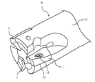
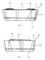
- FIG. 1 is a perspective view
- FIG. 2A is a schematic perspective view of a chip 1 to be mounted
- FIG. 2B is a plan view
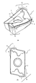
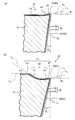
- FIG. 2 is a cross-sectional view of the chip 1 taken along the line aa in FIG. 3 and FIG.
- FIG. 3 are X-ray diffraction when thin film X-ray diffraction measurement is performed in a state where (s) the outer surface and (b) a layer thickness region within 1.5 ⁇ m are exposed from the substrate.
- FIG. 4 is an example of the pattern.
- the tip 1 has a main surface that forms the rake face 3 and a side face that forms the flank 4 of the substrate 2 whose main surface has a substantially flat plate shape.
- a cutting edge 8 having a cutting edge 6 and a sub-cutting edge 7 is formed, and the surface of the substrate 2 is covered with a coating layer 9.
- the chip 1 is mounted in the chip pocket 12 of the holder 11. And the chip
- a coating layer 9 made of a nitride or carbonitride containing Ti and Al and having a layer thickness of 3 to 9 ⁇ m on the flank face is coated.
- p in the coating layer 9 is larger on the outer surface side than on the substrate 2 side. This makes it possible to provide a cutting tool having high tool life and high wear resistance and excellent chipping resistance without peeling off the coating layer even in wet cutting. In particular, it is possible to greatly suppress the progress of boundary damage that is likely to occur during milling.
- the layer thickness on the flank face of the coating layer 9 is less than 3 ⁇ m, the wear resistance is drastically lowered, and wear progresses due to boundary damage and the tool life is reached.
- the layer thickness on the flank of the coating layer 9 exceeds 10 ⁇ m, the coating layer 9 is likely to be partially peeled off, and wear may progress from the peeling to reach the tool life early.
- a desirable range of the layer thickness of the coating layer 9 is 5 to 8 ⁇ m.
- the wear resistance of the chip 1 is lowered, and boundary damage particularly occurs in cutting processing such as milling wet cutting. Easy tool life.
- p b By being 0.1 to 0.5, the adhesion of the coating layer 9 to the substrate 2 is improved.
- r 1.5 ⁇ 7 is desirable. That is, when r is within this range, the progress of wear of the coating layer 9 is slow, and the occurrence of minute peeling or the like of the coating layer 9 can be suppressed.
- the honing 10 can be provided on the corner cutting edge 5.
- the shape of the honing 10 is desirably R honing in order to suppress peeling of the coating layer 9, but may be C honing (Chanhwa honing).
- honing amount, it ratio R r / R f of the rake face 3 side R r and the flank 4 side R f is 1 to 1.5 in view of the sharpness and chipping resistance in cutting edge 5 desirable.
- the fact that the main cutting edge 6 side as the bottom edge is large and the secondary cutting edge 7 side as the outer edge is small realizes a configuration suitable for the cutting environment at each position of the cutting edge 8 and exhibits optimum cutting performance. Desirable because it can.
- the coating layer 9 is formed by the sputtering method has a smooth surface and high resistance to welding, and self-destructs even when the internal stress in the coating layer 9 is small and the layer thickness is increased. This is desirable in that the chipping and peeling of the coating layer 9 are less likely to occur.
- the covering layer 9 may be composed of simple Ti 1-a Al a N, for example, Ti 1-ab Al a M b (C x N 1-x ) (where M Is one or more selected from Group 4, 5, 6 elements of the periodic table excluding Ti, rare earth elements, and Si, and 0 ⁇ a ⁇ 1, 0 ⁇ b ⁇ 1, and 0 ⁇ x ⁇ 1. It may be configured.
- the composition of the coating layer 9 can be measured by energy dispersive X-ray spectroscopy (EDS) analysis or X-ray photoelectron spectroscopy (XPS).
- tungsten carbide, a cemented carbide or cermet composed of a hard phase mainly composed of titanium carbonitride and a binder phase mainly composed of an iron group metal such as cobalt and nickel, silicon nitride, ,
- Hard materials such as ceramics mainly composed of aluminum oxide, hard phases made of polycrystalline diamond or cubic boron nitride, and bonded phases such as ceramics and iron group metals under super high pressure, etc. are preferably used.
- the cutting tool of the present invention can be used as a cutting tool under various cutting conditions.
- it is a wet cutting condition in which cutting is performed while using a cutting oil, and in particular, milling including end milling and drilling. Show excellent wear resistance and fracture resistance.
- a tool-shaped substrate is produced using a conventionally known method.
- a coating layer is formed on the surface of the substrate.
- PVD physical vapor deposition
- a physical vapor deposition (PVD) method such as an ion plating method or a sputtering method can be suitably applied as the coating layer forming method.
- metal titanium Ti
- metal aluminum Al
- metal M where M is a periodic table excluding Ti.
- One or more selected from Group 4, 5, 6 elements, rare earth elements and Si are used independently for metal targets or composite alloy targets.
- the metal source is evaporated and ionized by arc discharge or glow discharge, and at the same time, nitrogen (N 2 ) gas as a nitrogen source or methane (CH 4 ) / acetylene (C) as a carbon source.
- nitrogen (N 2 ) gas as a nitrogen source or methane (CH 4 ) / acetylene (C) as a carbon source.
- Conditions for reacting with 2 H 2 ) gas can be suitably employed.
- the deposition temperature is increased by an ion plating method or a sputtering method using a mixed gas of nitrogen (N 2 ) gas and argon (Ar) gas at an argon gas flow rate of 1: 9 to 4: 6.
- the coating layer is formed at 450 to 550 ° C., sputtering power of 6 kW to 9 kW, or bias voltage of 30 to 200 V. According to the present invention, it is possible to form a uniform structure without the occurrence of abnormal parts such as droplets generated when the film is formed by the arc ion plating method to be coated by the sputtering method. Is desirable. In addition, since the internal stress is low, even if the layer thickness is increased, the chipping resistance tends not to decrease due to the accumulation of internal stress. Therefore, a thicker film can be formed, brittle peeling during processing is suppressed, and the effect of improving wear resistance by surface coating can be exhibited.
- the above-described configuration of the coating layer can be achieved by controlling the rotation speed of the sample so as to be higher in the later stage of film formation than in the earlier stage of film formation.
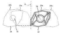
- FIG. 6 is a schematic side view showing the drill according to the present embodiment.
- FIG. 7 is a schematic front view of the drill of FIG. 6 as viewed from the tip.
- FIG. 8 is a schematic diagram for explaining the arrangement of the outer blades and the inner blades when cutting using the drill of FIG. 6.
- the insert shown with a broken line has shown the position when the insert shown with a continuous line rotates 180 degree
- the drill 21 has two throwaway inserts (hereinafter simply referred to as inserts) 23 to be described later at the tip of the tool body 22 whose center is the rotation axis O. Each one is attached.
- One insert 23 a is attached by a screw 24 so that the inner blade 25 protrudes from the tip of the tool body 22, and the other insert 23 b is radially outside the insert 23 a at the tip of the tool body 22 and is the tool body 22.
- the outer blade 26 is mounted by a screw 24 so as to protrude from the outer peripheral direction of the tool body 22 to the tip of the tool body 22. That is, the insert 23 a from which the inner blade 25 projects from the tool body 22 is provided on the radially inner side of the insert 23 b from which the outer blade 26 projects from the tool body 22.
- the tool main body 22 has a substantially cylindrical shape, has a rotating shaft of the drill 21 (line O in FIGS. 6 to 8), and has a shank portion 28 for fixing itself to the machine tool on the rear end side.
- a chip discharge groove 29 for discharging chips from the front end to the rear end of the tool body 22 is formed in a spiral shape on the front end side of the shank portion 28.
- insert pockets 30 (30a, 30b) for attaching the insert 23 are provided at two positions at the distal end portion of the tool body 22, and the inner insert pocket 30a is opened to the distal end side in the axial direction of the tool body 22.
- the insert 23a is mounted, and the outer insert pocket 30b is opened from the tip end side in the axial direction of the tool body 22 to the outer blade, and the insert 23b is mounted.
- the inner blade 25 cuts the inner peripheral side of the hole bottom surface of the work material (not shown), and the outer blade 26 cuts the hole bottom outer side and outer peripheral surface of the work material (not shown). 7 and 8, as shown in FIGS. 7 and 8, the rotation trajectories of the inner blade 25 and the outer blade 26 cross each other so that both cutting blades cover the tip to the outer periphery of the drill 21. Yes.
- FIG. 9 is a plan view showing the insert of this embodiment.
- FIG. 10 is the side view which looked at the insert of FIG. 9 from the (a) arrow A side, and (b) is the side view seen from the arrow B side.
- FIG. 11 is an enlarged view showing a cross section taken along line II of the insert shown in FIG. 9 and an enlarged view showing a cross section taken along line II-II of FIG.
- the insert 23 according to the embodiment shown in FIGS. 9 to 11 has a substantially polygonal plate shape when viewed from above, and a through hole 34 is formed at the center of the upper surface 31. As shown in FIG. 11, the insert 23 has a coating layer 36 formed on the surface of the base 35, and the inner ridge line portion 41 between the upper surface 31 and the side surface 32 of the insert 23 is adjacent to each other. A blade 25 and an outer blade 26 are formed.
- the covering layer 36 made of a nitride or carbonitride containing Ti and Al and having a layer thickness of 3 to 15 ⁇ m in the intersecting ridge line portion 41 is covered, as shown in FIG.
- the covering layer 36 is composed of a lower layer 38 and an upper layer 39. Then, on the polished surface obtained by polishing the coating layer 36 obliquely with respect to the thickness direction, the diffraction intensity I (400) and (311) of the (400) plane for the micro X-ray diffraction peak of the Cu—K ⁇ ray of the coating layer 36.
- a desirable range of the layer thickness of the coating layer 36 is 4 to 12 ⁇ m, and particularly desirably 4 to 8 ⁇ m.
- p is p S > p b and is larger on the outer surface side than on the substrate side.
- a total thickness T e of the cutting edge (inner edge 25 and outer edge 26) of the coating layer 36 is 3 ⁇ 15 [mu] m
- the height direction of the insert 23 is a middle of the flank face (side surface 32) (cutting blade ( Since the ratio (T e / T f ) to the thickness T f of the coating layer 36 at the center position in the direction perpendicular to the inner blade 25 and the outer blade 26) is 1.2 to 3.8, Abrasion resistance can be improved without impairing the deficiency.
- the ratio A is 0.
- the ratio of the thickness t f of the lower layer 38 to the total thickness T f of the coating layer 36 at the center position in the height direction of the insert 23 on the flank (side surface 32) (t f / T f )
- the ratio of the ratio A to the ratio a (A / a) is 0.4 to 0.9
- the peeling of the coating layer 36 on the cutting blades can be further improved. It is desirable in that it can be suppressed.
- the covering layer 36 is preferably formed by physical vapor deposition (PVD), and among them, the lower layer 38 is formed by sputtering, and the upper layer 39 is formed by arc ion plating. It is more desirable to obtain the hardness and adhesion of the coating layer 36 by controlling the orientation of each layer. Furthermore, with the coating layer 36 having the composition described later, it is possible to suppress chipping of the coating layer 36 and the occurrence of self-destruction without self-destruction even when the coating layer 36 is formed thick.
- PVD physical vapor deposition
- the composition of the coating layer 36 may be composed of simple Ti 1-a Al a N.
- Ti 1-ab Al a M b (C x N 1-x ) M Is one or more selected from Group 4, 5, 6 elements of the periodic table excluding Ti, rare earth elements, and Si, and 0 ⁇ a ⁇ 1, 0 ⁇ b ⁇ 1, and 0 ⁇ x ⁇ 1. It may be configured.
- Ti 1-a-bc Al a M b W c (C y N 1-y ) (where M is selected from periodic tables 4, 5, and 6 elements other than Ti and W, rare earth elements, and Si) 1 ⁇ one, and 0.4 ⁇ a ⁇ 0.65, 0 ⁇ b ⁇ 0.5, 0.01 ⁇ c ⁇ 0.3, and 0 ⁇ y ⁇ 0.8.
- the coating layer 36 can be formed thick.
- the composition of the coating layer 36 can be measured by energy dispersive X-ray spectroscopy (EDS) analysis or X-ray photoelectron spectroscopy (XPS).
- the inner blade 25 is formed in the intersection ridgeline part 41 of the upper surface 31 (inner blade scoop surface 43) of the insert 23, and the side surface 32 (inner blade relief surface 44).
- the inner blade land 42 of 0.05 to 0.15 mm and the inner blade rake angle ⁇ 1 are sequentially formed from the inner blade 25.
- the inner cutter flank 44 is formed in the inner cutter clearance angle beta 1 on the side surface 32 of the inner cutter 25.
- L 1 a line perpendicular to the lower surface (seating surface) is described as L 1.
- the outer cutter 26, intersecting ridgeline between 11 (b), the upper surface 31 (outer cutting edge rake face 49) and the outer blade clearance angle beta 2 sides 32 formed in (outer cutter flank 50) As shown in FIG. 9, it has a protruding portion 46 that protrudes outward from the insert 23 when viewed from above, as shown in FIG. Then, as shown in FIG. 11 (b), in order from the outer blade 26, an outer blade land 47 of 0.05 to 0.15 mm, a width of 1.2 to 2 mm and a depth of 0.03 to 0.15 mm. The outer blade breaker groove 48 and the outer blade land portion 45 are formed successively. Further, an outer cutter flank 50 is formed on the side surface 32 of the outer cutter 26.
- the outer blade breaker groove 48 has an external rake angle ⁇ 2 (an angle formed by a virtual extension line L 4 of the outer blade rake surface 49 and a line L 3 parallel to the lower surface 40) inclined downward by 5 ° to 25 °.
- the base material 35 constituting the insert 23 can be preferably made of the same material as that of the first embodiment.
- a physical vapor deposition (PVD) method such as an ion plating method or a sputtering method can be suitably applied as a method for forming the coating layer 36 on the substrate 35 after firing.
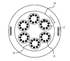
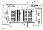
- the coating layer 36 is formed using a film forming apparatus 60 having both a magnetron sputtering cathode and an arc ion plating cathode as shown in the schematic diagram of FIG.
- the method of forming a film is mentioned. That is, a method of forming the lower layer 38 by the magnetron sputtering method and forming the upper layer 39 by the arc ion plating method is preferable.
- the film forming apparatus 60 of FIG. 13 includes a sputtering unit 68 that introduces a gas such as N 2 or Ar into the vacuum chamber 61 from the gas introduction port 62 and includes the cathode electrode 67 and the anode electrode 64.
- a lower layer 38 is formed on the surface of the substrate 35 by sputtering between them.
- the film forming apparatus 60 stops the arc discharge between the cathode electrode 63 and the anode electrode 64 and applies a high voltage between the cathode electrode 63 and the anode electrode 64. Then, plasma is generated, and a desired metal or ceramic is vaporized from the target 65 by the plasma and ionized to be in a high energy state, and the ionized metal is adhered to the surface of the sample (base 35). By continuing the film formation by 66, the upper layer 39 is formed on the surface of the lower layer 38.
- a heater 69 for heating the substrate 35, a gas discharge port 70 for discharging gas out of the system, and a bias power supply 71 for applying a bias voltage to the substrate 35 are arranged. ing. Then, using the target 65, the metal source is evaporated and ionized by arc discharge or glow discharge, and at the same time, nitrogen (N 2 ) gas as a nitrogen source or methane (CH 4 ) / acetylene (C 2 H 2 ) as a carbon source. By reacting with the gas, the coating layer 36 is deposited on the surface of the substrate 35.
- the film forming temperature is set to 500 to 700 ° C., and pulse power of 3 kW to 7 kW is applied to the magnetron sputtering cathode.
- the repetition frequency is set to 20 to 100 kHz, and the duty cycle is set to 5 to 80%.
- a pulse DC voltage of 30 to 150 V, 50 kHz to 350 kHz is applied as a bias voltage, and a discharge state is established by flowing a nitrogen gas of 0.3 to 0.8 Pa, and the lower layer 38 is formed.
- the arc ion plating cathode is irradiated with arc discharge or glow discharge to evaporate and ionize the metal source, and at the same time, nitrogen (N 2 )
- the upper layer 39 is formed on the surface of the lower layer 38 by reacting the gas or the carbon source methane (CH 4 ) / acetylene (C 2 H 2 ) gas at a gas pressure of 2 to 5 Pa.
- the base body 35 is placed on each of the plurality of sample support portions 74 provided on the sample support jig 73 placed on the table 72 so that the rake face faces the target 65.
- a plurality of towers 76 (8 sets of sample support jigs 73 and 2 sets of towers 76 are shown in FIG. 13) are arranged. Note that the sample support jig 73, the tower 76, and the table 72 are rotated, and it is considered that the thickness of the coating layer is uniform with each sample facing the target 65 in order.
- the lower layer 38 and the upper layer 39 are formed by increasing the rotation speed when forming the upper layer 39 at a rate of 1.1 to 3.0 as compared with the rotation speed when forming the lower layer 38.
- the orientation state can be controlled.
- a third embodiment of the cutting tool of the present invention will be described based on an example of a throw-away drill which is a preferred example thereof.
- the basic configuration of the drill according to this embodiment is the same as the drill and the insert shown in the second embodiment described above.
- a coating layer 52 made of a nitride or carbonitride containing Ti and Al and having a layer thickness of 3 to 10 ⁇ m on the cutting edge is coated, Diffraction intensities I (111) and I (200) of the (111), (200), (220), (222), and (400) planes for the X-ray diffraction peak of the Cu—K ⁇ ray in the coating layer 52. , I (220), I (222), I (400) ratio I (220) / (I (111) + I (200) + I (220) + I (222) + I (400)))) q, rake face ( The q value at the upper surface 31 in FIGS.
- q e > q r > q f is desirable for improving the welding resistance at the time of cutting.
- the coating layer 52 is desirably formed by physical vapor deposition (PVD) as in the second embodiment, and in particular, it is formed by arc ion plating so that the hardness and adhesion can be improved. It is more desirable to obtain.
- PVD physical vapor deposition
- film formation is performed while rotating the sample 45 degrees each with the rake face, cutting edge, and flank face during film formation.
- the crystal growth direction of the coating layer 36 can be controlled.
- the variation in the thickness of the entire circumference of the cutting edge of each sample can be reduced, it is difficult to form a portion that tends to be partially lost even if the entire thickness is increased.
- Other steps are the same as those in the second embodiment.
- tungsten carbide (WC) powder having an average particle diameter of 0.8 ⁇ m, 10% by mass of metallic cobalt (Co) powder having an average particle diameter of 1.2 ⁇ m, and vanadium carbide (VC) powder having an average particle diameter of 1.0 ⁇ m.
- Cutting tool shape for milling blade exchangeable milling by press molding 0.2 mass%, chromium carbide (Cr 3 C 2 ) powder with an average particle size of 1.0 ⁇ m added and mixed at a ratio of 0.6 mass%) BDMT11T308ER-JT was debindered and fired at 1450 ° C. for 1 hour in a vacuum of 0.01 Pa to produce a cemented carbide.
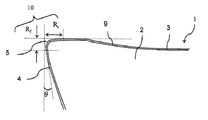
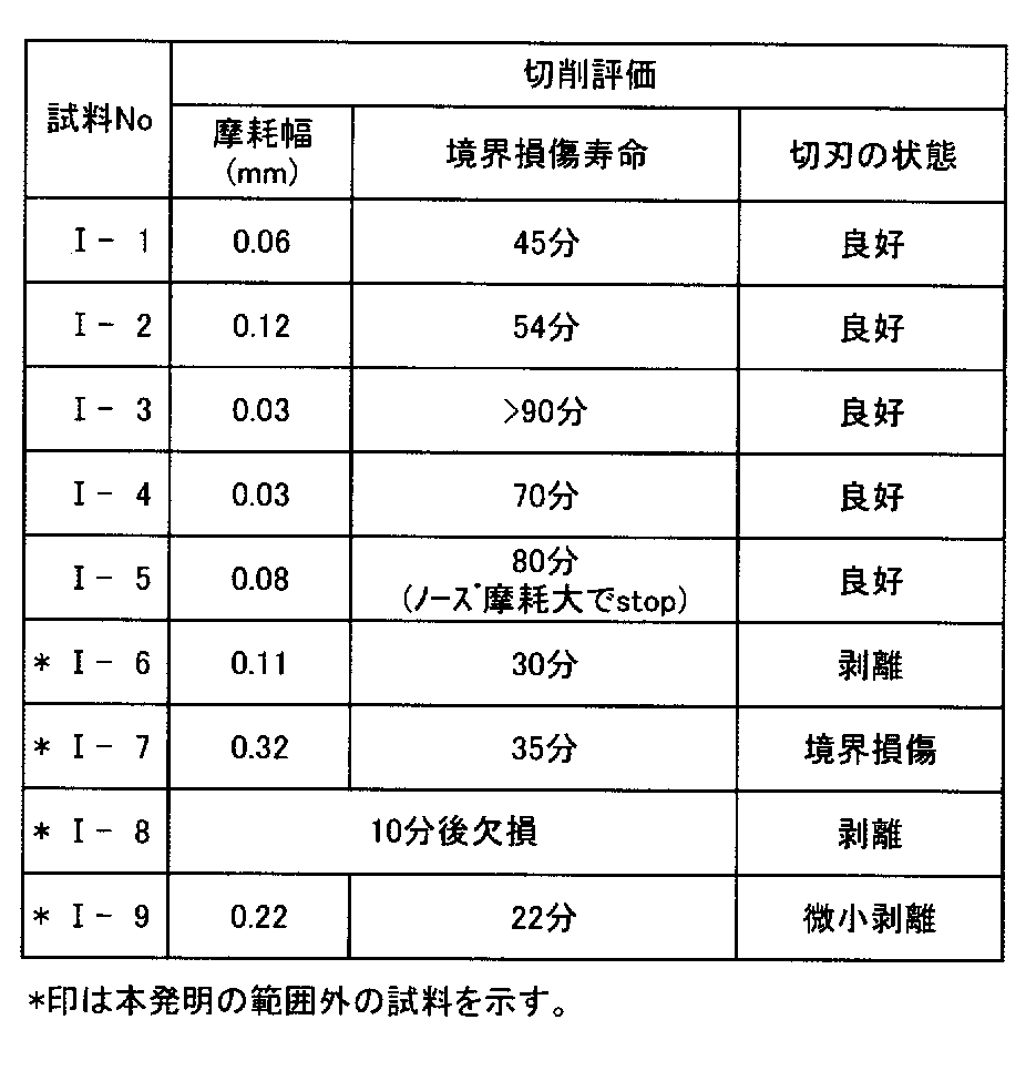
- a coating layer having a TiAlN composition was formed on the substrate thus prepared by sputtering at a film forming temperature of 500 ° C. under the conditions shown in Table 1.
- the rotation speed of the sample shown in Table 1 is a schematic view of the film forming apparatus shown in FIG. 5 as viewed from above. The number of rotations of the tower 16 holding the sample 15 is counted as one rotation and rotated in one minute. The number of rotations made is shown. In FIG. 5, 17 indicates a target, and 18 indicates a sample stage. The layer thickness of the coating layer was measured at the center position of the flank.
- the obtained samples (I-1 to I-9) were subjected to thin film X-ray diffraction analysis, and the peak intensity ratio p of I (400) / I (311) was measured.
- the measurement conditions were an incident angle of 2.0 °, a Cu—K ⁇ ray, Step ⁇ 0.02 °, and Time ⁇ 2 sec.
- p s the surface of the coating layer is not polished and X-rays are irradiated as it is, and thin film X-ray diffraction measurement is performed.
- etching is performed until the layer thickness is within 1.5 ⁇ m (approximately 1 ⁇ m).
- tungsten carbide (WC) powder having an average particle diameter of 1.5 ⁇ m
- 10% by mass of metallic cobalt (Co) powder having an average particle diameter of 1.2 ⁇ m
- 3% by mass of titanium carbide (TiC) powder having an average particle diameter of 1.5 ⁇ m
- a cutting tool shape ZCMT06T204
- debinding treatment fired in a vacuum of 0.01 Pa at 1450 ° C. for 1 hour to produce a cemented carbide.
- the rake face surface of each sample was polished by blasting, brushing or the like.
- the manufactured cemented carbide was subjected to brushing, and a cutting edge treatment (honing) was performed so that the honing amount R was 0.02 ⁇ R ⁇ 0.04 mm.
- a coating layer having various compositions is formed on the substrate thus prepared according to the film formation conditions shown in Table 1 using a film formation apparatus having both a magnetron sputtering cathode and an arc ion plating cathode. Filmed.
- the film formation conditions for the lower layer were as shown in Table 3 by sputtering, with a film formation temperature of 500 ° C., a repetition frequency of 50 kHz, a nitrogen cycle of 75% and 0.3 to 0.8 Pa flowing.
- the upper layer is formed under the conditions shown in Table 1 by introducing nitrogen (N 2 ) gas at a film formation temperature of 550 ° C. and 3.8 Pa into the chamber by the arc ion plating method.
- An insert was prepared.
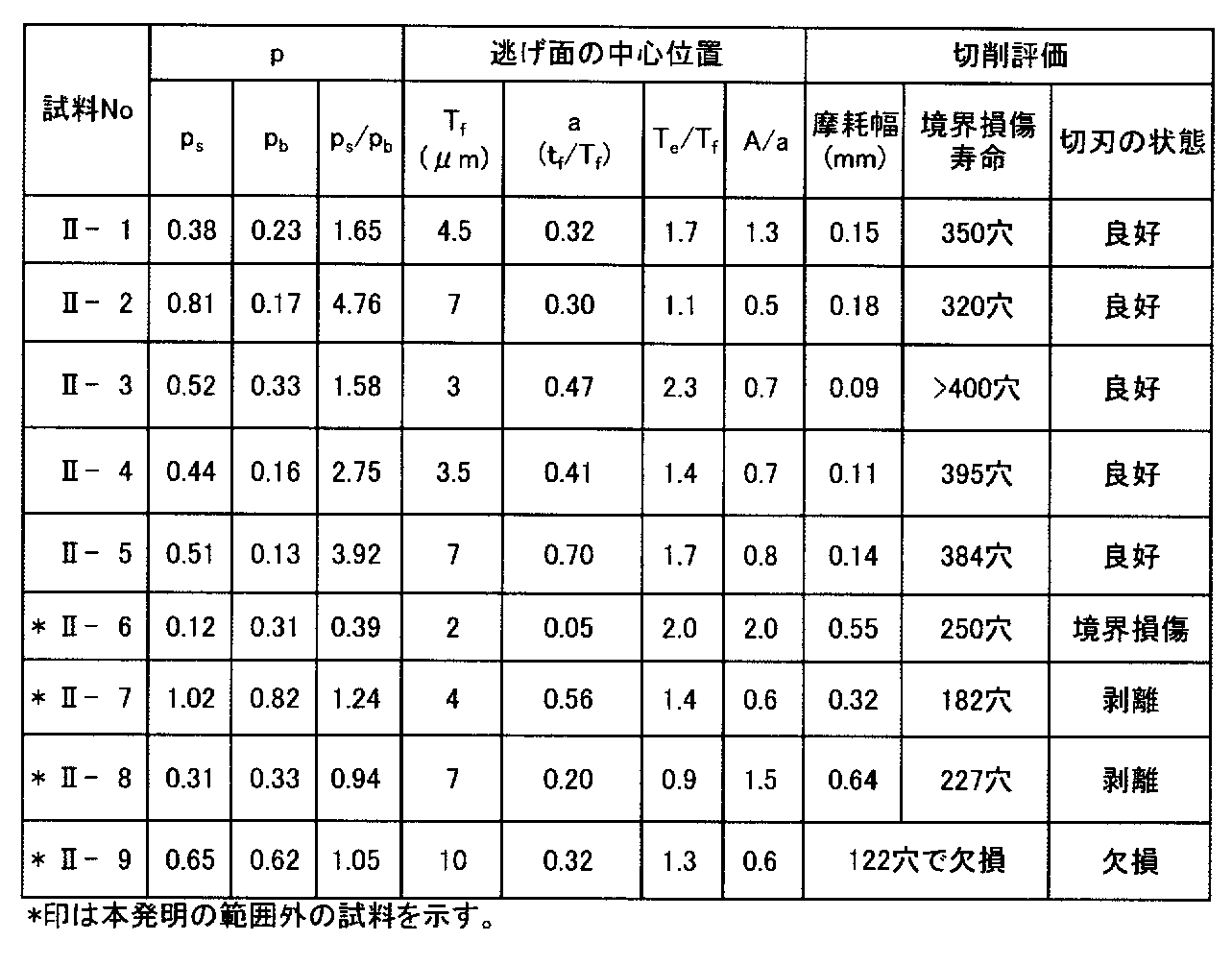
- the rake face and flank face of the obtained samples (II-1 to II-9) were precisely cut so as to be perpendicular to the cutting edge, and the cross-section was observed. From the scanning electron microscope SEM photograph, the coating layer The film thickness was measured. In addition, the film thickness of the coating layer was the thickest at the cutting edge. Further, it was polished obliquely at an angle of 1 ° with respect to the flank, and X-ray diffraction analysis was performed at predetermined positions on the unpolished surface and the polished surface.
- the collimator diameter was 0.3 mm ⁇
- the output was 45 kV, 110 mA
- the incident angle was 2.0 °
- the Cu—K ⁇ line Step ⁇ 0.02 °
- P 1 , P 2 , and P 3 were calculated from diffraction peaks obtained by X-ray diffraction analysis.
- this insert was mounted on the tool main body (Kyocera throw-away drill holder S25-DRZ1734-06) shown in FIG. 6, and the following cutting test was performed to evaluate the cutting performance.
- Cutting method Drilling Work material: Ductile cast iron (FCD450) Cutting speed: 140 m / min Feeding: 0.12mm / tooth Cutting depth: Hole diameter 20mm, hole depth 40mm Cutting state: Wet evaluation method: Cutting was performed with 400 holes as the upper limit, and the number of machining until the inner blade (or outer blade) was damaged was recorded. For the outer blade, the flank wear after 150 holes were measured and the wear resistance was compared. The results are shown in Table 3 or 4.
- the sample No. 1 has the same rotation speed when the lower layer is formed and the rotation speed when the upper layer is formed.
- the P 3 value was larger than the P 1 value and the P 2 value, and the cutting edge was damaged.
- chipping due to peeling of the coating layer occurred.
- the sample No. 1 has a lower rotation speed when forming the upper layer than the rotation speed of the sample when forming the lower layer.
- the P 1 value, the P 2 value, and the P 3 value were P 3 ⁇ P 2 ⁇ P 1 , and the wear width was large and the boundary damage life was also long.
- the sample No. 1 was formed with the rotation speed when the upper layer was formed at a ratio of 1.1 to 3.0 than the rotation speed of the sample when the lower layer was formed.
- P 3 ⁇ P 2 ⁇ P 1 and both the abrasion resistance and the fracture resistance were excellent.
- Example 2 With respect to the substrate manufactured in the same manner as in Example 2, the sample was placed in the film forming apparatus in the state shown in FIG. 7, and nitrogen (N 2 ) gas was introduced into the chamber by the arc ion plating method.
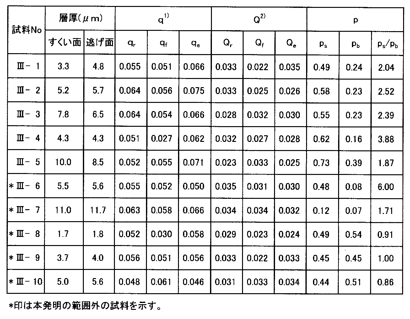
- An insert was manufactured by forming a TiAlN coating layer having a thickness shown in Table 1 by the PVD method under a bias voltage of 35 V (III-1 to III-10).
- Sample No. for III-1 to III-5 the direction of the sample was rotated by 45 ° with respect to the rake face, the cutting edge, and the flank face at an intermediate stage of film formation using a specimen fixing jig.
- the rake face and flank face of the obtained sample were precisely cut so as to be perpendicular to the cutting edge and subjected to cross-sectional observation, and the film thickness of the coating layer was measured from a scanning electron microscope SEM photograph. In addition, the film thickness of the coating layer was the thickest at the cutting edge. Further, a micro X-ray diffraction analysis was performed on the rake face, cutting edge, and flank face. The collimator diameter was 0.3 mm ⁇ , and measurement was performed at the center of the flat portion of each surface. The radiation source was Cu-K ⁇ ray, and the output was 45 kV, 110 mA, incident angle 2.0 °, Cu-K ⁇ ray, Step ⁇ 0.02 °, Time ⁇ 2 sec. From the diffraction peaks obtained by X-ray diffraction analysis, q e , q r , q f , and Q r , Q e , Q f were calculated.
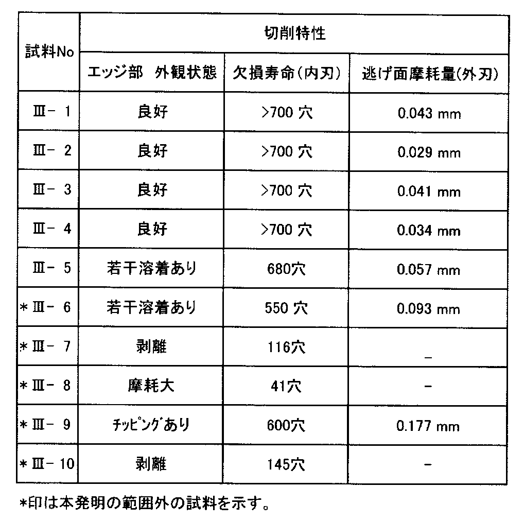
- this insert was mounted on the tool body (Kyocera throw-away drill holder S25-DRZ1734-06) shown in FIG. 1, and the following cutting test was performed to evaluate the cutting performance.
- Cutting method Drilling Work material: Carbon steel (S45C)
- Cutting speed 150 m / min
- Feeding 0.25mm / tooth
- Cutting depth Hole diameter 20mm
- wet evaluation method Cutting was performed with 700 holes as the upper limit, and the number of machining until the inner blade (or outer blade) was damaged was recorded. For the outer cutter, the flank wear after 400 holes were measured and the wear resistance was compared. The results are shown in Table 6.
- the layer thickness of the coating layer in the cutting edge is 3 ⁇ 10 [mu] m, and Sample No. of q e> q r and q e> q f All of III-1 to III-5 were excellent in fracture resistance and wear resistance.
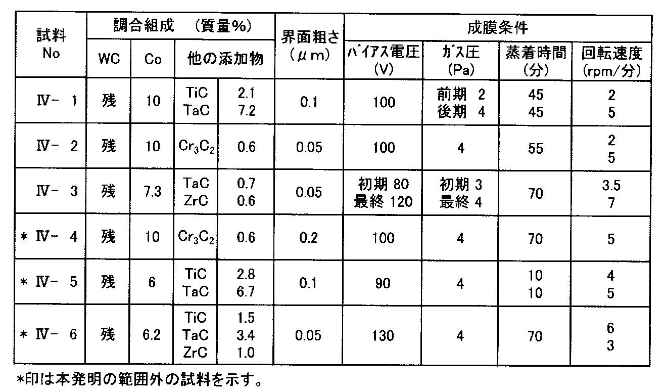
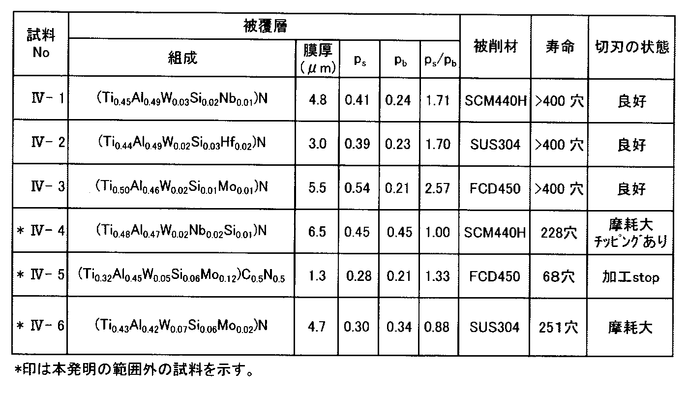
- An insert was prepared by forming a coating layer in the same manner as in Example 3 except that a substrate and a coating layer having the composition shown in Table 7 were used.
- a cutting test was performed using the work material shown in Table 8 under the following conditions. Evaluation was performed in the same manner as in Example 3 (IV-1 to IV-6). The results are shown in Table 8.
- Cutting method Drilling Cutting speed: 120 m / min Feeding: 0.1mm / tooth Cutting depth: Hole diameter 20mm, hole depth 40mm
- Wet evaluation method Cutting was performed with 400 holes as the upper limit, and the number of machining until the inner blade (or outer blade) was damaged was recorded. For the outer cutter, the flank wear after 200 holes was measured and the wear resistance was compared.
- FIG. 3 is a schematic sectional view taken along line aa in FIG.
- FIG. 4 shows a thin film X-ray diffraction pattern for the covering layer of the throw-away chip in FIG.
- FIG. 1 is a schematic view of a film forming apparatus as viewed from above for explaining the arrangement of a film forming apparatus for forming a coating layer of a cutting tool of Example 1 (first embodiment) of a cutting tool of the present invention. . It is a schematic side view which shows the drill concerning 2nd Embodiment of the cutting tool of this invention.
- FIG. 11 is an enlarged view showing a cross section taken along the line II of the insert of FIG. 9, and an enlarged view showing a cross section taken along the line II-II of FIG. FIG.
- FIG. 9 is an enlarged view showing a cross-section of (a) II line of another form (third embodiment) of the insert of FIG. 9 in the drill of the second embodiment, and (b) II-II line. It is an enlarged view which shows a cross section. It is a schematic diagram of the film-forming apparatus which is an example of the film-forming method of the coating layer of the insert of FIG. 11, FIG.
- a Throw-away milling tool (tool) 1 Throw away tip (chip) 2 Substrate 3 Rake face 4 Relief face 5 Corner cutting edge 6 Main cutting edge 7 Sub cutting edge 8 Cutting edge 9 Covering layer 10 Honing R r Honing amount on rake face 3 side R f Honing amount on flank face 4 side 11 Holder 12 Tip Pocket 13 Screw 14 Screw hole 15 Sample 16 Tower 17 Target 18 Sample stand 21 Drill 22 Tool body 23, 53 Throw away insert (insert) 23a One insert 23b The other insert 24 Screw 25 Inner blade 26 Outer blade 28 Shank part 29 Chip discharge groove 30 Insert pocket 30a Inner insert pocket 30b Outer insert pocket 31 Upper surface 32 Side surface 34 Through hole 35 Base body 36, 52 Cover layer 38 Lower layer 39 Upper layer 40 Lower surface (sitting surface) 41 Crossed ridge line portion 42 Inner blade land 43 Inner blade rake surface 44 Inner blade flank surface 45 Outer blade land portion 46 Projection portion 47 Outer blade land 48 Outer blade breaker groove 49 Outer blade rake surface 50 Outer blade flank surface 51 Outer blade rising surface 60 Deposition App
Landscapes
- Chemical & Material Sciences (AREA)
- Engineering & Computer Science (AREA)
- Mechanical Engineering (AREA)
- Chemical Kinetics & Catalysis (AREA)
- Materials Engineering (AREA)
- Metallurgy (AREA)
- Organic Chemistry (AREA)
- Cutting Tools, Boring Holders, And Turrets (AREA)
- Drilling Tools (AREA)
- Physical Vapour Deposition (AREA)
Abstract
Description
本発明の切削工具の一例について、その好適例であるスローアウェイチップ(以下、単にチップと略す。)を装着したスローアウェイ式ミリング工具(以下、単に工具と略す。)Aの先端部についての概略斜視図である図1、装着されるチップ1の(a)概略斜視図、(b)平面図である図2、図2のチップ1について図2(a)のa-aラインについての断面図である図3、図3のチップ1の被覆層9について(s)外表面および(b)基体から1.5μm以内の層厚領域が露出した状態で薄膜X線回折測定したときのX線回折パターンの一例である図4を基に説明する。
次に、上述した第1の切削工具の実施態様についての製造方法の一例について説明する。
本発明の切削工具の第2の実施態様について、その好適例であるスローアウェイドリルの一例を基に説明する。図6は、本実施形態にかかるドリルを示す概略側面図である。図7は、図6のドリルを先端から見た概略正面図である。図8は、図6のドリルを用いて切削した際の外刃と内刃の配置を説明するための模式図である。なお、図8中、破線で示すインサートは、実線で示すインサートが180度回転したときの位置を示している。
そして、焼成後の基体35に被覆層36の成膜方法としてはイオンプレーティング法やスパッタリング法等の物理蒸着(PVD)法が好適に適応可能である。特に、本発明の好適な成膜方法の一例として、図13の模式図に示されるようなマグネトロンスパッタリングカソードとアークイオンプレーティングカソードとの両方を具備する成膜装置60を用いて被覆層36を成膜する方法が挙げられる。つまり、マグネトロンスパッタリング法によって下層38を成膜し、かつアークイオンプレーティング法によって上層39を成膜する方法が好適である。
本発明の切削工具の第3の実施態様について、その好適例であるスローアウェイドリルの一例を基に説明する。本実施形態にかかるドリルの基本的な構成は上述した第2の実施態様に示すドリルおよびインサートと同じ構成である。

切削方法:肩削り(ミリング加工)
被削材 :SKD11
切削速度:150m/min
送り :0.12mm/tooth
切り込み:横切り込み10mm、深さ切り込み3mm
切削状態:湿式
評価方法:15分間切削した時点で、切刃の観察を行うと共に、逃げ面における摩耗量(幅)を測定した。なお、加工済みのホーニング量は摩耗幅には含めないように注意した。
切削方法:穴あけ(ドリル加工)
被削材 :ダクタイル鋳鉄(FCD450)
切削速度:140m/min
送り :0.12mm/tooth
切り込み:穴径20mm、穴深さ40mm
切削状態:湿式
評価方法:400穴加工を上限として切削を行い、内刃(あるいは外刃)に欠損が生じるまでの加工数を記録した。また、外刃については150穴加工後における逃げ面摩耗量を計測し、耐摩耗性の比較も行った。
結果は表3または4に示した。

切削方法:穴あけ(ドリル加工)
被削材 :炭素鋼(S45C)
切削速度:150m/min
送り :0.25mm/tooth
切り込み:穴径20mm、穴深さ20mm
切削状態:湿式
評価方法:700穴加工を上限として切削を行い、内刃(あるいは外刃)に欠損が生じるまでの加工数を記録した。また、外刃については400穴加工後における逃げ面摩耗量を計測し、耐摩耗性の比較も行った。
結果は表6に示した。
切削方法:穴あけ(ドリル加工)
切削速度:120m/min
送り :0.1mm/tooth
切り込み:穴径20mm、穴深さ40mm
切削状態:湿式
評価方法:400穴加工を上限として切削を行い、内刃(あるいは外刃)に欠損が生じるまでの加工数を記録した。また、外刃については200穴加工後における逃げ面摩耗量を計測し、耐摩耗性の比較も行った。
1 スローアウェイチップ(チップ)
2 基体
3 すくい面
4 逃げ面
5 コーナー切刃
6 主切刃
7 副切刃
8 切刃
9 被覆層
10 ホーニング
Rr すくい面3側のホーニング量
Rf 逃げ面4側のホーニング量
11 ホルダ
12 チップポケット
13 ねじ
14 ねじ穴
15 試料
16 タワー
17 ターゲット
18 試料台
21 ドリル
22 工具本体
23、53 スローアウェイインサート(インサート)
23a 一方のインサート
23b 他方のインサート
24 ネジ
25 内刃
26 外刃
28 シャンク部
29 切屑排出溝
30 インサートポケット
30a 内側のインサートポケット
30b 外側のインサートポケット
31 上面
32 側面
34 貫通穴
35 基体
36、52 被覆層
38 下層
39 上層
40 下面(着座面)
41 交差稜線部
42 内刃ランド
43 内刃すくい面
44 内刃逃げ面
45 外刃陸部
46 突出部
47 外刃ランド
48 外刃ブレーカ溝
49 外刃すくい面
50 外刃逃げ面
51 外刃立ち上がり面
60 成膜装置
61 真空チャンバ
62 ガス導入口
63、67 カソード電極
64 アノード電極
65 ターゲット
66 アークイオンプレーティング部
68 スパッタリング部
69 ヒータ
70 ガス排出口
71 バイアス電源
72 テーブル
73 試料支持治具
74 試料支持部
76 タワー
O ドリルの回転軸
L1 下面(着座面)に垂直な線
L2 内刃すくい面の仮想延長線
L3 下面(着座面)に平行な線
L4 外刃すくい面の仮想延長線
L5 外刃立ち上がり面の仮想延長線
α1 内刃すくい角
α2 外刃すくい角
β1 内刃逃げ角
β2 外刃逃げ角
γ 立ち上がり角
Claims (10)
- 基体と、
該基体の表面を被覆するTiとAlとを含む窒化物または炭窒化物からなる被覆層であって、逃げ面における層厚が3~9μmであり、かつCu-Kα線の薄膜X線回折ピークについての(400)面の回折強度I(400)と(311)面の回折強度I(311)との比率I(400)/I(311)をpとするとき、pが前記基体側よりも外表面側で大きい被覆層と、
からなることを特徴とする切削工具。 - 前記被覆層の外表面で薄膜X線回折分析をしたときの前記比率pをpsとするとき、ps=0.2~1であることを特徴とする請求項1記載の切削工具。
- 前記被覆層の前記基体側の界面から厚み1.5μm以内の領域が露出した状態で薄膜X線回折分析をしたときの前記比率pをpbとするとき、pb=0.1~0.5であることを特徴とする請求項1記載の切削工具。
- 前記比率psとpbとの比ps/pbをrとするとき、r=1.5~7であることを特徴とする請求項2または3記載の切削工具。
- 前記被覆層は下層および上層にて構成されており、前記被覆層を厚み方向に対して斜めに研磨した研磨面において該被覆層のCu-Kα線のX線回折ピークについての(400)面の回折強度I(400)と(311)面の回折強度I(311)との比率I(400)/I(311)をPとするとき、前記被覆層の未研磨面で測定したP1=0.1~0.5であるとともに、前記研磨面の前記下層と前記上層との界面が露出した部分で測定したP3が前記研磨面のうちの上層が残存する部分で測定したP2よりも小さく、かつ該P2が前記P1よりも小さいことを特徴とする請求項1乃至3のいずれか記載の切削工具。
- 前記被覆層の前記切刃における総厚みTeが3~15μmであり、前記逃げ面の中心位置における前記被覆層の厚みTfに対する比(Te/Tf)が1.2~3.8であることを特徴とする請求項5記載の切削工具。
- 前記切刃における前記被覆層の総厚みTeに対する前記下層の厚みteの比率(te/Te)をAとするとき、比率Aが0.2~0.6であるとともに、前記逃げ面の中心位置における前記被覆層の総厚みTfに対する前記下層の厚みtfの比率(tf/Tf)をaとするとき、比率aに対する比率Aの比(A/a)が0.4~0.9であることを特徴とする請求項6記載の切削工具。
- 前記被覆層の切刃における層厚が3~10μmであり、かつ前記被覆層のCu-Kα線の微小部X線回折ピークについての(111)、(200)、(220)、(222)、(400)面それぞれの回折強度I(111)、I(200)、I(220)、I(222)、I(400)に関する比率I(220)/(I(111)+I(200)+I(220)+I(222)+I(400))をq、すくい面におけるq値をqr、逃げ面におけるq値をqf、切刃におけるq値をqeとしたとき、qe>qrかつqe>qfであることを特徴とする請求項1乃至7のいずれか記載の切削工具。
- qe>qr>qfであることを特徴とする請求項8記載の切削工具。
- 前記被覆層の(111)、(200)、(220)、(222)、(400)面それぞれの回折強度I(111)、I(200)、I(220)、I(222)、I(400)に関する比率I(400)/(I(111)+I(200)+I(220)+I(222)+I(400))をQ、すくい面におけるQ値をQr、逃げ面におけるQ値をQf、切刃におけるQ値をQeとしたとき、Qr>Qe>Qfであることを特徴とする請求項8または9記載の切削工具。
Priority Applications (4)
| Application Number | Priority Date | Filing Date | Title |
|---|---|---|---|
| EP09705353.2A EP2243578B1 (en) | 2008-01-29 | 2009-01-29 | Cutting tool |
| JP2009551570A JP5116777B2 (ja) | 2008-01-29 | 2009-01-29 | 切削工具 |
| US12/863,239 US8415033B2 (en) | 2008-01-29 | 2009-01-29 | Cutting tool |
| CN2009801025785A CN101952070B (zh) | 2008-01-29 | 2009-01-29 | 切削工具 |
Applications Claiming Priority (6)
| Application Number | Priority Date | Filing Date | Title |
|---|---|---|---|
| JP2008-017105 | 2008-01-29 | ||
| JP2008017105 | 2008-01-29 | ||
| JP2008-167413 | 2008-06-26 | ||
| JP2008167413 | 2008-06-26 | ||
| JP2008-219246 | 2008-08-28 | ||
| JP2008219246 | 2008-08-28 |
Publications (1)
| Publication Number | Publication Date |
|---|---|
| WO2009096476A1 true WO2009096476A1 (ja) | 2009-08-06 |
Family
ID=40912820
Family Applications (1)
| Application Number | Title | Priority Date | Filing Date |
|---|---|---|---|
| PCT/JP2009/051483 Ceased WO2009096476A1 (ja) | 2008-01-29 | 2009-01-29 | 切削工具 |
Country Status (5)
| Country | Link |
|---|---|
| US (1) | US8415033B2 (ja) |
| EP (1) | EP2243578B1 (ja) |
| JP (1) | JP5116777B2 (ja) |
| CN (1) | CN101952070B (ja) |
| WO (1) | WO2009096476A1 (ja) |
Cited By (6)
| Publication number | Priority date | Publication date | Assignee | Title |
|---|---|---|---|---|
| CN101837475A (zh) * | 2010-04-28 | 2010-09-22 | 株洲钻石切削刀具股份有限公司 | 加工铝材用涂层刀片及其制备方法 |
| JP2012101336A (ja) * | 2010-11-12 | 2012-05-31 | Mitsubishi Materials Corp | 耐摩耗性と切屑排出性に優れた表面被覆ドリル |
| WO2015093530A1 (ja) * | 2013-12-17 | 2015-06-25 | 京セラ株式会社 | 被覆工具 |
| JP2019025570A (ja) * | 2017-07-27 | 2019-02-21 | 株式会社タンガロイ | エンドミル |
| JP2019111631A (ja) * | 2017-12-26 | 2019-07-11 | 三菱日立ツール株式会社 | 被覆切削工具 |
| JP2020157378A (ja) * | 2019-03-25 | 2020-10-01 | 株式会社Moldino | 被覆工具 |
Families Citing this family (23)
| Publication number | Priority date | Publication date | Assignee | Title |
|---|---|---|---|---|
| US8080071B1 (en) | 2008-03-03 | 2011-12-20 | Us Synthetic Corporation | Polycrystalline diamond compact, methods of fabricating same, and applications therefor |
| US8236074B1 (en) | 2006-10-10 | 2012-08-07 | Us Synthetic Corporation | Superabrasive elements, methods of manufacturing, and drill bits including same |
| US9017438B1 (en) | 2006-10-10 | 2015-04-28 | Us Synthetic Corporation | Polycrystalline diamond compact including a polycrystalline diamond table with a thermally-stable region having at least one low-carbon-solubility material and applications therefor |
| US8821604B2 (en) * | 2006-11-20 | 2014-09-02 | Us Synthetic Corporation | Polycrystalline diamond compact and method of making same |
| US8034136B2 (en) | 2006-11-20 | 2011-10-11 | Us Synthetic Corporation | Methods of fabricating superabrasive articles |
| US8080074B2 (en) | 2006-11-20 | 2011-12-20 | Us Synthetic Corporation | Polycrystalline diamond compacts, and related methods and applications |
| US8911521B1 (en) | 2008-03-03 | 2014-12-16 | Us Synthetic Corporation | Methods of fabricating a polycrystalline diamond body with a sintering aid/infiltrant at least saturated with non-diamond carbon and resultant products such as compacts |
| US8999025B1 (en) | 2008-03-03 | 2015-04-07 | Us Synthetic Corporation | Methods of fabricating a polycrystalline diamond body with a sintering aid/infiltrant at least saturated with non-diamond carbon and resultant products such as compacts |
| US8071173B1 (en) | 2009-01-30 | 2011-12-06 | Us Synthetic Corporation | Methods of fabricating a polycrystalline diamond compact including a pre-sintered polycrystalline diamond table having a thermally-stable region |
| US10309158B2 (en) | 2010-12-07 | 2019-06-04 | Us Synthetic Corporation | Method of partially infiltrating an at least partially leached polycrystalline diamond table and resultant polycrystalline diamond compacts |
| US9027675B1 (en) | 2011-02-15 | 2015-05-12 | Us Synthetic Corporation | Polycrystalline diamond compact including a polycrystalline diamond table containing aluminum carbide therein and applications therefor |
| US9555476B2 (en) * | 2013-02-22 | 2017-01-31 | Kyocera Corporation | Cutting tool |
| KR101704629B1 (ko) * | 2013-09-11 | 2017-02-08 | 미츠비시 히타치 쓰루 가부시키가이샤 | 날끝 교환식 회전 절삭 공구 |
| JP6390706B2 (ja) | 2014-08-01 | 2018-09-19 | 株式会社タンガロイ | 被覆切削工具 |
| US10570501B2 (en) | 2017-05-31 | 2020-02-25 | Kennametal Inc. | Multilayer nitride hard coatings |
| CN107363706B (zh) * | 2017-08-30 | 2023-06-27 | 浙江工业大学 | 一种可旋转珩磨夹具 |
| CN109570629B (zh) * | 2017-09-28 | 2020-09-25 | 株式会社泰珂洛 | 切削工具 |
| US12194542B2 (en) | 2019-03-27 | 2025-01-14 | Kyocera Corporation | Coated tool and cutting tool including same |
| JP7128351B2 (ja) * | 2019-04-22 | 2022-08-30 | 京セラ株式会社 | インサート及びこれを備えた切削工具 |
| JP7308938B2 (ja) | 2019-05-29 | 2023-07-14 | 京セラ株式会社 | 被覆工具および切削工具 |
| CN116367944B (zh) * | 2020-10-21 | 2025-06-06 | 京瓷株式会社 | 金属陶瓷制刀片以及具备该金属陶瓷制刀片的切削刀具 |
| US20240309514A1 (en) * | 2021-04-30 | 2024-09-19 | Sumitomo Electric Industries, Ltd. | Cutting tool |
| JP7760424B2 (ja) * | 2022-03-22 | 2025-10-27 | 株式会社神戸製鋼所 | 被覆部材 |
Citations (5)
| Publication number | Priority date | Publication date | Assignee | Title |
|---|---|---|---|---|
| JPH09295204A (ja) | 1996-04-26 | 1997-11-18 | Hitachi Tool Eng Ltd | 表面被覆スローアウェイインサート |
| JPH09300106A (ja) | 1996-05-21 | 1997-11-25 | Hitachi Tool Eng Ltd | 表面被覆超硬合金製スローアウェイインサート |
| JPH10330914A (ja) | 1997-05-28 | 1998-12-15 | Toshiba Tungaloy Co Ltd | 結晶配向性硬質膜を含む積層被膜部材 |
| JP2002003284A (ja) | 2000-06-14 | 2002-01-09 | Toshiba Tungaloy Co Ltd | 硬質膜被覆超高温高圧焼結体 |
| JP2006316351A (ja) * | 2000-12-28 | 2006-11-24 | Kobe Steel Ltd | 切削工具用硬質皮膜の製造方法 |
Family Cites Families (8)
| Publication number | Priority date | Publication date | Assignee | Title |
|---|---|---|---|---|
| DE69431032T2 (de) * | 1993-05-31 | 2003-01-30 | Sumitomo Electric Industries, Ltd. | Beschichtetes schneidwerkzeug und verfahren zu dessen herstellung |
| EP1992717B1 (en) * | 2000-12-28 | 2012-02-15 | Kabushiki Kaisha Kobe Seiko Sho | Use of a target for arc ion plating to form a hard film |
| US7150925B2 (en) * | 2001-10-30 | 2006-12-19 | Mitsubishi Materials Kobe Tools Corporation | Surface coated cemented carbide cutting tool having hard coating layer exhibiting excellent wear resistance in high speed machining |
| JP4022865B2 (ja) * | 2002-09-27 | 2007-12-19 | 住友電工ハードメタル株式会社 | 被覆切削工具 |
| SE527346C2 (sv) * | 2003-04-24 | 2006-02-14 | Seco Tools Ab | Skär med beläggning av skikt av MTCVD-Ti (C,N) med styrd kornstorlek och morfologi och metod för att belägga skäret |
| CA2531028C (en) * | 2003-06-27 | 2009-07-14 | Sumitomo Electric Industries, Ltd. | Surface-coated high hardness material for tool |
| US7789598B2 (en) * | 2005-07-12 | 2010-09-07 | Kyocera Corporation | Surface coated cutting tool |
| JP2009120912A (ja) * | 2007-11-15 | 2009-06-04 | Kobe Steel Ltd | 硬質皮膜を備えた耐摩耗性部材 |
-
2009
- 2009-01-29 CN CN2009801025785A patent/CN101952070B/zh not_active Expired - Fee Related
- 2009-01-29 EP EP09705353.2A patent/EP2243578B1/en not_active Not-in-force
- 2009-01-29 JP JP2009551570A patent/JP5116777B2/ja not_active Expired - Fee Related
- 2009-01-29 WO PCT/JP2009/051483 patent/WO2009096476A1/ja not_active Ceased
- 2009-01-29 US US12/863,239 patent/US8415033B2/en not_active Expired - Fee Related
Patent Citations (5)
| Publication number | Priority date | Publication date | Assignee | Title |
|---|---|---|---|---|
| JPH09295204A (ja) | 1996-04-26 | 1997-11-18 | Hitachi Tool Eng Ltd | 表面被覆スローアウェイインサート |
| JPH09300106A (ja) | 1996-05-21 | 1997-11-25 | Hitachi Tool Eng Ltd | 表面被覆超硬合金製スローアウェイインサート |
| JPH10330914A (ja) | 1997-05-28 | 1998-12-15 | Toshiba Tungaloy Co Ltd | 結晶配向性硬質膜を含む積層被膜部材 |
| JP2002003284A (ja) | 2000-06-14 | 2002-01-09 | Toshiba Tungaloy Co Ltd | 硬質膜被覆超高温高圧焼結体 |
| JP2006316351A (ja) * | 2000-12-28 | 2006-11-24 | Kobe Steel Ltd | 切削工具用硬質皮膜の製造方法 |
Non-Patent Citations (1)
| Title |
|---|
| See also references of EP2243578A4 |
Cited By (9)
| Publication number | Priority date | Publication date | Assignee | Title |
|---|---|---|---|---|
| CN101837475A (zh) * | 2010-04-28 | 2010-09-22 | 株洲钻石切削刀具股份有限公司 | 加工铝材用涂层刀片及其制备方法 |
| JP2012101336A (ja) * | 2010-11-12 | 2012-05-31 | Mitsubishi Materials Corp | 耐摩耗性と切屑排出性に優れた表面被覆ドリル |
| WO2015093530A1 (ja) * | 2013-12-17 | 2015-06-25 | 京セラ株式会社 | 被覆工具 |
| JP5890594B2 (ja) * | 2013-12-17 | 2016-03-22 | 京セラ株式会社 | 被覆工具 |
| US10174421B2 (en) | 2013-12-17 | 2019-01-08 | Kyocera Corporation | Coated tool |
| JP2019025570A (ja) * | 2017-07-27 | 2019-02-21 | 株式会社タンガロイ | エンドミル |
| JP2019111631A (ja) * | 2017-12-26 | 2019-07-11 | 三菱日立ツール株式会社 | 被覆切削工具 |
| JP2020157378A (ja) * | 2019-03-25 | 2020-10-01 | 株式会社Moldino | 被覆工具 |
| JP7247452B2 (ja) | 2019-03-25 | 2023-03-29 | 株式会社Moldino | 被覆工具 |
Also Published As
| Publication number | Publication date |
|---|---|
| CN101952070A (zh) | 2011-01-19 |
| JP5116777B2 (ja) | 2013-01-09 |
| US20110058909A1 (en) | 2011-03-10 |
| CN101952070B (zh) | 2013-03-13 |
| JPWO2009096476A1 (ja) | 2011-05-26 |
| EP2243578A4 (en) | 2012-06-06 |
| EP2243578B1 (en) | 2015-03-11 |
| US8415033B2 (en) | 2013-04-09 |
| EP2243578A1 (en) | 2010-10-27 |
Similar Documents
| Publication | Publication Date | Title |
|---|---|---|
| JP5116777B2 (ja) | 切削工具 | |
| EP2623241B1 (en) | Cutting tool | |
| JP5542925B2 (ja) | 切削工具 | |
| JP4975193B2 (ja) | 切削工具 | |
| JP5883161B2 (ja) | 切削工具 | |
| WO2013015302A1 (ja) | 切削工具 | |
| JP4991361B2 (ja) | 回転工具 | |
| US8900336B2 (en) | Cutting tool | |
| JP2009285760A (ja) | 切削工具 | |
| JP5517577B2 (ja) | 溝入れ加工用切削工具 | |
| JP5404232B2 (ja) | 切削工具 | |
| JP5247377B2 (ja) | 切削工具 | |
| JP5922546B2 (ja) | 切削工具 | |
| WO2020039736A1 (ja) | 切削工具 | |
| JP5495735B2 (ja) | 切削工具 | |
| JP5334704B2 (ja) | 切削工具 | |
| JP5686254B2 (ja) | 表面被覆切削工具 | |
| JP5219618B2 (ja) | 切削工具 | |
| JP3972294B2 (ja) | 高速切削加工で硬質被覆層がすぐれた耐摩耗性を発揮する表面被覆超硬合金製切削工具 | |
| WO2024190288A1 (ja) | 被覆工具及び切削工具 | |
| JP2021154460A (ja) | 表面被覆切削工具 | |
| JP5713663B2 (ja) | 切削工具 | |
| JP2011093019A (ja) | 切削工具 |
Legal Events
| Date | Code | Title | Description |
|---|---|---|---|
| WWE | Wipo information: entry into national phase |
Ref document number: 200980102578.5 Country of ref document: CN |
|
| 121 | Ep: the epo has been informed by wipo that ep was designated in this application |
Ref document number: 09705353 Country of ref document: EP Kind code of ref document: A1 |
|
| WWE | Wipo information: entry into national phase |
Ref document number: 12863239 Country of ref document: US |
|
| WWE | Wipo information: entry into national phase |
Ref document number: 2009551570 Country of ref document: JP |
|
| NENP | Non-entry into the national phase |
Ref country code: DE |
|
| WWE | Wipo information: entry into national phase |
Ref document number: 2009705353 Country of ref document: EP |