WO2009098857A1 - 色素増感太陽電池 - Google Patents
色素増感太陽電池 Download PDFInfo
- Publication number
- WO2009098857A1 WO2009098857A1 PCT/JP2009/000389 JP2009000389W WO2009098857A1 WO 2009098857 A1 WO2009098857 A1 WO 2009098857A1 JP 2009000389 W JP2009000389 W JP 2009000389W WO 2009098857 A1 WO2009098857 A1 WO 2009098857A1
- Authority
- WO
- WIPO (PCT)
- Prior art keywords
- electrode substrate
- wiring
- dye
- solar cell
- film
- Prior art date
- Legal status (The legal status is an assumption and is not a legal conclusion. Google has not performed a legal analysis and makes no representation as to the accuracy of the status listed.)
- Ceased
Links
Images


Classifications
-
- H—ELECTRICITY
- H01—ELECTRIC ELEMENTS
- H01G—CAPACITORS; CAPACITORS, RECTIFIERS, DETECTORS, SWITCHING DEVICES, LIGHT-SENSITIVE OR TEMPERATURE-SENSITIVE DEVICES OF THE ELECTROLYTIC TYPE
- H01G9/00—Electrolytic capacitors, rectifiers, detectors, switching devices, light-sensitive or temperature-sensitive devices; Processes of their manufacture
- H01G9/20—Light-sensitive devices
- H01G9/2027—Light-sensitive devices comprising an oxide semiconductor electrode
- H01G9/2031—Light-sensitive devices comprising an oxide semiconductor electrode comprising titanium oxide, e.g. TiO2
-
- H—ELECTRICITY
- H01—ELECTRIC ELEMENTS
- H01G—CAPACITORS; CAPACITORS, RECTIFIERS, DETECTORS, SWITCHING DEVICES, LIGHT-SENSITIVE OR TEMPERATURE-SENSITIVE DEVICES OF THE ELECTROLYTIC TYPE
- H01G9/00—Electrolytic capacitors, rectifiers, detectors, switching devices, light-sensitive or temperature-sensitive devices; Processes of their manufacture
- H01G9/20—Light-sensitive devices
- H01G9/209—Light trapping arrangements
-
- H—ELECTRICITY
- H01—ELECTRIC ELEMENTS
- H01G—CAPACITORS; CAPACITORS, RECTIFIERS, DETECTORS, SWITCHING DEVICES, LIGHT-SENSITIVE OR TEMPERATURE-SENSITIVE DEVICES OF THE ELECTROLYTIC TYPE
- H01G9/00—Electrolytic capacitors, rectifiers, detectors, switching devices, light-sensitive or temperature-sensitive devices; Processes of their manufacture
- H01G9/20—Light-sensitive devices
- H01G9/2059—Light-sensitive devices comprising an organic dye as the active light absorbing material, e.g. adsorbed on an electrode or dissolved in solution
-
- H—ELECTRICITY
- H10—SEMICONDUCTOR DEVICES; ELECTRIC SOLID-STATE DEVICES NOT OTHERWISE PROVIDED FOR
- H10K—ORGANIC ELECTRIC SOLID-STATE DEVICES
- H10K30/00—Organic devices sensitive to infrared radiation, light, electromagnetic radiation of shorter wavelength or corpuscular radiation
- H10K30/80—Constructional details
- H10K30/81—Electrodes
- H10K30/82—Transparent electrodes, e.g. indium tin oxide [ITO] electrodes
- H10K30/83—Transparent electrodes, e.g. indium tin oxide [ITO] electrodes comprising arrangements for extracting the current from the cell, e.g. metal finger grid systems to reduce the serial resistance of transparent electrodes
-
- Y—GENERAL TAGGING OF NEW TECHNOLOGICAL DEVELOPMENTS; GENERAL TAGGING OF CROSS-SECTIONAL TECHNOLOGIES SPANNING OVER SEVERAL SECTIONS OF THE IPC; TECHNICAL SUBJECTS COVERED BY FORMER USPC CROSS-REFERENCE ART COLLECTIONS [XRACs] AND DIGESTS
- Y02—TECHNOLOGIES OR APPLICATIONS FOR MITIGATION OR ADAPTATION AGAINST CLIMATE CHANGE
- Y02E—REDUCTION OF GREENHOUSE GAS [GHG] EMISSIONS, RELATED TO ENERGY GENERATION, TRANSMISSION OR DISTRIBUTION
- Y02E10/00—Energy generation through renewable energy sources
- Y02E10/50—Photovoltaic [PV] energy
- Y02E10/542—Dye sensitized solar cells
Definitions
- the present invention relates to a dye-sensitized solar cell having a wiring portion adjacent to a porous oxide semiconductor layer.
- Dye-sensitized solar cells use an electrolyte that corrodes metals. For this reason, when providing the current collection wiring for reducing the current collection resistance of a cell, the wiring protective layer which protects current collection wiring from electrolyte solution is needed. However, when the wiring protective layer is applied to both sides of the current collecting wiring, the thickness of the wiring protective layer is added to the wiring width and the width of the entire wiring tends to increase.
- the wiring of the dye-sensitized solar cell is often formed of a silver paste using a low-melting glass as a binder, and the low-melting glass is often dark. For this reason, the color of the surface after wiring formation becomes dark, and light incident on the wiring portion is absorbed.
- Many of the materials used for the wiring protective layer are transparent or dark, and light is absorbed by the dark-colored wiring protective layer or the dark electrolyte solution behind the transparent wiring protective layer.
- Non-Patent Document 1 introduces a prismatic cover.
- Patent Documents 1 and 2 describe a method using a condensing lens array.
- Patent Document 3 when light incident between solar cell elements in a solar cell module is passed through the back surface of the solar cell module and used for daylighting, the solar cell module is arranged between solar cell elements in order to make the illuminance of the transmitted light uniform.
- a lens is formed on the transparent part of the sheet.
- Patent Document 4 discloses a dye-sensitized solar cell in which a phosphor is disposed on a transparent substrate of a dye-sensitized solar cell, and a part of incident light is converted into light having a wavelength with high photoelectric conversion quantum efficiency, thereby improving power generation efficiency.
- Non-Patent Document 1 and Patent Documents 1 and 2 have a large cost for the lens array and the cover and must be designed exclusively. For this reason, it could not be easily applied in accordance with various cell shapes. Such a decrease in the degree of freedom in design impairs the merits of dye-sensitized solar cells that can be manufactured in various quantities by changing the color and shape to various designs.
- the solar cell module of Patent Document 3 uses light transmitted through a lens for daylighting on the back side of the module, and is not used for power generation by a solar cell element.
- the dye-sensitized solar cell of Patent Document 4 improves the power generation efficiency against light absorption by the high-concentration iodine electrolyte, but does not disclose any special measures for the metal wiring layer.
- an object of the present invention is to provide a dye-sensitized solar cell capable of improving power generation efficiency by suppressing light absorption by a wiring portion.
- the present invention provides a first electrode substrate comprising a porous oxide semiconductor layer carrying a dye and a wiring portion provided in a portion adjacent to the porous oxide semiconductor layer on one side.
- a second electrode substrate disposed to face the porous oxide semiconductor layer of the first electrode substrate, and at least a part between the first electrode substrate and the second electrode substrate At least one of the first electrode substrate, the wiring portion, and the second electrode substrate at a position corresponding to the current collector wiring.
- a dye-sensitized solar cell characterized in that an incident light direction changing unit for changing the direction is provided.
- the direction of light incident on the wiring portion that is the non-power generation portion is changed to the porous oxide semiconductor layer that supports the dye that is the power generation portion by the incident light direction changing portion. It can be changed to head.
- the incident light direction changing unit may be a film body, for example.
- the film body may be, for example, any one of a diffusion film, a diffraction grating film, a fluorescent paint film, and a reflection film.
- the incident light direction changing portion is on a line connecting the first electrode substrate, the wiring portion, and the second electrode substrate, and along the thickness direction of the first electrode substrate or the second electrode substrate. It is preferable that it is provided on the line.
- the first electrode substrate is a transparent electrode substrate, and the incident light direction changing portion is provided on the opposite side of the wiring portion with respect to the first electrode substrate.
- the first electrode substrate is a transparent electrode substrate
- the wiring portion includes a current collecting wiring and a wiring protective layer provided so as to cover the current collecting wiring.
- the wiring protective layer may have a configuration having the incident light direction changing portion.
- the first electrode substrate is a transparent electrode substrate
- the wiring portion includes a current collecting wiring and a wiring protective layer provided so as to cover the current collecting wiring.
- the said incident light direction change part may have the structure provided between the said current collection wiring and the said 1st electrode substrate.
- the second electrode substrate is a transparent electrode substrate, and the incident light direction changing portion is opposite to the first electrode substrate with respect to the second electrode substrate. You may have the structure provided.
- the second electrode substrate is a transparent electrode substrate
- the wiring portion includes a current collecting wiring and a wiring protective layer provided so as to cover the current collecting wiring.
- the wiring protective layer may have a configuration having the incident light direction changing portion.
- the film body is preferably arranged in a range that is larger than the width of the wiring portion and does not overlap with the adjacent porous oxide semiconductor layer.
- the direction of light incident toward the wiring portion that is a non-power generation portion is changed by the incident light direction changing portion so as to be directed to the porous oxide semiconductor layer that supports the dye that is the power generation portion. Therefore, the power generation efficiency can be improved.
- L incident light
- S light whose direction is changed by the film body
- R re-reflected light on the substrate surface
- 10, 20, 30, 40 dye-sensitized solar cell, 11, 21, 31, 41 ... transparent electrode
- FIG. 1 is a cross-sectional view showing a first example of the dye-sensitized solar cell of the present invention.
- FIG. 2 is a cross-sectional view showing a second example of the dye-sensitized solar cell of the present invention.
- FIG. 3 is a cross-sectional view showing a third example of the dye-sensitized solar cell of the present invention.
- FIG. 4 is a cross-sectional view showing a fourth example of the dye-sensitized solar cell of the present invention.
- FIG. 5 is a cross-sectional view showing a fifth example of the dye-sensitized solar cell of the present invention.
- FIG. 6 is a plan view for explaining the arrangement of current collecting wiring between a plurality of cells.
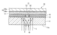
- a dye-sensitized solar cell 10 shown in FIG. 1 includes a first electrode substrate 11, a transparent conductive film 12 formed on the first electrode substrate 11, and a wiring portion 19 formed on the transparent conductive film 12.
- the porous oxide semiconductor layer 15 provided adjacent to the wiring portion 19 on the transparent conductive film 12 and the second oxide oxide layer 15 disposed so as to face the porous oxide semiconductor layer 15 of the first electrode substrate 11.
- Electrode substrate 16 and an electrolyte layer 17 disposed between both electrode substrates 11 and 16.
- the wiring part 19 includes a current collecting wiring 13 formed on the transparent conductive film 12 and a wiring protective layer 14 formed so as to cover the current collecting wiring 13.
- the first electrode substrate 11, which is a transparent electrode substrate includes a film body 18 that changes the direction of incident light at a position corresponding to the wiring portion 19.
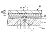
- a dye-sensitized solar cell 20 shown in FIG. 2 includes a first electrode substrate 21, a transparent conductive film 22 formed on the first electrode substrate 21, and a wiring portion 29 formed on the transparent conductive film 22.
- the porous oxide semiconductor layer 25 provided adjacent to the wiring portion 29 on the transparent conductive film 22 and the second oxide oxide layer 25 disposed so as to face the porous oxide semiconductor layer 25 of the first electrode substrate 21.
- Electrode substrate 26 and an electrolyte layer 27 disposed between the electrode substrates 21 and 26.
- the wiring portion 29 includes a current collecting wiring 23 formed on the transparent conductive film 22 and a wiring protective layer 24 formed so as to cover the current collecting wiring 23.
- the wiring protective layer 24 is disposed at a position corresponding to the wiring portion 29 and has a function of changing the direction of incident light.
- the wiring protection layer 24 also serves as a film body that is disposed at a position corresponding to the wiring portion 29 and changes the direction of incident light.
- the film body 24 is provided in the wiring portion 29.
- the dye-sensitized solar cell 30 shown in FIG. 3 is adjacent to the first electrode substrate 36, the wiring portion 39 formed on the first electrode substrate 36, and the wiring portion 39 on the first electrode substrate 36.
- the transparent conductive film 32 formed on the electrode substrate 31 and the electrolyte layer 37 disposed between the electrode substrates 31 and 36 are provided.
- the wiring part 39 includes a current collecting wiring 33 formed on the first electrode substrate 36 and a wiring protective layer 34 formed so as to cover the current collecting wiring 33.
- the second electrode substrate 31, which is a transparent electrode substrate, includes a film body 38 that changes the direction of incident light at a position corresponding to the wiring portion 33.
- the film bodies 18, 24, 38, 44 that change the direction of incident light are provided at positions corresponding to the wiring portions 19, 29, 39, 49. That is, if the film bodies 18, 24, 38, 44 are not present, incident light that is incident on the current collecting wirings 13, 23, 33, 43 or the wiring protective layers 14, 24, 34, 44 and absorbed is absorbed by the film bodies. 18, 24, 38 and 44.
- the light incident on the film bodies 18, 24, 38, 44 is redirected by the film bodies 18, 24, 38, 44, and at least a part of the porous oxide semiconductor layer 15, which is a power generation part, 25, 35, 45. Thereby, the energy loss of incident light can be suppressed and the power generation efficiency can be improved.
- the first electrode substrate 11 provided with the porous oxide semiconductor layer 15 is a transparent electrode substrate, and the incident light L is the first electrode substrate. 11 is incident.
- a film body 18 that changes the direction of the incident light L is provided.
- the film body 18 a diffusion film, a diffraction grating film, or a fluorescent paint film can be used. In this case, the light S in which the direction of the incident light L is changed by the film body 18 can be incident on the porous oxide semiconductor layer 15.
- the first electrode substrate 21 provided with the porous oxide semiconductor layer 25 is a transparent electrode substrate, and the incident light L is the first electrode substrate. 21 is incident.
- the wiring protective layer 24 provided on the surface of the current collecting wiring 23 also serves as the film body 24 that changes the direction of the incident light L.
- a reflection film that increases the reflectance of the wiring surface can be used. In this case, the light S reflected by the wiring protective layer 24 including the reflective film is reflected again by the surface 21 a of the first electrode substrate 21, and the reflected light R can be incident on the porous oxide semiconductor layer 25.
- the light incident on the film body 24 can also enter the porous oxide semiconductor layer 25 through the electrolyte layer 27.
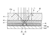
- the current collecting wiring 23 made of the conductive paste has a low surface reflectance, the incident light from the current collecting wiring 23 to the first electrode substrate 21 is hardly reflected. Therefore, when the current collection wiring 23 has a low surface reflectance, in the dye-sensitized solar cell 20, the reflectance is improved in a portion between the first electrode substrate 21 and the transparent conductive film 22 as shown in FIG. 5.
- a film body 28 is provided.
- a diffusion film, a diffraction grating film, or a fluorescent paint film can be used as the film body 28, a diffusion film, a diffraction grating film, or a fluorescent paint film can be used.
- the light L incident on the current collector wiring 23 is reflected by the film body 28, the reflected light S is re-reflected by the surface 21 a of the first electrode substrate 21, and the re-reflected light R is porous.
- the light can enter the oxide semiconductor layer 25. For this reason, the utilization efficiency of the light incident toward the current collector wiring 23 can be further increased.
- the second electrode substrate 31 disposed so as to face the porous oxide semiconductor layer 35 of the first electrode substrate 36 is a transparent electrode substrate.
- the incident light L is incident through the second electrode substrate 31.
- a film body 38 that changes the direction of the incident light L is provided at a position overlapping the current collection wiring 33 on the surface 31 a of the second electrode substrate 31. That is, the film body 38 is on the surface 31 a opposite to the current collector wiring 33 with respect to the second electrode substrate 31, and on the line connecting the first electrode substrate 36, the second electrode substrate 31, and the wiring portion 39. Is provided.
- this film body 38 a diffusion film, a diffraction grating film, or a fluorescent paint film can be used.
- the light S in which the direction of the incident light L is changed by the film body 38 can be incident on the porous oxide semiconductor layer 35.
- the second electrode substrate 41 disposed so as to face the porous oxide semiconductor layer 45 of the first electrode substrate 46 is a transparent electrode substrate, and the incident light L is the second electrode substrate.
- the wiring protective layer 44 provided on the surface of the current collecting wiring 43 also serves as a film body that changes the direction of the incident light L It can also be.
- a reflection film that increases the reflectance of the wiring surface can be used. In this case, the light S reflected by the wiring protective layer 44 including the reflective film is reflected again by the surface of the second electrode substrate 41, and the re-reflected light R can be incident on the porous oxide semiconductor layer 45. .
- any of the first to fourth embodiments described above can be applied.
- the film body that changes the direction of the incident light may be arranged corresponding to the position of the current collector wiring provided in the portion adjacent to the porous oxide semiconductor layer carrying the dye.
- 1 may be arranged corresponding to the position of the current collecting wiring 3 arranged in the portion between 1 and 1, and corresponding to the position of the current collecting wiring 4 arranged in the outer peripheral portion of the cell 1, It may be arranged. If the position of the film body is a position adjacent to the porous oxide semiconductor layer carrying the dye serving as the power generation portion at a distance of about 2 mm or less, incident light whose direction is changed by the film body is generated. It is suitable for entering.
- the diffusion film is not particularly limited.
- transparent beads having a refractive index different from that of the transparent resin, scattering particles having a higher refractive index than the transparent resin, and the like are added.
- the thing which made it scatter is mentioned.
- the diffusion film may be isotropic or anisotropic, and preferably diffuses perpendicularly to the wiring (that is, in the left-right direction in FIGS. 1 and 3).
- the diffusion film is formed, for example, by sticking a pre-formed film to the substrate surface.
- the diffusion film can be formed by applying ink or paste-like material to the substrate surface and drying or curing. It is desirable that the diffusion film has a high light transmittance and a large scattering angle.
- the diffraction grating film is not particularly limited, but the incident light is incident on the porous oxide semiconductor layer by changing the direction of light having a wavelength of 500 to 600 nm (for example, wavelength 550 nm) having high photoelectric conversion quantum efficiency. Thus, it is desirable to set the number of gratings and the diffraction direction.
- the diffraction grating film is formed by sticking a film body provided with a diffraction grating in advance to the substrate surface.
- the diffraction grating film can be formed by providing a diffraction grating on the film body after the film body is provided on the substrate surface by film sticking or coating film formation.
- the fluorescent paint film is not particularly limited, but a fluorescent paint film using a substance having high photoelectric conversion quantum efficiency and emitting light with a wavelength of 500 to 600 nm (for example, wavelength 550 nm) as a phosphor is preferable.
- a fluorescent paint film using a substance having high photoelectric conversion quantum efficiency and emitting light with a wavelength of 500 to 600 nm (for example, wavelength 550 nm) as a phosphor is preferable.
- a film body formed by applying a solution in which a phosphor is dissolved or a dispersion in which the phosphor is dispersed to a transparent substrate and drying it is mentioned.
- a phosphor-containing plastic film formed by adding a phosphor to a transparent resin such as an acrylic resin, a urethane resin, or a cellulose resin and bonding the phosphor to the surface of a transparent substrate can be used.
- a transparent plastic film such as a polyethylene terephthalate film or a cellulose resin film is coated with a solution such as a fluorescent paint in which a phosphor is dissolved, and a dried phosphor-coated plastic film is bonded to the surface of a transparent substrate. It is done.
- the phosphor used in the fluorescent paint film those having a function of converting at least light having a wavelength of 500 nm or less into light having a wavelength of 500 to 600 nm are used.
- fluorescein (490 nm ⁇ 520 nm)
- eosin eosin
- rhodamine examples thereof include organic phosphors such as B and inorganic phosphors such as calcium halophosphate and cadmium telluride.
- the inorganic phosphor having high heat resistance may be melted and contained in the glass constituting the transparent substrate, and when the transparent substrate is made of a plastic film, it can be kneaded into the transparent substrate.
- the concentration of the phosphor in the fluorescent paint film is about 0.1 to 1 wt%, and it is desirable to adjust the amount of addition so that light absorption caused by the phosphor itself does not become excessive. .
- the thickness of the fluorescent paint film is not particularly limited, but a thin one is preferable.
- the reflective film is not particularly limited, and examples thereof include a coating film in which high-refractive-index particles such as titanium oxide are mixed in advance with the ink for forming the wiring protective film.
- the high refractive index particles preferably have an average particle size of 200 to 600 nm, and the coating film preferably has a well-dispersed ink so that aggregated secondary particles having a particle size of 1 ⁇ m or more cannot be formed.
- the widths of the film bodies 18, 24, 38, and 44 that change the direction of incident light are larger than the widths of the wiring portions 19, 29, 39, and 49, and adjacent porous oxides. It is preferable that the semiconductor layers 15, 25, 35, and 45 are arranged so as not to overlap with each other. This prevents incident light reaching the porous oxide semiconductor layers 15, 25, and 35 that are power generation portions from reaching the power generation portion even without the film body, and to the non-power generation portion without the film body. The incident light that reaches can efficiently reach the power generation portion. Moreover, providing a film body on the substrate surface can be applied to non-power generation portions such as between cells and connector portions.
- the film bodies 18 and 38 when the film bodies 18 and 38 are provided on the surfaces 11a and 31a of the transparent electrode substrates 11 and 31 to be window electrodes, the film bodies 18 and 38 and the current collecting wirings 13 and 31 It is desirable to set the positional relationship of 33 corresponding to the incident direction of light. Usually, assuming that the incident light L is perpendicularly incident on the transparent electrode substrates 11 and 31, the film bodies 18 and 38 and the current collecting wirings 13 and 33 are positioned substantially perpendicular to the substrate surface ( What is necessary is just to arrange
- the film bodies 18 and 38 may be arranged on a line connecting the transparent electrode substrates 11 and 31 and the wiring parts 19 and 39 and along the thickness direction of the transparent electrode substrates 11 and 31.
- the film bodies 18 and 38 are arranged at such positions for the following reason. That is, the surfaces 11a and 31a of the transparent electrode substrates 11 and 31 are usually directed to positions where sunlight is highest.
- the solar radiation amount becomes maximum when the altitude of sunlight becomes maximum. Therefore, when the film bodies 18 and 38 are not provided, the intensity of light incident on the wiring portions 19 and 39 is maximized when the altitude of sunlight is maximized, and the power generation loss is also maximized. Therefore, when the film bodies 18 and 38 are arranged at the above positions, the power generation loss through the day is minimized. This is particularly noticeable when the weather is clear.
- any substrate that is substantially transparent such as glass, resin, ceramics, and the like can be used without limitation.
- a high strain point glass is particularly preferable in terms of heat resistance so that deformation or alteration of the substrate does not occur when firing the porous oxide semiconductor layer, but soda lime glass, white plate glass, borosilicate glass, etc. It can be preferably used.
- the material of the transparent conductive film 12, 22, 32, 42 for example, indium tin oxide (ITO), tin oxide (SnO 2), conducting such fluorine-doped tin oxide (FTO) Metal oxides.
- ITO indium tin oxide
- SnO 2 tin oxide
- FTO fluorine-doped tin oxide
- a known appropriate method corresponding to the material may be used. Examples thereof include a sputtering method, a vapor deposition method, an SPD method, and a CVD method.
- the transparent conductive film is usually formed to a thickness of about 0.001 ⁇ m to 10 ⁇ m in consideration of light transmittance and conductivity.
- the current collector wirings 13, 23, 33 are formed by wiring a metal such as gold, silver, copper, platinum, aluminum, nickel, titanium or the like, for example, in a pattern such as a lattice shape, a stripe shape, or a comb shape. In order not to significantly impair the light transmittance of the electrode substrate, it is preferable to narrow the width of each wiring to 1000 ⁇ m or less.
- the thickness (height) of each wiring is not particularly limited, but is preferably 0.1 to 20 ⁇ m.
- a conductive powder and a binder such as glass fine particles are mixed to form a paste, which is then printed by a screen printing method, a dispensing method, a metal mask method, an ink jet method or the like.
- the method include coating a film so as to form a predetermined pattern using a method, and fusing the conductive particles by firing.
- the firing temperature is preferably 600 ° C. or lower, more preferably 550 ° C. or lower.
- a forming method such as a sputtering method, a vapor deposition method, or a plating method can also be used. From the viewpoint of electrical conductivity, the volume resistivity of the current collector wiring is preferably 10 ⁇ 5 ⁇ ⁇ cm or less.
- the wiring protective layers 14 and 34 may have one or more glass layers made of low-melting glass, or may have one or more insulating resin layers made of a heat-resistant resin. . Further, at least two layers of these glass layer and insulating resin layer may be provided.
- the glass layer that can be used as a wiring protective layer is made of low-melting glass.
- a lead-containing material such as a lead borate is generally used, but in view of environmental load, a material containing no lead is more preferable.
- low melting point glass materials such as bismuth silicate bismuth / bismuth zinc borate, aluminophosphate / zinc phosphate, and borosilicate can be used.
- the glass layer is composed mainly of low-melting glass containing one or more of these low-melting glass materials, and is made into a paste by adding a plasticizer and other additives as required by adjusting the coefficient of thermal expansion and viscosity. This can be applied and baked by a method such as screen printing or dispensing.
- the glass layer may be a multilayer using the same paste or different pastes.
- the insulating resin layer that can be used as a wiring protective layer is composed of a heat resistant resin.
- a heat resistant resin a resin having heat resistance capable of withstanding at least the firing of the porous oxide semiconductor layer is selected.
- a heat-resistant resin one kind selected from a polyimide derivative, a silicone compound, a fluoroelastomer, a fluororesin, and the like can be used alone, or a plurality of kinds can be used in combination by lamination and lamination.
- the fluororesin may be one or more selected from Teflon (registered trademark) compounds such as polytetrafluoroethylene, tetrafluoroethylene-perfluoroalkyl vinyl ether copolymer, tetrafluoroethylene-hexafluoropropylene copolymer, etc. Can be used.
- Teflon registered trademark
- the method for forming the insulating resin layer include a method of coating a varnish or paste containing an insulating resin. In terms of improving the denseness of the insulating resin layer, it is desirable to repeat the coating film a plurality of times to make the wiring protective layer multilayer.
- the wiring protective layer has a glass layer composed of glass components, leakage (weight reduction) and deterioration of the electrolyte can be suppressed. Moreover, by providing an insulating resin layer composed of a heat-resistant resin on the glass layer as an overcoat, the glass component in the glass layer does not come into contact with the electrolyte solution, and the component in the glass and the component in the electrolyte solution Can be prevented from reacting with each other.
- an insulating resin layer serving as an overcoat may be formed by applying an adhesive having low heat resistance or laminating a hot melt adhesive.
- the insulating resin layer is formed by laminating a hot melt adhesive, since the working electrode is less poisoned, good characteristics close to those of a heat resistant resin or a heat resistant adhesive can be obtained.
- the low-melting-point glass layer and the heat-resistant resin layer may be applied multiple times using a single material or a plurality of types of materials. In order to compensate for defects such as pinholes that occur during printing and to improve the denseness of the protective layer, it is more desirable to use multiple layers.
- the thickness of the insulating resin layer as the glass layer overcoat is desirably 1 ⁇ m or more. If the overcoat is too thin, the flexibility of the resin will not be utilized, and the opposing counter electrode surface may be damaged. Also, the resin layer itself may be damaged by mixing foreign objects or handling during device fabrication. .
- the wiring protection layer need not be excessively thick and should not exceed 100 ⁇ m in total thickness.
- the wiring protective layers 24 and 44 include a reflective film as described above.
- the reflective film further includes high refractive particles such as titanium oxide in the glass layer or the insulating resin layer constituting the wiring protective layers 14 and 34 described above.
- the porous oxide semiconductor layers 15, 25, 35, and 45 are formed by firing oxide semiconductor nanoparticles (fine particles having an average particle diameter of 1 to 1000 nm) into a porous film and sensitizing the dye.
- the oxide semiconductor examples include one or more of titanium oxide (TiO 2 ), tin oxide (SnO 2 ), tungsten oxide (WO 3 ), zinc oxide (ZnO), niobium oxide (Nb 2 O 5 ), and the like. Can be mentioned.
- the thickness of the porous oxide semiconductor layer can be, for example, about 0.5 to 50 ⁇ m.
- a method for forming the porous oxide semiconductor layer for example, a dispersion in which commercially available oxide semiconductor fine particles are dispersed in a desired dispersion medium or a colloid solution that can be adjusted by a sol-gel method is used as necessary. After adding a desired additive, it is applied by a known application method such as a screen printing method, an ink jet printing method, a roll coating method, a doctor blade method, a spin coating method, a spray coating method, etc. An electrophoretic electrodeposition method in which oxide semiconductor fine particles are attached to a substrate by electrophoresis can be applied.
- the sensitizing dye supported on the porous oxide semiconductor layer is not particularly limited.
- a ruthenium complex or iron complex having a ligand containing a bipyridine structure or a terpyridine structure, an iron complex, a porphyrin series, or a phthalocyanine series.
- organic dyes that are derivatives of eosin, rhodamine, coumarin, merocyanine, and the like can be appropriately selected and used depending on the application and the material of the oxide semiconductor porous film.
- the electrode substrates 16, 26, 36, 46 are not particularly limited, but specifically platinum, on the surfaces of the base materials 16 a, 26 a, 36 a, 46 a such as metal plates, metal foils, glass plates, etc. Examples include those formed with catalyst layers 16b, 26b, 36b, and 46b of carbon, conductive polymer, or the like. In order to improve the conductivity on the surface of the electrode substrate, a separate conductive layer may be provided between the base materials 16a, 26a, 36a, 46a and the catalyst layers 16b, 26b, 36b, 46b.
- an organic solvent containing a redox pair, a room temperature molten salt (ionic liquid), or the like can be used as the electrolyte constituting the electrolyte layers 17, 27, 37.
- an appropriate gelling agent for example, a high molecular gelling agent, a low molecular gelling agent, various nanoparticles, carbon nanotubes, etc.
- gel electrolyte is added to the electrolyte solution. It may be used instead.
- the organic solvent is not particularly limited, and examples thereof include one or more of acetonitrile, methoxyacetonitrile, propionitrile, methoxypropionitrile, propylene carbonate, diethyl carbonate, ⁇ -butyrolactone, and the like.
- the room temperature molten salt includes a cation such as an imidazolium cation, a pyrrolidinium cation, a pyridinium cation, and an anion such as an iodide ion, a bistrifluoromethylsulfonylimide anion, a dicyanoamide anion, and a thiocyanate anion.
- a cation such as an imidazolium cation, a pyrrolidinium cation, a pyridinium cation
- an anion such as an iodide ion, a bistrifluoromethylsulfonylimide anion, a di
- the redox pair contained in the electrolyte is not particularly limited, but can be obtained by adding one or more pairs of iodine / iodide ions, bromine / bromide ions and the like.
- iodide ions or bromide ions lithium salts, quaternized imidazolium salts, tetrabutylammonium salts and the like containing these anions can be used alone or in combination.
- Additives such as 4-tert-butylpyridine, N-methylbenzimidazole, and guanidinium salt can be added to the electrolytic solution as necessary.
- the dye-sensitized solar cell of this embodiment can be manufactured, for example, by the following procedure.
- the transparent conductive film is formed on the electrode substrates 11, 21.
- current collecting wirings 13 and 23 and porous oxide semiconductor layers 15 and 25 are formed on the transparent conductive films 12 and 22.
- the wiring protective layers 14 and 24 are formed after the current collecting wirings 13 and 23 are formed.
- a transparent conductive film may be formed on the current collector wiring to form part of the wiring protective layer.
- methods such as immersing the board
- the first electrode substrates 11 and 21 provided in the current collector wirings 13 and 23 and the porous oxide semiconductor layers 15 and 25 carrying the dye are used as working electrodes, and the second electrode substrates 16 and 26 as counter electrodes
- the dye-sensitized solar cells 10 and 20 can be obtained by arranging the electrolyte layers 17 and 27 between them.
- the second electrode substrate 31 serving as the counter electrode is made of a transparent electrode substrate
- the current collector wiring 33 and the porous oxide semiconductor layer 35 are formed on the first electrode substrate 36.
- the working electrode can be obtained by forming the wiring protective layer 34 and carrying the dye on the porous oxide semiconductor layer 35.
- the dye-sensitized solar cell 30 can be obtained by using the 2nd electrode substrate 31 provided with the transparent conductive film 32 as a counter electrode, and arrange
- the method for disposing the electrolyte layer between the electrode substrates is not particularly limited. However, when using an electrolyte, the working electrode and the counter electrode face each other, and the periphery of both electrodes is sealed with a resin or an adhesive. After stopping, a method of injecting an electrolytic solution from an appropriately provided injection hole is used. Moreover, when using gel electrolyte, the method of apply
- the film bodies 18 and 38 that change the direction of incident light are provided on the surfaces 11a and 31a of the transparent electrode substrates 11 and 31, the film bodies face the working electrode and the counter electrode. It may be provided on the substrate surface before alignment, or may be provided after the working electrode and counter electrode face each other.
- a film body that changes the direction of incident light when the film body that changes the direction of incident light also serves as the wiring protection layer, a film body that changes the direction of incident light may be formed as the wiring protection layer.
- the incident light direction changing unit is a film body, but the incident light direction changing unit is not limited to the film body.
- the incident light direction changing unit may be a diffraction grating pattern formed on the first electrode substrate, the wiring portion, or the second electrode substrate.
- the wiring part is constituted by the current collecting wiring and the wiring protective layer, but the wiring part may be constituted only by the current collecting wiring.
- a glass substrate 140 mm square with an FTO film formed as a transparent conductive film on the surface
- silver circuits were formed on the FTO film in a grid pattern by screen printing.
- the circuit shape was designed with a circuit width of 300 ⁇ m and a film thickness of 10 ⁇ m.
- the silver paste for printing the one having a volume resistivity after sintering of 3 ⁇ 10 ⁇ 6 ⁇ cm is used, dried at 130 ° C. after printing, and further sintered at a maximum temperature of 510 ° C. to form a circuit. did.
- a low melting point glass paste was applied as a first wiring protective material so as to be completely covered with the circuit forming portion so that the silver circuit was completely covered, thereby forming a printed film of glass.
- the design width of the first wiring protective layer was 500 ⁇ m, and a coating film was formed by screen printing while aligning with the silver circuit using a CCD camera. After the printed coating film was dried at 130 ° C., a paste containing TiO 2 nanoparticles was applied by screen printing to a portion different from the portion where the silver circuit and the wiring protective layer were provided on the FTO film of the electrode substrate and dried. After these drying, the first wiring protective layer (only applied once) and the porous oxide semiconductor layer were sintered at a maximum temperature of 500 ° C. Furthermore, in order to secure the thickness of the first wiring protective layer, the first wiring protective layer was formed by repeating the formation and sintering of the glass printed coating film a plurality of times on the portion coated once.
- a resin solution of a heat resistant resin (polyimide varnish) is applied as a second wiring protective material so that the first wiring protective layer is completely covered, and the resin coating is processed at a maximum temperature of 350 ° C. Repeated several times to form a second wiring protective layer.
- the design width of the second wiring protective layer was 800 ⁇ m, and a coating film was formed by screen printing while aligning with the silver circuit using a CCD camera.
- the dye was supported by dipping it in an acetonitrile / t-butanol solution of ruthenium bipyridine complex (N719 dye) for more than one day and night to obtain a photoelectrode.
- a titanium (Ti) foil formed by sputtering a platinum (Pt) layer was used as the counter electrode.
- An iodine electrolyte was developed on the photoelectrode in a circulating and purifying glove box filled with an inert gas, laminated facing the counter electrode, and then the periphery of the device was sealed with an ultraviolet curable resin.
- Comparative Example 1 is a dye-sensitized solar cell manufactured without providing a film body that changes the direction of incident light only by the above-described steps. In this case, the photoelectric conversion efficiency was 5.18%.
- Example 1 In Example 1, a diffusion film (transmission film) having isotropic diffusion characteristics at a position facing the silver circuit on the substrate surface on the window electrode side, that is, on the surface opposite to the silver circuit with respect to the substrate on the window electrode side. (85% rate, diffusion angle 60 °). In this case, the photoelectric conversion efficiency was 5.31%. The improvement rate of the conversion efficiency with respect to Comparative Example 1 was about 2.5%.
- Example 2 In Example 2, the diffusion ink for the light guide plate was applied at a position facing the silver circuit on the substrate surface on the window electrode side to form a diffusion film. In this case, the photoelectric conversion efficiency was 5.30%. The improvement rate of the conversion efficiency with respect to the comparative example 1 was about 2.3%.
- Example 3 In Example 3, a diffraction grating with a dispersion angle of 36 ° and 1000 lines / mm was formed at a position facing the silver circuit on the substrate surface on the window electrode side. In this case, the photoelectric conversion efficiency was 5.28%. The improvement rate of the conversion efficiency with respect to the comparative example 1 was about 1.9%.
- Example 4 In Example 4, by attaching a mending tape (manufactured by Sumitomo 3M) colored with a yellow fluorescent paint (manufactured by Zebra, yellow fluorescent pen) to a position facing the silver circuit on the substrate surface on the window electrode side, A fluorescent paint film was formed. In this case, the photoelectric conversion efficiency was 5.24%. The conversion efficiency improvement rate for Comparative Example 1 was about 1.2%.
- Example 5 the low melting point glass paste used as the first wiring protective material was the same as in Comparative Example 1, and 5 wt% titania particles (average particle diameter of 400 nm) were added to the polyimide varnish used as the second wiring protective material. By using one, a reflective film was formed on the surface of the wiring protective layer. In this case, the photoelectric conversion efficiency was 5.25%. The improvement rate of the conversion efficiency with respect to Comparative Example 1 was about 1.4%.
- the photoelectric conversion efficiency is a measured value of the photoelectric conversion energy efficiency under 1 Sun simulated sunlight (AM1.5). The measurement results are summarized in Table 1.
- the present invention can be used for improving conversion efficiency without limiting the form of cells, arrays, modules, etc., as long as it is a dye-sensitized solar cell having a wiring portion adjacent to a porous oxide semiconductor layer. .
Landscapes
- Engineering & Computer Science (AREA)
- Power Engineering (AREA)
- Microelectronics & Electronic Packaging (AREA)
- Hybrid Cells (AREA)
- Photovoltaic Devices (AREA)
Abstract
Description
(1)色素増感太陽電池の配線は、低融点ガラスを結着剤に用いた銀ペーストで形成することが多く、低融点ガラスは濃い色のものが多い。このため、配線形成後の表面の色合いが暗くなり、配線部分に入射した光が吸収される。
(2)配線保護層に用いる材料も透明や暗い色のものが多く、暗い色の配線保護層か透明な配線保護層の裏にある濃い色の電解液によって光が吸収される。
浜川圭弘、桑野幸徳共編、アドバンストエレクトロニクスシリーズI-3、「太陽エネルギー工学―太陽電池」、培風館、平成6年、4-1-5高効率単結晶シリコン太陽電池、p.93-94
ガラス基板(140mm角で、表面に透明導電膜としてFTO膜を形成したもの)を用意し、FTO膜の上にスクリーン印刷にて銀回路を格子状に形成した。回路形状の設計は、回路幅300μm、膜厚10μmとした。印刷用銀ペーストとしては、焼結後の体積抵抗率が3×10⁻⁶Ωcmのものを用い、印刷後130℃で乾燥し、さらに最高温度510℃で銀回路を焼結することにより回路形成した。
比較例1は、上述の工程のみにより、入射光の向きを変える膜体を設けることなく作製した色素増感太陽電池である。この場合、光電変換効率は5.18%であった。
実施例1では、窓極側の基板表面の銀回路と対向する位置に、即ち窓極側の基板に対し銀回路とは反対側の表面に、等方的な拡散特性を有する拡散フィルム(透過率85%、拡散角度60°)を貼り合わせた。この場合、光電変換効率は5.31%であった。比較例1に対する変換効率の向上率は、約2.5%であった。
実施例2では、窓極側の基板表面の銀回路と対向する位置に、導光板用拡散インクを塗布し、拡散膜を形成した。この場合、光電変換効率は5.30%であった。比較例1に対する変換効率の向上率は、約2.3%であった。
実施例3では、窓極側の基板表面の銀回路と対向する位置に、分散角36°、1000本/mmの回折格子を形成した。この場合、光電変換効率は5.28%であった。比較例1に対する変換効率の向上率は、約1.9%であった。
実施例4では、窓極側の基板表面の銀回路と対向する位置に、黄色蛍光塗料(ゼブラ社製、黄色蛍光ペン)で着色したメンディングテープ(住友スリーエム社製)を貼り合わせることにより、蛍光塗料膜を形成した。この場合、光電変換効率は5.24%であった。比較例1に対する変換効率の向上率は、約1.2%であった。
実施例5では、第1の配線保護材として用いる低融点ガラスペーストは比較例1と同じまま、第2の配線保護材として用いるポリイミドワニスに5wt%のチタニア粒子(平均粒子径400nm)を加えたものを用いることで、配線保護層の表面に反射膜を形成した。この場合、光電変換効率は5.25%であった。比較例1に対する変換効率の向上率は、約1.4%であった。
ここで、光電変換効率は、1Sun擬似太陽光(AM1.5)下での光電変換エネルギー効率の測定値である。この測定結果をまとめると、表1のとおりである。

Claims (10)
- 色素が担持された多孔質酸化物半導体層および該多孔質酸化物半導体層と隣接する部分に設けられた配線部を一面側に備える第1の電極基板と、
前記第1の電極基板の前記多孔質酸化物半導体層と対向するように配された第2の電極基板と、
前記第1の電極基板と第2の電極基板との間の少なくとも一部に配された電解質層とを少なくとも備え、
前記第1の電極基板、前記配線部及び前記第2の電極基板のうちの少なくとも1つには、前記配線部と対応する位置に、入射光の方向を変える入射光方向変更部が設けられている色素増感太陽電池。 - 前記入射光方向変更部が膜体である請求項1に記載の色素増感太陽電池。
- 前記膜体は、拡散膜、回折格子膜、蛍光塗料膜、または反射膜のいずれかであることを特徴とする請求項2に記載の色素増感太陽電池。
- 前記入射光方向変更部が、前記第1の電極基板、前記配線部および前記第2の電極基板を結ぶ線上であって前記第1の電極基板又は前記第2の電極基板の厚さ方向に沿った線上に設けられている、請求項1~3のいずれか一項に記載の色素増感太陽電池。
- 前記第1の電極基板が透明電極基板であり、
前記入射光方向変更部は、前記第1の電極基板に対し、前記配線部と反対側に設けられている請求項1~3のいずれか一項に記載の色素増感太陽電池。 - 前記第1の電極基板が透明電極基板であり、
前記配線部が、集電配線と、前記集電配線を覆うように設けられる配線保護層とを有しており、
前記配線保護層が前記入射光方向変更部を有する請求項1~3のいずれか一項に記載の色素増感太陽電池。 - 前記第1の電極基板が透明電極基板であり、
前記配線部が、集電配線と、前記集電配線を覆うように設けられる配線保護層とを有しており、
前記入射光方向変更部が、前記配線部と前記第1の電極基板との間に設けられている請求項1~3のいずれか一項に記載の色素増感太陽電池。 - 前記第2の電極基板が透明電極基板であり、
前記入射光方向変更部が、前記第2の電極基板に対し、前記第1の電極基板と反対側に設けられている請求項1~3のいずれか一項に記載の色素増感太陽電池。 - 前記第2の電極基板が透明電極基板であり、
前記配線部が、集電配線と、前記集電配線を覆うように設けられる配線保護層とを有しており、
前記配線保護層が前記入射光方向変更部を有する請求項1~3のいずれか一項に記載の色素増感太陽電池。 - 前記膜体は、配線部の幅よりも大きく、隣接する多孔質酸化物半導体層に重ならない範囲に配されていることを特徴とする請求項1~9のいずれか一項に記載の色素増感太陽電池。
Priority Applications (5)
| Application Number | Priority Date | Filing Date | Title |
|---|---|---|---|
| AU2009210979A AU2009210979A1 (en) | 2008-02-06 | 2009-02-02 | Dye-sensitized solar cell |
| EP09707946.1A EP2249429B1 (en) | 2008-02-06 | 2009-02-02 | Dye-sensitized solar cell |
| CN200980103332.XA CN101926042B (zh) | 2008-02-06 | 2009-02-02 | 色素增感太阳能电池 |
| JP2009552401A JP5208974B2 (ja) | 2008-02-06 | 2009-02-02 | 色素増感太陽電池 |
| US12/852,018 US20110041909A1 (en) | 2008-02-06 | 2010-08-06 | Dye-sensitized solar cell |
Applications Claiming Priority (2)
| Application Number | Priority Date | Filing Date | Title |
|---|---|---|---|
| JP2008-026817 | 2008-02-06 | ||
| JP2008026817 | 2008-02-06 |
Related Child Applications (1)
| Application Number | Title | Priority Date | Filing Date |
|---|---|---|---|
| US12/852,018 Continuation US20110041909A1 (en) | 2008-02-06 | 2010-08-06 | Dye-sensitized solar cell |
Publications (1)
| Publication Number | Publication Date |
|---|---|
| WO2009098857A1 true WO2009098857A1 (ja) | 2009-08-13 |
Family
ID=40951938
Family Applications (1)
| Application Number | Title | Priority Date | Filing Date |
|---|---|---|---|
| PCT/JP2009/000389 Ceased WO2009098857A1 (ja) | 2008-02-06 | 2009-02-02 | 色素増感太陽電池 |
Country Status (8)
| Country | Link |
|---|---|
| US (1) | US20110041909A1 (ja) |
| EP (1) | EP2249429B1 (ja) |
| JP (1) | JP5208974B2 (ja) |
| KR (1) | KR20100098723A (ja) |
| CN (1) | CN101926042B (ja) |
| AU (1) | AU2009210979A1 (ja) |
| TW (1) | TW200945604A (ja) |
| WO (1) | WO2009098857A1 (ja) |
Cited By (9)
| Publication number | Priority date | Publication date | Assignee | Title |
|---|---|---|---|---|
| JP2012018924A (ja) * | 2010-07-07 | 2012-01-26 | Toyota Motor Engineering & Manufacturing North America Inc | 回折格子を備えた太陽電池組立体 |
| JP2012204178A (ja) * | 2011-03-25 | 2012-10-22 | Sony Corp | 光電変換素子および光電変換素子アレイおよびその製造方法ならびに電子機器 |
| CN102870275A (zh) * | 2010-06-16 | 2013-01-09 | 株式会社藤仓 | 色素增感太阳能电池用电极及其制造方法、以及色素增感太阳能电池 |
| WO2013031933A1 (ja) * | 2011-08-31 | 2013-03-07 | 株式会社フジクラ | 光電変換素子 |
| WO2013100128A1 (ja) * | 2011-12-29 | 2013-07-04 | 株式会社フジクラ | 色素増感太陽電池及びその製造方法 |
| JP2013251229A (ja) * | 2012-06-04 | 2013-12-12 | Sharp Corp | 光電変換素子および色素増感太陽電池 |
| JP2013251228A (ja) * | 2012-06-04 | 2013-12-12 | Sharp Corp | 光電変換素子および色素増感太陽電池 |
| US9804319B2 (en) | 2008-12-30 | 2017-10-31 | Nanosys, Inc. | Quantum dot films, lighting devices, and lighting methods |
| US11198270B2 (en) | 2008-12-30 | 2021-12-14 | Nanosys, Inc. | Quantum dot films, lighting devices, and lighting methods |
Families Citing this family (9)
| Publication number | Priority date | Publication date | Assignee | Title |
|---|---|---|---|---|
| US10214686B2 (en) | 2008-12-30 | 2019-02-26 | Nanosys, Inc. | Methods for encapsulating nanocrystals and resulting compositions |
| US8343575B2 (en) | 2008-12-30 | 2013-01-01 | Nanosys, Inc. | Methods for encapsulating nanocrystals and resulting compositions |
| TWI406928B (zh) * | 2010-03-18 | 2013-09-01 | Ind Tech Res Inst | 藍光螢光材料、白光發光裝置、及太陽能電池 |
| TWI412142B (zh) * | 2010-03-29 | 2013-10-11 | Univ Nat Sun Yat Sen | 具金屬反光層之光電極及其染料敏化太陽能電池結構 |
| US10424678B2 (en) * | 2011-01-10 | 2019-09-24 | Toyota Motor Engineering & Manufacturing North America, Inc. | Solar cell with double groove diffraction grating |
| JP5131791B2 (ja) * | 2011-03-14 | 2013-01-30 | 学校法人 関西大学 | 集光フィルム及び太陽電池モジュール |
| KR101146174B1 (ko) * | 2011-04-27 | 2012-05-24 | 주식회사 상보 | 광 확산필름을 적용한 염료감응 태양전지 |
| TWI496298B (zh) * | 2013-09-30 | 2015-08-11 | Univ Nat Central | 太陽能電池及其工作電極 |
| CN105793941B (zh) * | 2013-12-24 | 2018-06-22 | 株式会社藤仓 | 光电转换元件 |
Citations (7)
| Publication number | Priority date | Publication date | Assignee | Title |
|---|---|---|---|---|
| JPH08287969A (ja) * | 1995-04-13 | 1996-11-01 | Murata Mfg Co Ltd | 光電池 |
| JPH1051020A (ja) | 1996-08-01 | 1998-02-20 | Hitachi Ltd | 集光集積型光発電装置 |
| WO1998031054A1 (fr) | 1997-01-13 | 1998-07-16 | Hitachi, Ltd. | Transducteur photoelectrique et dispositif l'utilisant |
| JPH11135813A (ja) | 1997-10-30 | 1999-05-21 | Fuji Electric Co Ltd | 太陽電池モジュールおよびその製造方法、設置方法およびその外部リード接続方法 |
| JP2002260746A (ja) * | 2001-02-28 | 2002-09-13 | Toyota Central Res & Dev Lab Inc | 色素増感型太陽電池及び色素増感型太陽電池モジュール |
| JP2003346927A (ja) * | 2002-05-27 | 2003-12-05 | Sony Corp | 光電変換装置 |
| JP2004171815A (ja) | 2002-11-18 | 2004-06-17 | Fujikura Ltd | 色素増感太陽電池 |
Family Cites Families (11)
| Publication number | Priority date | Publication date | Assignee | Title |
|---|---|---|---|---|
| JP2003203682A (ja) * | 2001-12-28 | 2003-07-18 | Fujikura Ltd | 光電変換素子用導電性ガラス |
| JP2004128267A (ja) * | 2002-10-03 | 2004-04-22 | Fujikura Ltd | 光電変換素子用の導電性ガラス基板並びにその製造方法 |
| JP4515061B2 (ja) * | 2003-08-28 | 2010-07-28 | 株式会社フジクラ | 色素増感太陽電池の製造方法 |
| AU2003902117A0 (en) * | 2003-05-05 | 2003-05-22 | Sustainable Technologies International Pty Ltd | Photovoltaic device |
| CN1816938A (zh) * | 2003-10-06 | 2006-08-09 | 日本特殊陶业株式会社 | 染色敏化型太阳能电池 |
| JP2005268160A (ja) * | 2004-03-22 | 2005-09-29 | Sekisui Jushi Co Ltd | 太陽電池 |
| KR100554179B1 (ko) * | 2004-06-09 | 2006-02-22 | 한국전자통신연구원 | 전도성 금속 기판을 포함하는 구부림이 가능한 염료감응태양전지 |
| JP4528082B2 (ja) * | 2004-10-04 | 2010-08-18 | 新日本石油株式会社 | 導電性パターンを有する電極基板および太陽電池 |
| KR20060033158A (ko) * | 2004-10-14 | 2006-04-19 | 한국전기연구원 | 탄소나노튜브 전극을 이용한 염료감응형 태양전지 |
| JP5000119B2 (ja) * | 2005-02-17 | 2012-08-15 | Jx日鉱日石エネルギー株式会社 | 色素増感型太陽電池素子 |
| KR100728194B1 (ko) * | 2005-11-11 | 2007-06-13 | 삼성에스디아이 주식회사 | 염료 감응형 태양 전지 및 이의 제조 방법 |
-
2009
- 2009-02-02 AU AU2009210979A patent/AU2009210979A1/en not_active Abandoned
- 2009-02-02 JP JP2009552401A patent/JP5208974B2/ja not_active Expired - Fee Related
- 2009-02-02 WO PCT/JP2009/000389 patent/WO2009098857A1/ja not_active Ceased
- 2009-02-02 CN CN200980103332.XA patent/CN101926042B/zh not_active Expired - Fee Related
- 2009-02-02 KR KR1020107017123A patent/KR20100098723A/ko not_active Ceased
- 2009-02-02 EP EP09707946.1A patent/EP2249429B1/en not_active Not-in-force
- 2009-02-05 TW TW098103682A patent/TW200945604A/zh unknown
-
2010
- 2010-08-06 US US12/852,018 patent/US20110041909A1/en not_active Abandoned
Patent Citations (7)
| Publication number | Priority date | Publication date | Assignee | Title |
|---|---|---|---|---|
| JPH08287969A (ja) * | 1995-04-13 | 1996-11-01 | Murata Mfg Co Ltd | 光電池 |
| JPH1051020A (ja) | 1996-08-01 | 1998-02-20 | Hitachi Ltd | 集光集積型光発電装置 |
| WO1998031054A1 (fr) | 1997-01-13 | 1998-07-16 | Hitachi, Ltd. | Transducteur photoelectrique et dispositif l'utilisant |
| JPH11135813A (ja) | 1997-10-30 | 1999-05-21 | Fuji Electric Co Ltd | 太陽電池モジュールおよびその製造方法、設置方法およびその外部リード接続方法 |
| JP2002260746A (ja) * | 2001-02-28 | 2002-09-13 | Toyota Central Res & Dev Lab Inc | 色素増感型太陽電池及び色素増感型太陽電池モジュール |
| JP2003346927A (ja) * | 2002-05-27 | 2003-12-05 | Sony Corp | 光電変換装置 |
| JP2004171815A (ja) | 2002-11-18 | 2004-06-17 | Fujikura Ltd | 色素増感太陽電池 |
Non-Patent Citations (2)
| Title |
|---|
| HAMAKAWA YOSHIHIRO AND KUWANO YUKINORI: "ADVANCED ELECTRONICS SERIES 1-3,", 1994, BAIFUKAN CO., LTD, article "solar energy engineering; solar cell" |
| See also references of EP2249429A4 |
Cited By (19)
| Publication number | Priority date | Publication date | Assignee | Title |
|---|---|---|---|---|
| US11198270B2 (en) | 2008-12-30 | 2021-12-14 | Nanosys, Inc. | Quantum dot films, lighting devices, and lighting methods |
| US10444423B2 (en) | 2008-12-30 | 2019-10-15 | Nanosys, Inc. | Quantum dot films, lighting devices, and lighting methods |
| US10302845B2 (en) | 2008-12-30 | 2019-05-28 | Nanosys, Inc. | Quantum dot films, lighting devices, and lighting methods |
| US9804319B2 (en) | 2008-12-30 | 2017-10-31 | Nanosys, Inc. | Quantum dot films, lighting devices, and lighting methods |
| US10899105B2 (en) | 2008-12-30 | 2021-01-26 | Nanosys, Inc. | Quantum dot films, lighting devices, and lighting methods |
| US11420412B2 (en) | 2008-12-30 | 2022-08-23 | Nanosys, Inc. | Quantum dot films, lighting devices, and lighting methods |
| US11396158B2 (en) | 2008-12-30 | 2022-07-26 | Nanosys, Inc. | Quantum dot films, lighting devices, and lighting methods |
| US9087938B2 (en) | 2010-06-16 | 2015-07-21 | Fujikura Ltd. | Electrode for dye-sensitized solar cell, production method of same and dye-sensitized solar cell |
| CN102870275B (zh) * | 2010-06-16 | 2015-08-05 | 株式会社藤仓 | 色素增感太阳能电池用电极及其制造方法、以及色素增感太阳能电池 |
| CN102870275A (zh) * | 2010-06-16 | 2013-01-09 | 株式会社藤仓 | 色素增感太阳能电池用电极及其制造方法、以及色素增感太阳能电池 |
| JP2012018924A (ja) * | 2010-07-07 | 2012-01-26 | Toyota Motor Engineering & Manufacturing North America Inc | 回折格子を備えた太陽電池組立体 |
| JP2012204178A (ja) * | 2011-03-25 | 2012-10-22 | Sony Corp | 光電変換素子および光電変換素子アレイおよびその製造方法ならびに電子機器 |
| JPWO2013031933A1 (ja) * | 2011-08-31 | 2015-03-23 | 株式会社フジクラ | 光電変換素子 |
| WO2013031933A1 (ja) * | 2011-08-31 | 2013-03-07 | 株式会社フジクラ | 光電変換素子 |
| US10049823B2 (en) | 2011-08-31 | 2018-08-14 | Fujikura Ltd. | Photoelectric conversion element |
| WO2013100128A1 (ja) * | 2011-12-29 | 2013-07-04 | 株式会社フジクラ | 色素増感太陽電池及びその製造方法 |
| JPWO2013100128A1 (ja) * | 2011-12-29 | 2015-05-11 | 株式会社フジクラ | 色素増感太陽電池及びその製造方法 |
| JP2013251228A (ja) * | 2012-06-04 | 2013-12-12 | Sharp Corp | 光電変換素子および色素増感太陽電池 |
| JP2013251229A (ja) * | 2012-06-04 | 2013-12-12 | Sharp Corp | 光電変換素子および色素増感太陽電池 |
Also Published As
| Publication number | Publication date |
|---|---|
| KR20100098723A (ko) | 2010-09-08 |
| TW200945604A (en) | 2009-11-01 |
| US20110041909A1 (en) | 2011-02-24 |
| CN101926042B (zh) | 2014-04-02 |
| AU2009210979A1 (en) | 2009-08-13 |
| EP2249429A1 (en) | 2010-11-10 |
| EP2249429A4 (en) | 2012-12-26 |
| JP5208974B2 (ja) | 2013-06-12 |
| JPWO2009098857A1 (ja) | 2011-05-26 |
| CN101926042A (zh) | 2010-12-22 |
| EP2249429B1 (en) | 2014-05-21 |
Similar Documents
| Publication | Publication Date | Title |
|---|---|---|
| JP5208974B2 (ja) | 色素増感太陽電池 | |
| JP5621488B2 (ja) | 光電変換装置 | |
| US7998525B2 (en) | Method of manufacturing electrode substrate for photoelectric conversion element of dye-sensitized cell | |
| CN102106032B (zh) | 光电转换元件模块、及光电转换元件模块的制造方法 | |
| KR101017920B1 (ko) | 전극 기판 및 광전 변환소자 | |
| JPWO2009069551A1 (ja) | 光電変換素子用電極基板 | |
| JP5185550B2 (ja) | 光電変換素子およびその製造方法 | |
| WO2012118050A1 (ja) | 色素増感太陽電池、その製造方法、色素増感太陽電池モジュール及びその製造方法 | |
| JP5144986B2 (ja) | 色素増感太陽電池および色素増感太陽電池モジュール | |
| JP2006324090A (ja) | 光電変換モジュールおよびそれを用いた光発電装置 | |
| JP5128118B2 (ja) | 湿式太陽電池とその製造方法 | |
| EP2407986A1 (en) | Photoelectric conversion module and method of manufacturing the same | |
| JP4696459B2 (ja) | モジュール集合体 | |
| JP5095148B2 (ja) | 作用極用基板及び光電変換素子 | |
| JP5160045B2 (ja) | 光電変換素子 | |
| JP5208431B2 (ja) | 電極基板の製造方法、光電変換素子の製造方法、色素増感太陽電池の製造方法 | |
| JP2009277625A (ja) | 作用極の製造方法、作用極及び光電変換素子 | |
| WO2015146762A1 (ja) | 色素増感太陽電池セルの組込構造及び発電ブラインド用スラット | |
| JP5111799B2 (ja) | 太陽電池および太陽電池モジュール | |
| WO2018092740A1 (ja) | 光電変換素子 |
Legal Events
| Date | Code | Title | Description |
|---|---|---|---|
| WWE | Wipo information: entry into national phase |
Ref document number: 200980103332.X Country of ref document: CN |
|
| 121 | Ep: the epo has been informed by wipo that ep was designated in this application |
Ref document number: 09707946 Country of ref document: EP Kind code of ref document: A1 |
|
| ENP | Entry into the national phase |
Ref document number: 2009552401 Country of ref document: JP Kind code of ref document: A |
|
| ENP | Entry into the national phase |
Ref document number: 20107017123 Country of ref document: KR Kind code of ref document: A |
|
| NENP | Non-entry into the national phase |
Ref country code: DE |
|
| ENP | Entry into the national phase |
Ref document number: 2009210979 Country of ref document: AU Date of ref document: 20090202 Kind code of ref document: A |
|
| WWE | Wipo information: entry into national phase |
Ref document number: 2009707946 Country of ref document: EP |