WO2009102060A1 - Dispositif semiconducteur et procédé pour sa fabrication - Google Patents
Dispositif semiconducteur et procédé pour sa fabrication Download PDFInfo
- Publication number
- WO2009102060A1 WO2009102060A1 PCT/JP2009/052558 JP2009052558W WO2009102060A1 WO 2009102060 A1 WO2009102060 A1 WO 2009102060A1 JP 2009052558 W JP2009052558 W JP 2009052558W WO 2009102060 A1 WO2009102060 A1 WO 2009102060A1
- Authority
- WO
- WIPO (PCT)
- Prior art keywords
- silicon layer
- columnar
- conductivity type
- layer
- forming
- Prior art date
- Legal status (The legal status is an assumption and is not a legal conclusion. Google has not performed a legal analysis and makes no representation as to the accuracy of the status listed.)
- Ceased
Links
Images


Classifications
-
- H—ELECTRICITY
- H10—SEMICONDUCTOR DEVICES; ELECTRIC SOLID-STATE DEVICES NOT OTHERWISE PROVIDED FOR
- H10D—INORGANIC ELECTRIC SEMICONDUCTOR DEVICES
- H10D30/00—Field-effect transistors [FET]
- H10D30/60—Insulated-gate field-effect transistors [IGFET]
- H10D30/67—Thin-film transistors [TFT]
- H10D30/6729—Thin-film transistors [TFT] characterised by the electrodes
- H10D30/673—Thin-film transistors [TFT] characterised by the electrodes characterised by the shapes, relative sizes or dispositions of the gate electrodes
- H10D30/6735—Thin-film transistors [TFT] characterised by the electrodes characterised by the shapes, relative sizes or dispositions of the gate electrodes having gates fully surrounding the channels, e.g. gate-all-around
-
- H—ELECTRICITY
- H10—SEMICONDUCTOR DEVICES; ELECTRIC SOLID-STATE DEVICES NOT OTHERWISE PROVIDED FOR
- H10D—INORGANIC ELECTRIC SEMICONDUCTOR DEVICES
- H10D30/00—Field-effect transistors [FET]
- H10D30/01—Manufacture or treatment
- H10D30/021—Manufacture or treatment of FETs having insulated gates [IGFET]
- H10D30/025—Manufacture or treatment of FETs having insulated gates [IGFET] of vertical IGFETs
-
- H—ELECTRICITY
- H10—SEMICONDUCTOR DEVICES; ELECTRIC SOLID-STATE DEVICES NOT OTHERWISE PROVIDED FOR
- H10D—INORGANIC ELECTRIC SEMICONDUCTOR DEVICES
- H10D30/00—Field-effect transistors [FET]
- H10D30/60—Insulated-gate field-effect transistors [IGFET]
- H10D30/63—Vertical IGFETs
-
- H—ELECTRICITY
- H10—SEMICONDUCTOR DEVICES; ELECTRIC SOLID-STATE DEVICES NOT OTHERWISE PROVIDED FOR
- H10D—INORGANIC ELECTRIC SEMICONDUCTOR DEVICES
- H10D30/00—Field-effect transistors [FET]
- H10D30/60—Insulated-gate field-effect transistors [IGFET]
- H10D30/67—Thin-film transistors [TFT]
- H10D30/6704—Thin-film transistors [TFT] having supplementary regions or layers in the thin films or in the insulated bulk substrates for controlling properties of the device
- H10D30/6706—Thin-film transistors [TFT] having supplementary regions or layers in the thin films or in the insulated bulk substrates for controlling properties of the device for preventing leakage current
-
- H—ELECTRICITY
- H10—SEMICONDUCTOR DEVICES; ELECTRIC SOLID-STATE DEVICES NOT OTHERWISE PROVIDED FOR
- H10D—INORGANIC ELECTRIC SEMICONDUCTOR DEVICES
- H10D30/00—Field-effect transistors [FET]
- H10D30/60—Insulated-gate field-effect transistors [IGFET]
- H10D30/67—Thin-film transistors [TFT]
- H10D30/6728—Vertical TFTs
Definitions
- the present invention relates to a semiconductor device and a manufacturing method thereof.
- SGT Surrounding Gate Transistor
- the SGT provides a channel region so as to surround the side surface of the columnar semiconductor, a large gate width is realized in a small occupied area. That is, it is required to flow a large on-current in a small occupied area. Since a large on-current flows, it is difficult to apply a desired voltage to the source, drain, and gate when the resistance of the source, drain, and gate is high. Therefore, an SGT manufacturing method including a design for reducing the resistance of the source, drain, and gate is required. In addition, since a large on-current flows, it is necessary to reduce the contact resistance.
- a gate is formed by depositing a gate material, transferring a gate pattern to a resist on a substrate by lithography, and etching the gate material. That is, in the conventional MOS transistor, the gate length is designed by the gate pattern.
- the gate length is not designed by the gate pattern, but is designed by the manufacturing method, so that the variation in the gate length and the gate length is determined by the manufacturing method.
- SGT needs to reduce the manufacturing cost like a conventional MOS transistor. Therefore, it is required to reduce the number of manufacturing processes.
- the post-process after forming the metal gate must always be a manufacturing process that considers metal contamination by the metal gate.
- a method of manufacturing a semiconductor device the step of forming a planar semiconductor layer on an oxide film formed on a substrate and forming a columnar first conductivity type semiconductor layer on the planar semiconductor layer; Forming a second conductivity type semiconductor layer in a planar semiconductor layer below the columnar first conductivity type semiconductor layer; Forming a gate insulating film and a gate electrode made of metal around the columnar first conductive semiconductor layer; Forming an insulating film in a sidewall shape on the upper side wall of the first conductive type semiconductor layer in a columnar shape above the gate; A step of forming an insulating film on the side wall of the gate in a sidewall shape, a step of forming a second conductivity type semiconductor layer on top of the columnar first conductivity type semiconductor layer, Forming a metal-semiconductor compound in a second conductive semiconductor layer formed in a planar semiconductor layer below the columnar first conductive semiconductor layer; Forming a compound of a metal and a semiconductor in a second conduct
- At least one of the columnar first conductive semiconductor layers is: The length from the center of the columnar first conductivity type semiconductor layer to the end of the planar semiconductor layer is: The length from the center of the columnar first conductivity type semiconductor layer to the side wall; The thickness of the gate insulating film, The thickness of the gate electrode, The thickness of the insulating film formed in a sidewall shape on the side wall of the gate; The method for manufacturing the semiconductor device is characterized in that the sum is greater than.
- the planar semiconductor layer is a planar silicon layer
- the first conductivity type semiconductor layer is a first conductivity type silicon layer
- the second conductivity type semiconductor layer is a second conductivity type silicon layer.
- the planar semiconductor layer is a planar silicon layer
- the first conductivity type semiconductor layer is a p-type silicon layer or a non-doped silicon layer
- the second conductivity type semiconductor layer is an n-type silicon layer. Is the method.
- the planar semiconductor layer is a planar silicon layer
- the first conductivity type semiconductor layer is an n-type silicon layer or a non-doped silicon layer
- the second conductivity type semiconductor layer is a p-type silicon layer. Is the method.
- a silicon layer for forming a columnar first conductivity type silicon layer and a planar silicon layer is formed on the oxide film formed on the substrate, Forming a pad oxide film on the silicon layer forming the columnar first conductivity type silicon layer and the planar silicon layer; Impurity implantation for threshold adjustment is performed on the silicon layer forming the columnar first conductivity type silicon layer and the planar silicon layer through the pad oxide film, and annealing is performed for impurity activation and diffusion.
- the method of manufacturing a semiconductor device includes a step of forming a silicon nitride film that is used as a mask when forming the columnar first conductivity type silicon layer.
- a silicon layer for forming a columnar first conductivity type silicon layer and a planar silicon layer is formed on the oxide film formed on the substrate, Forming a pad oxide film on the silicon layer forming the columnar first conductivity type silicon layer and the planar silicon layer, and forming a silicon nitride film used as a mask when forming the columnar first conductivity type silicon layer And a process of Forming a silicon oxide film on the silicon nitride film; A step of applying a resist, forming a pattern in which the columnar first conductivity type silicon layer is inverted by lithography using lithography, and forming a hole penetrating the silicon oxide film at a position where the columnar first conductivity type silicon layer is formed When, Forming amorphous silicon or polysilicon so as to fill holes formed in the silicon oxide film; Polishing and removing the amorphous silicon or polysilicon of the silicon oxide film by chemical mechanical polishing; By removing the silicon oxide film by etching, Forming
- a silicon layer for forming a columnar first conductivity type silicon layer and a planar silicon layer is formed on the oxide film formed on the substrate, Forming a pad oxide film on the silicon layer forming the columnar first conductivity type silicon layer and the planar silicon layer, and forming a silicon nitride film used as a mask when forming the columnar first conductivity type silicon layer And a process of Forming a silicon oxide film on the silicon nitride film; A step of applying a resist, forming a pattern in which the columnar first conductivity type silicon layer is inverted by lithography using lithography, and forming a hole penetrating the silicon oxide film at a position where the columnar first conductivity type silicon layer is formed When, Depositing an oxide film and performing etch back to reduce the diameter of the hole penetrating the silicon oxide film;
- a method for manufacturing the semiconductor device comprising:
- amorphous silicon or polysilicon mask as the second hard mask as a mask
- etching the silicon nitride film and the pad oxide film by dry etching to form a silicon nitride film mask as the first hard mask Forming a columnar first conductivity type silicon layer by dry etching using the first hard mask and the second hard mask as a mask
- Including The amorphous silicon or polysilicon mask that is the second hard mask is all etched, and the plasma emission intensity that can be detected by the dry etching apparatus changes. By detecting this change in plasma emission intensity,
- the semiconductor device manufacturing method is characterized in that end point detection is performed and the height of the columnar first conductivity type silicon layer is controlled.
- the thickness of the amorphous silicon or polysilicon mask which is the second hard mask is smaller than the height of the columnar first conductivity type silicon layer.
- the columnar shape is due to the relief of unevenness on the side wall of the columnar substitutional conductivity type silicon layer that becomes the channel part, the removal of the silicon surface in which carbon or the like is implanted during dry etching, and contamination of by-products generated during the next dry etching.
- the method for manufacturing a semiconductor device includes a step of dry-etching the planar silicon layer to form a planar silicon layer below the columnar first conductivity type silicon layer and removing the resist.
- impurities of the second conductivity type are introduced into the surface of the planar silicon layer by impurity implantation or the like, and the lower portion of the columnar first conductivity type silicon layer is introduced.
- a method of manufacturing a semiconductor device comprising: forming a second conductivity type silicon layer formed on the planar silicon layer.
- the column diameter of the columnar first conductivity type silicon layer is The semiconductor device manufacturing method is characterized in that it is smaller than a column diameter of a silicon nitride film mask which is a first hard mask.
- the implantation angle of the impurity implantation used for forming the second conductivity type silicon layer formed in the planar silicon layer below the columnar first conductivity type silicon layer is 0 to 6 degrees. It is a manufacturing method.
- the second conductivity type silicon layer formed on the planar silicon layer below the columnar first conductivity type silicon layer is formed without implanting impurities into the upper portion of the columnar first conductivity type semiconductor layer.
- the gate insulating film having a high dielectric constant is removed by dry etching performed later.
- Etching back the metal that is the gate electrode to form a gate electrode having a desired gate length A step of forming a silicon oxide film on the surface of the metal and the columnar first conductivity type silicon layer as the gate electrode; Including With this silicon oxide film, the metal is covered so that it can be processed without considering metal contamination in the subsequent process, and the gate upper surface is protected from wet processing or dry processing, and the gate length variation or gate insulation from the gate upper surface is protected.
- the semiconductor device manufacturing method is characterized in that damage to the film can be suppressed.
- BARC layer antireflection film layer
- the compounding of a metal and a semiconductor from the side wall of the columnar first conductivity type silicon layer is controlled by covering the side wall of the upper portion of the columnar first conductivity type silicon layer with a silicon nitride film. It is a manufacturing method.
- a silicon nitride film or the like as a contact stopper; A step of planarizing by chemical mechanical polishing after forming a silicon oxide film as an interlayer film; On the second conductivity type silicon layer formed on the planar silicon layer below the columnar first conductivity type silicon layer, on the gate electrode, and on the second conductivity type silicon layer formed on the top of the columnar first conductivity type silicon layer And a step of forming a contact hole by etching, After forming a barrier metal such as tantalum (Ta), tantalum nitride (TaN), titanium (Ti), or titanium nitride (TiN) in the contact hole, a metal such as tungsten (W), copper (Cu), or an alloy containing copper Forming a contact plug by chemical mechanical polishing, forming a film by sputtering or plating, and Forming a first layer wiring etching stopper such as silicon carbide (SiC), and subsequently forming a barrier metal such as tantalum (Ta),
- the contact hole on the columnar silicon layer and the contact hole on the gate wiring After the interlayer film etching process of the contact hole on the columnar silicon layer and the contact hole on the gate wiring, Perform the interlayer film etching process of the contact hole on the planar silicon layer under the columnar silicon layer, Thereafter, the contact hole on the columnar silicon layer, the contact hole on the gate wiring, and the contact stopper on the contact hole on the planar silicon layer below the columnar silicon layer are etched.
- the contact hole on the planar silicon layer below the columnar silicon layer After the interlayer etching process of the contact hole on the planar silicon layer below the columnar silicon layer, Perform an interlayer etching process between the contact hole on the top of the columnar silicon layer and the contact hole on the gate wiring, Thereafter, the contact hole on the columnar silicon layer, the contact hole on the gate wiring, and the contact stopper on the contact hole on the planar silicon layer below the columnar silicon layer are etched.
- the contact hole on the columnar silicon layer, the contact hole on the gate wiring, and the contact stopper on the contact hole on the planar silicon layer below the columnar silicon layer are etched.
- the contact hole on the columnar silicon layer, the contact hole on the gate wiring, and the contact stopper on the contact hole on the planar silicon layer below the columnar silicon layer are etched.
- a semiconductor device A planar semiconductor layer formed on a substrate and having a second conductivity type semiconductor layer formed thereon, wherein the second conductivity type semiconductor layer is a planar semiconductor layer in which a compound of a metal and a semiconductor is formed; A columnar first conductive type semiconductor layer formed on the planar semiconductor layer and having a second conductive type semiconductor layer formed thereon, wherein a compound of a metal and a semiconductor is formed on the second conductive type semiconductor layer.
- the length from the center of the columnar first conductivity type semiconductor layer to the end of the planar semiconductor layer is: A length from the center to the side wall of the columnar first conductive semiconductor layer; A thickness of the gate insulating film; The thickness of the gate electrode; The insulating film formed in a sidewall shape on the side wall of the gate electrode; The semiconductor device as described above, which is larger than the sum of
- a method of manufacturing a semiconductor device the step of forming a planar semiconductor layer on an oxide film formed on a substrate and forming a columnar first conductivity type semiconductor layer on the planar semiconductor layer; Forming a second conductivity type semiconductor layer in a planar semiconductor layer below the columnar first conductivity type semiconductor layer; Forming a gate insulating film and a gate electrode made of metal around the columnar first conductive semiconductor layer; Forming an insulating film in a sidewall shape on the upper side wall of the first conductive type semiconductor layer in a columnar shape above the gate; A step of forming an insulating film on the side wall of the gate in a sidewall shape, a step of forming a second conductivity type semiconductor layer on top of the columnar first conductivity type semiconductor layer, Forming a metal-semiconductor compound in a second conductive semiconductor layer formed in a planar semiconductor layer below the columnar first conductive semiconductor layer; Forming a compound of a metal and a semiconductor in a second conductivity type
- At least one of the columnar first conductive semiconductor layers is: The length from the center of the columnar first conductivity type semiconductor layer to the end of the planar semiconductor layer is: The length from the center of the columnar first conductivity type semiconductor layer to the side wall; The thickness of the gate insulating film, The thickness of the gate electrode, The thickness of the insulating film formed in a sidewall shape on the side wall of the gate; By being greater than the sum of A compound of a metal and a semiconductor can be formed on the second conductive semiconductor layer formed on the planar semiconductor layer below the columnar first conductive semiconductor layer, The resistance of the second conductive semiconductor layer formed in the planar semiconductor layer below the columnar first conductive semiconductor layer can be reduced.
- the sum of the thickness of the gate electrode made of metal and the thickness of the gate insulating film is By being larger than the sum of the thicknesses of the insulating films formed in a sidewall shape on the upper side wall of the first conductive type semiconductor layer in the upper part of the columnar shape, Metal and semiconductor compounds can be formed on the gate electrode, The resistance of the gate electrode can be reduced.
- a silicon layer for forming a columnar first conductivity type silicon layer and a planar silicon layer is formed on the oxide film formed on the substrate, Forming a pad oxide film on the silicon layer forming the columnar first conductivity type silicon layer and the planar silicon layer; Impurity implantation for threshold adjustment is performed on the silicon layer forming the columnar first conductivity type silicon layer and the planar silicon layer through the pad oxide film, and annealing is performed for impurity activation and diffusion.
- a silicon layer for forming a columnar first conductivity type silicon layer and a planar silicon layer is formed on the oxide film formed on the substrate, Forming a pad oxide film on the silicon layer forming the columnar first conductivity type silicon layer and the planar silicon layer, and forming a silicon nitride film used as a mask when forming the columnar first conductivity type silicon layer And a process of Forming a silicon oxide film on the silicon nitride film; A step of applying a resist, forming a pattern in which the columnar first conductivity type silicon layer is inverted by lithography using lithography, and forming a hole penetrating the silicon oxide film at a position where the columnar first conductivity type silicon layer is formed When, Forming amorphous silicon or polysilicon so as to fill holes formed in the silicon oxide film; Polishing and removing the amorphous silicon or polysilicon of the silicon oxide film by chemical mechanical polishing; By removing the silicon oxide film by etching, Forming an amorphous silicon oxide film by
- a silicon layer for forming a columnar first conductivity type silicon layer and a planar silicon layer is formed on the oxide film formed on the substrate, Forming a pad oxide film on the silicon layer forming the columnar first conductivity type silicon layer and the planar silicon layer, and forming a silicon nitride film used as a mask when forming the columnar first conductivity type silicon layer And a process of Forming a silicon oxide film on the silicon nitride film; A step of applying a resist, forming a pattern in which the columnar first conductivity type silicon layer is inverted by lithography using lithography, and forming a hole penetrating the silicon oxide film at a position where the columnar first conductivity type silicon layer is formed When, By depositing an oxide film and performing etch back to reduce the diameter of the hole penetrating the silicon oxide film, By reducing the column diameter of the columnar first conductivity type silicon layer formed later, the short channel effect of the transistor can be suppressed and the leakage current can be reduced.
- amorphous silicon or polysilicon mask as the second hard mask as a mask, etching the silicon nitride film and the pad oxide film by dry etching to form a silicon nitride film mask as the first hard mask;
- a step of forming a columnar first conductivity type silicon layer by dry etching By using the first hard mask and the second hard mask as a mask, a step of forming a columnar first conductivity type silicon layer by dry etching, The amorphous silicon or polysilicon mask that is the second hard mask is all etched, and the plasma emission intensity that can be detected by the dry etching apparatus changes. By detecting this change in plasma emission intensity, The end point can be detected, and the height of the columnar first conductivity type silicon layer can be controlled.
- the thickness of the amorphous silicon or polysilicon mask as the second hard mask is smaller than the height of the columnar first conductivity type silicon layer, the end point of dry etching can be detected.
- the columnar shape is due to the relief of unevenness on the side wall of the columnar substitutional conductivity type silicon layer that becomes the channel part, the removal of the silicon surface in which carbon or the like is implanted during dry etching, and contamination of by-products generated during the next dry etching.
- Sacrificial oxidation of the formed columnar first conductivity type silicon layer to protect the first conductivity type silicon layer Applying a resist and forming a pattern of a second conductivity type silicon layer formed on the planar silicon layer below the columnar first conductivity type silicon layer by lithography using lithography; Including a step of dry etching the planar silicon layer to form a planar silicon layer below the columnar first conductivity type silicon layer and removing the resist; Since the oxide film formed by sacrificial oxidation is used as the first conductive type silicon layer protective film, the number of manufacturing steps can be reduced and the manufacturing cost can be reduced.
- the present invention Using the sacrificial oxide film formed during the sacrificial oxidation of the first conductivity type silicon layer as a through oxide film, impurities of the second conductivity type are introduced into the surface of the planar silicon layer by impurity implantation or the like, and the lower portion of the columnar first conductivity type silicon layer is introduced.
- impurities of the second conductivity type are introduced into the surface of the planar silicon layer by impurity implantation or the like, and the lower portion of the columnar first conductivity type silicon layer is introduced.
- the column diameter of the columnar first conductivity type silicon layer is By being smaller than the column diameter of the silicon nitride film mask which is the first hard mask, Impurities can be prevented from being implanted from the side walls of the first conductivity type silicon layer during implantation.
- the impurity implantation angle used for forming the second conductivity type silicon layer formed in the planar silicon layer below the columnar first conductivity type silicon layer is 0 ° to 6 °, Impurities can be prevented from being implanted from the side wall of the columnar first conductivity type silicon layer during implantation.
- the present invention By forming a second conductivity type silicon layer formed on the planar silicon layer below the columnar first conductivity type silicon layer without implanting impurities into the upper portion of the columnar first conductivity type semiconductor layer, Since the implantation conditions of the upper part of the columnar first conductivity type silicon layer and the planar silicon layer below the columnar first conductivity type silicon layer can be easily optimized, the short channel effect can be suppressed and the leakage current can be suppressed. it can.
- Etching back the metal that is the gate electrode to form a gate electrode having a desired gate length A step of forming a silicon oxide film on the surface of the metal and the columnar first conductivity type silicon layer as the gate electrode;
- the metal is covered so that it can be processed without considering metal contamination in the subsequent process, and the gate upper surface is protected from wet processing or dry processing, and the gate length variation or gate insulation from the gate upper surface is protected. Damage to the film can be suppressed.
- BARC layer An antireflection film layer
- Forming a silicon nitride film or the like as a contact stopper A step of planarizing by chemical mechanical polishing after forming a silicon oxide film as an interlayer film; On the second conductivity type silicon layer formed on the planar silicon layer below the columnar first conductivity type silicon layer, on the gate electrode, and on the second conductivity type silicon layer formed on the top of the columnar first conductivity type silicon layer And a step of forming a contact hole by etching, After forming a barrier metal such as tantalum (Ta), tantalum nitride (TaN), titanium (Ti), or titanium nitride (TiN) in the contact hole, a metal such as tungsten (W), copper (Cu), or an alloy containing copper Forming a contact plug by chemical mechanical polishing, forming a film by sputtering or plating, and Forming a first layer wiring etching stopper such as silicon carbide (SiC), and subsequently forming a low dielectric constant film
- the interlayer film etching process of the contact hole on the columnar silicon layer and the contact hole on the gate wiring Perform the interlayer film etching process of the contact hole on the planar silicon layer under the columnar silicon layer, After that, by etching the contact holes on the upper part of the columnar silicon layer, the contact hole on the gate wiring, and the contact stopper on the planar silicon layer below the columnar silicon layer, Optimization of etching conditions for contact holes on the pillar-shaped silicon layer and contact holes on the gate wiring, It is also possible to optimize the etching conditions for the contact holes on the planar silicon layer below the columnar silicon layer.
- the interlayer etching process of the contact hole on the planar silicon layer below the columnar silicon layer After the interlayer etching process of the contact hole on the planar silicon layer below the columnar silicon layer, Perform an interlayer etching process between the contact hole on the top of the columnar silicon layer and the contact hole on the gate wiring, After that, by etching the contact holes on the upper part of the columnar silicon layer, the contact hole on the gate wiring, and the contact stopper on the planar silicon layer below the columnar silicon layer, Optimization of etching conditions for contact holes on the pillar-shaped silicon layer and contact holes on the gate wiring, It is also possible to optimize the etching conditions for the contact holes on the planar silicon layer below the columnar silicon layer.
- a semiconductor device A planar semiconductor layer formed on a substrate and having a second conductivity type semiconductor layer formed thereon, wherein the second conductivity type semiconductor layer is a planar semiconductor layer in which a compound of a metal and a semiconductor is formed; A columnar first conductive type semiconductor layer formed on the planar semiconductor layer and having a second conductive type semiconductor layer formed thereon, wherein a compound of a metal and a semiconductor is formed on the second conductive type semiconductor layer.
- the length from the center of the columnar first conductivity type semiconductor layer to the end of the planar semiconductor layer is: A length from the center to the side wall of the columnar first conductive semiconductor layer; A thickness of the gate insulating film; The thickness of the gate electrode; The insulating film formed in a sidewall shape on the side wall of the gate electrode; Is greater than the sum of A compound of a metal and a semiconductor can be formed on the second conductive semiconductor layer formed on the planar semiconductor layer below the columnar first conductive semiconductor layer, The resistance of the second conductive semiconductor layer formed in the planar semiconductor layer below the columnar first conductive semiconductor layer can be reduced.
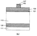
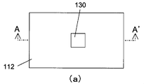
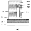
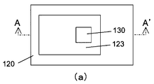
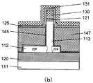
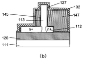
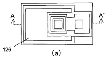
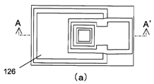
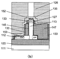
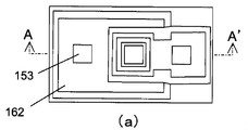
- FIG. 37 (a) is a plan view of an NMOS SGT formed using the present invention
- FIG. 37 (b) is a cross-sectional view taken along the cut line AA ′ of FIG. 37 (a).
- An NMOS SGT formed using the present invention will be described below with reference to FIG.
- a planar silicon layer 112 is formed on the BOX layer 120 formed on the Si substrate 111
- a columnar silicon layer 113 is formed on the planar silicon layer 112, and a high dielectric film is formed around the columnar silicon layer 113.
- a gate insulating film 145 and a metal gate electrode 147 are formed.
- N + source diffusion layer 200 is formed on the planar silicon layer 112 below the columnar silicon layer, and an N + drain diffusion layer 201 is formed on the columnar silicon layer.
- a contact 174 is formed on the N + source diffusion layer 200, a contact 173 is formed on the N + drain diffusion layer 201, and a contact 172 is formed on the gate wiring 147b extending from the gate electrode 147a.
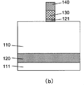
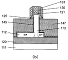
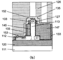
- FIG. 38 is a cross-sectional view taken along the cut line BB ′ of FIG.
- Wa is the length from the center of the silicon pillar 113 to the end of the planar silicon layer 112
- Wp is the length from the center of the silicon pillar 113 to the side wall
- Wox is the thickness of the gate insulating film 145
- Wg is the gate electrode 147.
- Ws is the width of the oxide film sidewall and the nitride film sidewall, that is, the width of the insulating film.
- the SGT operates as a transistor by connecting the N + source diffusion layer to the GND potential, connecting the N + drain diffusion layer to the Vcc potential, and applying a potential of 0 to Vcc to the gate electrode.
- the N + diffusion layer formed on the columnar silicon layer may be an N + source diffusion layer
- the N + diffusion layer formed on the planar silicon layer below the columnar silicon layer may be an N + drain diffusion layer.
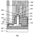
- FIG. 1 shows a manufacturing process for forming the SGT of the present invention
- FIGS. 2 to 37 show an example of manufacturing the SGT according to the present invention.
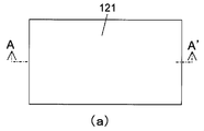
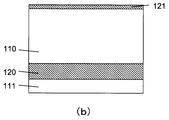
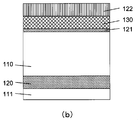
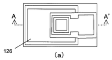
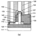
- (A) is a plan view
- (b) is a cross-sectional view along A-A ′.
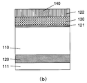
- pad oxide film 121 is formed on SOI layer 110 using an SOI substrate in which BOX layer 120 is formed on Si substrate 111 and silicon layer 110 is formed on BOX layer 120. .
- lot formation may be performed, laser mark formation may be performed, and pad oxide film cleaning may be performed. Further, the pad oxide film thickness may be measured after the pad oxidation (steps 1, 2, 3, 4, 5 in FIG. 1).
- Impurity implantation for threshold adjustment may be performed on the SOI layer through the pad oxide film, annealing may be performed for impurity activation and diffusion, and the impurity distribution in the SOI layer may be made uniform. At this time, the number of manufacturing steps can be reduced by using a pad oxide film formed as a through oxide film at the time of impurity implantation in order to relieve stress between the silicon nitride film and silicon formed in the next process. And manufacturing costs can be reduced.
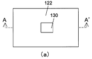
- a silicon nitride film 130 as a first hard mask is formed, and then a silicon oxide film 122 is formed.
- the nitride film thickness may be measured.
- the oxide film thickness may be measured after the silicon oxide film is deposited (steps 6, 7, 8, and 9 in FIG. 1).
- a resist is applied, a pattern is formed by inverting the columnar silicon layer with lithography using lithography, and a hole penetrating the silicon oxide film 122 is formed at a position where the columnar silicon layer is formed by dry etching. .
- Dimensional measurement and inspection may be performed after lithography. Further, cleaning may be performed after etching (steps 10, 11, 12, 13, 14, 15, 16, and 17 in FIG. 1).
- an oxide film 129 is deposited, and referring to FIG. 41, the oxide film 129 is etched back to reduce the diameter of the hole penetrating the silicon oxide film 122. it can.
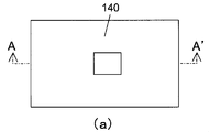
- amorphous silicon or polysilicon 140 is formed so as to fill holes formed in silicon oxide film 122. Cleaning may be performed before depositing amorphous silicon or polysilicon. In addition, the film thickness may be measured after deposition (steps 18, 19, and 20 in FIG. 1).
- amorphous silicon or polysilicon 140 on silicon oxide film 122 is polished and removed by CMP (chemical mechanical polishing). After polishing, the film thickness may be measured (steps 21 and 22 in FIG. 1).
- the silicon oxide film 122 is removed by wet etching using hydrofluoric acid or the like, or by dry etching, so that amorphous silicon or poly silicon serving as a second hard mask at the time of dry etching of the columnar silicon layer in a later process is obtained. Silicon 140 is formed. (Step 23 in FIG. 1)
- amorphous silicon or polysilicon 140 is sacrificial oxidized to form silicon oxide film 128, and the dimensions of amorphous silicon or polysilicon are reduced.
- cleaning before sacrificial oxidation may be performed.
- the film thickness may be measured after oxidation (steps 24, 25, and 26 in FIG. 1).
- the silicon oxide film 128 on the surface of amorphous silicon or polysilicon 140 is removed by wet etching using hydrofluoric acid or dry etching. (Step 27 in FIG. 1).
- silicon nitride film 130 and pad oxide film 121 as the first hard mask are etched by dry etching using amorphous silicon or polysilicon 140 as the second hard mask as a mask. (Steps 28 and 29 in FIG. 1).
- columnar silicon layer 113 is formed by dry etching using silicon nitride film 130 as the first hard mask and amorphous silicon or polysilicon 140 as the second hard mask as a mask. After etching, organic matter removal, inspection using SEM, and step confirmation may be performed (steps 30, 31, 32, and 33 in FIG. 1). During dry etching, the amorphous silicon or polysilicon 140, which is the second hard mask, is also etched. When all of the amorphous silicon or polysilicon 140 is etched, the plasma emission intensity that can be detected by the dry etching apparatus changes. Therefore, by detecting the change in the plasma emission intensity, the end point of etching can be detected, and the height of the columnar silicon layer 113 can be stably controlled regardless of the etching rate.
- the film thickness of amorphous silicon or polysilicon 140 before the columnar silicon layer dry etching needs to be smaller than the height of the columnar silicon layer.
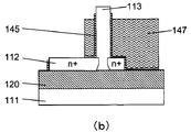
- the planar silicon layer 112 is formed on the buried oxide film layer 120.
- the surface of the columnar silicon layer and the planar silicon layer are used to alleviate the unevenness of the side wall of the columnar silicon layer 113 serving as a channel portion and to remove the silicon surface into which carbon or the like is implanted during dry etching.
- Sacrificial oxidation is performed to form a sacrificial oxide film 123.
- cleaning before sacrificial oxidation may be performed.
- the sacrificial oxide film thickness may be measured after the sacrificial oxidation (steps 34, 35, and 36 in FIG. 1).
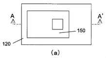
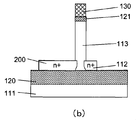
- a resist 150 is applied, and a pattern of the source diffusion layer is formed from the resist using lithography.
- overlay error measurement, dimension measurement, and inspection may be performed (steps 37, 38, 39, 40, and 41 in FIG. 1).
- the sacrificial oxide film 123 formed by the above-described sacrificial oxidation on the columnar silicon layer 113 and the planar silicon layer 112 protects the silicon surface from contamination such as by-products generated during the next dry etching.
- planar silicon layer 112 is processed by dry etching, and planar silicon layer 112 is separated. (FIG. 1, steps 42 and 43)
- step confirmation may be performed (steps 44, 45, and 46 in FIG. 1).
- impurities such as P and As are introduced into the surface of planar silicon layer 112 by impurity implantation or the like to form N + source diffusion layer 200 (steps 47 and 48 in FIG. 1).
- the number of manufacturing steps can be reduced by using the sacrificial oxide film 123 formed during the sacrificial oxidation of the columnar silicon layer 113 and the planar silicon layer 112 as a through oxide film.
- the transistor characteristics may fluctuate. Therefore, it is essential that the widths Wp1 and pWp2 of the columnar silicon pillars are smaller than Wn which is the width of the nitride film 130.
- Wp1 is the width of the lower part of the columnar silicon layer
- Wp2 is the width of the upper part of the columnar silicon layer.
- the impurities are not implanted from the side wall of the columnar silicon layer 113 at the time of implantation, it is preferable to implant the impurities at a small angle, that is, 0 to 6 degrees.
- the silicon nitride film 130 formed on the columnar silicon layer 113 is not implanted into the upper portion of the columnar silicon layer 113.
- the implantation into the N + source diffusion layer 200 is preferably 0 °, but the implantation into the drain diffusion layer, which will be formed later on the columnar silicon layer 113, is formed in a self-aligned manner with the gate electrode. It is preferable to inject it.
- the silicon surface is oxidized to form oxide film 124, and nitride film 130 is thinned by wet etching. Cleaning may be performed before oxidation. In addition, the film thickness may be measured after oxidation. (Steps 49, 50, 51, 52 in FIG. 1). This step is for removing the high-K gate insulating film using dry etching in FIG. 22, and the width Wn of the nitride film 130 needs to be smaller than the widths Wp1 and Wp2 of the silicon pillar 113.
- sacrificial oxide film 123 and oxide film 124 are removed by wet etching using hydrofluoric acid or the like. (Step 53 in FIG. 1)
- HfSiO and HfSiON are formed as high-K gate insulating film 145. Cleaning may be performed before forming the insulating film. Further, heat treatment may be performed after the formation (steps 54, 55, and 56 in FIG. 1).
- metal 147 is formed as a gate conductive film so as to embed columnar silicon layer 113. (Step 57 in FIG. 1)
- metal 147 is polished by CMP to planarize the upper surface of the gate conductive film.
- CMP by using the silicon nitride film 130, which is the first hard mask, as a CMP stopper, the CMP polishing amount can be controlled with good reproducibility. (Step 58 in FIG. 1)
- the gate length is determined by etching back metal 147 which is a gate conductive film.
- the high-K gate insulating film is also etched (step 59 in FIG. 1).
- the film thickness may be measured after metal deposition (step 60 in FIG. 1).
- a silicon oxide film 125 is formed on the surfaces of metal 147 and silicon pillar 113 which are gate conductive films. By covering the metal 147 with the silicon oxide film 125, it can be processed without considering metal contamination in a later process. In addition, since the gate upper surface is protected from wet processing or dry processing, variation in gate length, that is, variation in gate length and damage to the gate insulating film 145 from the gate upper surface can be suppressed. (FIG. 1, step 61)
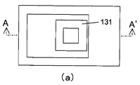
- a silicon nitride film 131 thicker than the desired gate electrode is formed. After film formation, the nitride film thickness may be measured (steps 62 and 63 in FIG. 1).
- silicon nitride film 131 is etched back to form silicon nitride film 131 sidewalls.
- the silicon oxide film 125 is also etched.
- organic substance removal and shape measurement may be performed (steps 64, 65, 66 in FIG. 1). Since the sum of the thickness of the silicon nitride film sidewall 131 and the thickness of the silicon oxide film is the sum of the thickness of the gate electrode formed of the gate electrode 147 made of the metal 147 and the thickness of the high-K gate insulating film.
- a gate electrode having a desired film thickness can be formed.
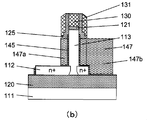
- BARC layer 161 and resist 160 are applied, and a gate wiring pattern is formed by resist 160 using lithography. After pattern formation, overlay error measurement, dimension measurement, and inspection may be performed (steps 67, 68, 69, 70, 71 in FIG. 1).
- BARC layer 161 gate conductive film metal 147, and high-K gate insulating film are etched to form gate electrode 147a and gate wiring pattern 147b. And the BARC layer is removed. Thereafter, shape measurement may be performed (steps 72, 73, 74, 75, and 76 in FIG. 1).
- silicon nitride film 130 and silicon nitride film sidewall 131 and silicon oxide films 121 and 125 on columnar silicon 113, and oxide film 124 on a planar silicon layer are removed by dry etching or wet etching (see FIG. 28).
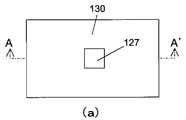
- a silicon oxide film 127 and a silicon nitride film 132 are formed. After film formation, the film thickness may be measured (steps 78, 79, and 80 in FIG. 1).
- silicon nitride film 132 is etched back, silicon oxide film 127 is etched to expose the upper surface of N + source diffusion layer 200 and the upper surface of columnar silicon 113, and the sidewall and gate of columnar silicon layer 113. 147 side walls are covered with silicon nitride films 133 and 134. After etching, organic matter removal and shape measurement may be performed (steps 81, 82, and 83 in FIG. 1). Since the nitride films 133 and 134 separate the gate electrode 147, the source diffusion layer 200, and the N + drain diffusion layer formed later on the columnar silicon, the gate electrodes 147, 147, the source diffusion layer 200, and the drain diffusion layer made of silicide are separated. Can be prevented.
- the silicon nitride films 133 and 134 are silicon oxide films, they are etched by hydrofluoric acid used for cleaning / peeling process and silicide pretreatment, so that the silicon nitride films 133 and 134 are films not soluble in hydrofluoric acid such as silicon nitride films. Preferably there is.
- an impurity such as P or As is introduced into the upper portion of columnar silicon layer 113 by impurity implantation or the like, and N + drain diffusion layer 201 is formed. Activation may be performed after the introduction of impurities (steps 84 and 85 in FIG. 1).
- a metal film such as Ni or Co is sputtered, and heat treatment is applied to make the surface of source 200 drain 201 a silicide of a metal and a semiconductor, that is, silicidation, thereby removing the unreacted metal film.
- a silicide layer 152 on the diffusion layer 201 and a silicide layer 153 on the source diffusion layer 200 are formed.
- the oxide film may be removed (steps 86, 87, 88, 89 in FIG. 1).
- a silicon nitride film or the like is formed as contact stopper 135. (Step 90 in FIG. 1)
- a silicon oxide film is formed as interlayer film 126, it is planarized by CMP. After film formation, the film thickness may be measured. Further, the film thickness may be measured after planarization. Further, the nitride film thickness may be measured (steps 91, 92, 93, 94, 95 in FIG. 1).
- contact holes are formed by etching on drain diffusion layer 201 above columnar silicon layer 113, on gate wiring 147b, and on source diffusion layer 200. Before etching the contact hole, contact mask exposure is performed. Further, dimension measurement, overlay error measurement, and inspection may be performed. Further, after the contact hole is formed, the plasma resist is peeled off. Thereafter, cleaning may be performed, and dimension measurement, oxide film thickness measurement, inspection, and wafer container replacement may be performed (FIG. 1 steps 96, 97, 98, 99, 100, 101, 102, 103, 104, 105, 106, 107, 108).
- the etching depth of the contact hole on the columnar silicon layer and the contact hole on the gate wiring is different from the etching depth of the contact hole on the planar silicon layer below the columnar silicon layer.
- the interlayer film between the contact hole on the silicon layer and the contact hole on the gate wiring is etched.
- the interlayer between the contact holes on the planar silicon layer below the columnar silicon layer is masked using the resist 162 as a mask.
- the contact stopper may be etched after the film is etched and the interlayer film is etched.
- the interlayer film of the contact hole on the upper part of the columnar silicon layer is etched, and the contact hole on the gate wiring and the contact on the planar silicon layer below the columnar silicon layer are referred to with reference to FIG.
- the contact stopper may be etched after the interlayer film of the hole is etched and the interlayer film is etched.
- the upper part of the pillar-shaped silicon layer is etched by separately etching the interlayer film in the contact hole above the pillar-shaped silicon layer and the interlayer film in the contact hole on the planar silicon layer below the pillar-shaped silicon layer and the contact hole on the gate wiring. It is also possible to optimize the etching conditions for the contact holes and the etching conditions for the contact holes on the gate wiring and the contact holes on the planar silicon layer below the columnar silicon layer.
- tantalum (Ta), tantalum nitride (TaN) or the like, which is barrier metal 171 is formed in the contact hole, and then copper (Cu) 170 is formed by sputtering or plating, and contact 172 is formed by CMP. , 173, 174.
- Titanium (Ti) or titanium nitride (TiN) may be used as the barrier metal.
- tungsten (W) may be used.
- an alloy containing copper may be used.
- backside treatment, inspection, and heat treatment may be performed. Further, inspection may be performed after CMP (steps 111, 112, 113, 114, and 115 in FIG. 1).
- SiC 180 (silicon carbide) is formed as an etching stopper for the first layer wiring, and subsequently, a Low-k film 190 which is an interlayer film of the first wiring layer is formed.
- the film thickness may be measured and inspected (steps 116, 117, 118, and 119 in FIG. 1).
- the first layer wiring is patterned to form a groove pattern of the first wiring layer. After patterning, dimension measurement, overlay error measurement, and inspection may be performed. After forming the groove pattern, the plasma resist may be stripped and inspected (steps 120, 121, 122, 123, 124, 125, 126, 127 in FIG. 1).
- first layer wirings 177, 178, 179 are formed by CMP.
- Titanium (Ti) or titanium nitride (TiN) may be used as the barrier metal.
- tungsten (W) may be used.
- an alloy containing copper may be used.
- backside treatment, inspection, and heat treatment may be performed. In addition, inspection may be performed after CMP (steps 128, 129, 130, 131, 132, 133, and 134 in FIG. 1).
- nitride film deposition, interlayer insulating film deposition, and interlayer insulating film thickness measurement may be performed (steps 135, 136, and 137 in FIG. 1).
- Multi-layer wiring may be performed before the pad via.
- the manufacturing method of the semiconductor device of this invention The top view which shows the manufacture example of the semiconductor device which concerns on this invention.
- A-A 'sectional process drawing showing a manufacturing example of a semiconductor device according to the present invention The top view which shows the manufacture example of the semiconductor device which concerns on this invention.
- A-A 'sectional process drawing showing a manufacturing example of a semiconductor device according to the present invention The top view which shows the manufacture example of the semiconductor device which concerns on this invention.
- A-A 'sectional process drawing showing a manufacturing example of a semiconductor device according to the present invention The top view which shows the manufacture example of the semiconductor device which concerns on this invention.
- A-A 'sectional process drawing showing a manufacturing example of a semiconductor device according to the present invention The top view which shows the manufacture example of the semiconductor device which concerns on this invention.
- A-A 'sectional process drawing showing a manufacturing example of a semiconductor device according to the present invention The top view which shows the manufacture example of the semiconductor device which concerns on this invention.
- A-A 'sectional process drawing showing a manufacturing example of a semiconductor device according to the present invention The top view which shows the manufacture example of the semiconductor device which concerns on this invention.
- A-A 'sectional process drawing showing a manufacturing example of a semiconductor device according to the present invention The top view which shows the manufacture example of the semiconductor device which concerns on this invention.
- FIG. 38 is a cross-sectional view of FIG.
- A-A 'sectional process drawing showing a manufacturing example of a semiconductor device according to the present invention The top view which shows the manufacture example of the semiconductor device which concerns on this invention.
- A-A 'sectional process drawing showing a manufacturing example of a semiconductor device according to the present invention The top view which shows the manufacture example of the semiconductor device which concerns on this invention.
- Silicide layer 153 Silicide layer 160. Resist 161. BARC layer 162. Resist 170. Cu 171. Barrier metal 172. Contact 173. Contact 174. Contact 175. Barrier metal 176. Cu 177. First layer wiring 178. First layer wiring 179. First layer wiring 200. N + source diffusion layer 201. N + drain diffusion layer
Landscapes
- Insulated Gate Type Field-Effect Transistor (AREA)
- Electrodes Of Semiconductors (AREA)
- Semiconductor Memories (AREA)
Abstract
Priority Applications (5)
| Application Number | Priority Date | Filing Date | Title |
|---|---|---|---|
| EP09709836.2A EP2244303A4 (fr) | 2008-02-15 | 2009-02-16 | Dispositif semiconducteur et procédé pour sa fabrication |
| CN200980105298XA CN101946329B (zh) | 2008-02-15 | 2009-02-16 | 半导体器件及其制造方法 |
| JP2009553484A JP5340180B2 (ja) | 2008-02-15 | 2009-02-16 | 半導体装置とその製造方法 |
| KR1020107020178A KR101124040B1 (ko) | 2008-02-15 | 2009-02-16 | 반도체 장치와 그 제조방법 |
| US12/704,000 US8241976B2 (en) | 2008-02-15 | 2010-02-11 | Semiconductor surrounding gate transistor device and production method therefor |
Applications Claiming Priority (2)
| Application Number | Priority Date | Filing Date | Title |
|---|---|---|---|
| JPPCT/JP2008/052566 | 2008-02-15 | ||
| PCT/JP2008/052566 WO2009110049A1 (fr) | 2008-02-15 | 2008-02-15 | Dispositif semiconducteur et procédé pour sa fabrication |
Related Child Applications (1)
| Application Number | Title | Priority Date | Filing Date |
|---|---|---|---|
| US12/704,000 Continuation US8241976B2 (en) | 2008-02-15 | 2010-02-11 | Semiconductor surrounding gate transistor device and production method therefor |
Publications (1)
| Publication Number | Publication Date |
|---|---|
| WO2009102060A1 true WO2009102060A1 (fr) | 2009-08-20 |
Family
ID=40957089
Family Applications (2)
| Application Number | Title | Priority Date | Filing Date |
|---|---|---|---|
| PCT/JP2008/052566 Ceased WO2009110049A1 (fr) | 2008-02-15 | 2008-02-15 | Dispositif semiconducteur et procédé pour sa fabrication |
| PCT/JP2009/052558 Ceased WO2009102060A1 (fr) | 2008-02-15 | 2009-02-16 | Dispositif semiconducteur et procédé pour sa fabrication |
Family Applications Before (1)
| Application Number | Title | Priority Date | Filing Date |
|---|---|---|---|
| PCT/JP2008/052566 Ceased WO2009110049A1 (fr) | 2008-02-15 | 2008-02-15 | Dispositif semiconducteur et procédé pour sa fabrication |
Country Status (5)
| Country | Link |
|---|---|
| EP (1) | EP2244303A4 (fr) |
| KR (1) | KR101124040B1 (fr) |
| CN (1) | CN101946329B (fr) |
| TW (1) | TW200939359A (fr) |
| WO (2) | WO2009110049A1 (fr) |
Cited By (1)
| Publication number | Priority date | Publication date | Assignee | Title |
|---|---|---|---|---|
| JP2016225641A (ja) * | 2016-08-05 | 2016-12-28 | ユニサンティス エレクトロニクス シンガポール プライベート リミテッドUnisantis Electronics Singapore Pte Ltd. | 半導体装置 |
Families Citing this family (3)
| Publication number | Priority date | Publication date | Assignee | Title |
|---|---|---|---|---|
| CN109637927B (zh) * | 2018-12-12 | 2020-11-24 | 上海华力集成电路制造有限公司 | 金属栅的制造方法 |
| TWI762943B (zh) * | 2020-06-04 | 2022-05-01 | 新唐科技股份有限公司 | 半導體結構以及半導體結構的製造方法 |
| KR102780784B1 (ko) * | 2020-10-20 | 2025-03-13 | 삼성전자주식회사 | 반도체 장치 제조 방법 |
Citations (6)
| Publication number | Priority date | Publication date | Assignee | Title |
|---|---|---|---|---|
| JPS6113661A (ja) * | 1984-06-29 | 1986-01-21 | Nippon Telegr & Teleph Corp <Ntt> | 半導体装置およびその製造方法 |
| JPH0271556A (ja) | 1988-09-06 | 1990-03-12 | Toshiba Corp | 半導体装置 |
| JPH02188966A (ja) | 1989-01-17 | 1990-07-25 | Toshiba Corp | Mos型半導体装置 |
| JPH03145761A (ja) | 1989-11-01 | 1991-06-20 | Toshiba Corp | 半導体装置 |
| JP2000068516A (ja) * | 1998-08-24 | 2000-03-03 | Sony Corp | 半導体装置とその製造方法 |
| JP2003179160A (ja) * | 2001-10-18 | 2003-06-27 | Chartered Semiconductor Mfg Ltd | 縦形デバイスの集積化を用いて自己整合性cmosインバータを形成する方法 |
Family Cites Families (4)
| Publication number | Priority date | Publication date | Assignee | Title |
|---|---|---|---|---|
| DE19746901C2 (de) * | 1997-10-23 | 1999-08-12 | Siemens Ag | Verfahren zur Herstellung eines vertikalen MOS-Transistors |
| DE19746900C2 (de) * | 1997-10-23 | 2002-02-14 | Infineon Technologies Ag | Vertikaler MOS-Transistor und Verfahren zu dessen Herstellung |
| US6229161B1 (en) * | 1998-06-05 | 2001-05-08 | Stanford University | Semiconductor capacitively-coupled NDR device and its applications in high-density high-speed memories and in power switches |
| KR100537103B1 (ko) * | 2003-12-27 | 2005-12-16 | 동부아남반도체 주식회사 | 수직형 트랜지스터의 제조방법 |
-
2008
- 2008-02-15 WO PCT/JP2008/052566 patent/WO2009110049A1/fr not_active Ceased
-
2009
- 2009-02-12 TW TW098104442A patent/TW200939359A/zh unknown
- 2009-02-16 EP EP09709836.2A patent/EP2244303A4/fr not_active Withdrawn
- 2009-02-16 CN CN200980105298XA patent/CN101946329B/zh active Active
- 2009-02-16 KR KR1020107020178A patent/KR101124040B1/ko active Active
- 2009-02-16 WO PCT/JP2009/052558 patent/WO2009102060A1/fr not_active Ceased
Patent Citations (6)
| Publication number | Priority date | Publication date | Assignee | Title |
|---|---|---|---|---|
| JPS6113661A (ja) * | 1984-06-29 | 1986-01-21 | Nippon Telegr & Teleph Corp <Ntt> | 半導体装置およびその製造方法 |
| JPH0271556A (ja) | 1988-09-06 | 1990-03-12 | Toshiba Corp | 半導体装置 |
| JPH02188966A (ja) | 1989-01-17 | 1990-07-25 | Toshiba Corp | Mos型半導体装置 |
| JPH03145761A (ja) | 1989-11-01 | 1991-06-20 | Toshiba Corp | 半導体装置 |
| JP2000068516A (ja) * | 1998-08-24 | 2000-03-03 | Sony Corp | 半導体装置とその製造方法 |
| JP2003179160A (ja) * | 2001-10-18 | 2003-06-27 | Chartered Semiconductor Mfg Ltd | 縦形デバイスの集積化を用いて自己整合性cmosインバータを形成する方法 |
Non-Patent Citations (1)
| Title |
|---|
| See also references of EP2244303A4 |
Cited By (1)
| Publication number | Priority date | Publication date | Assignee | Title |
|---|---|---|---|---|
| JP2016225641A (ja) * | 2016-08-05 | 2016-12-28 | ユニサンティス エレクトロニクス シンガポール プライベート リミテッドUnisantis Electronics Singapore Pte Ltd. | 半導体装置 |
Also Published As
| Publication number | Publication date |
|---|---|
| TW200939359A (en) | 2009-09-16 |
| KR101124040B1 (ko) | 2012-03-23 |
| CN101946329A (zh) | 2011-01-12 |
| WO2009110049A1 (fr) | 2009-09-11 |
| CN101946329B (zh) | 2012-06-27 |
| KR20100120205A (ko) | 2010-11-12 |
| EP2244303A4 (fr) | 2013-10-09 |
| EP2244303A1 (fr) | 2010-10-27 |
Similar Documents
| Publication | Publication Date | Title |
|---|---|---|
| JP6002310B2 (ja) | 半導体装置の製造方法 | |
| JP5622335B2 (ja) | 半導体装置の製造方法 | |
| JP4577592B2 (ja) | 半導体装置の製造方法 | |
| KR101124137B1 (ko) | 반도체 장치 및 그 제조방법 | |
| JP6014726B2 (ja) | 半導体装置及びその製造方法 | |
| WO2009102060A1 (fr) | Dispositif semiconducteur et procédé pour sa fabrication | |
| JP5632055B2 (ja) | 半導体装置及びその製造方法 | |
| JP5779702B2 (ja) | 半導体装置及びその製造方法 | |
| JP5356260B2 (ja) | 半導体装置及びその製造方法 | |
| JP5340180B2 (ja) | 半導体装置とその製造方法 | |
| JP5356258B2 (ja) | 半導体装置の製造方法 |
Legal Events
| Date | Code | Title | Description |
|---|---|---|---|
| WWE | Wipo information: entry into national phase |
Ref document number: 200980105298.X Country of ref document: CN |
|
| 121 | Ep: the epo has been informed by wipo that ep was designated in this application |
Ref document number: 09709836 Country of ref document: EP Kind code of ref document: A1 |
|
| WWE | Wipo information: entry into national phase |
Ref document number: 2009553484 Country of ref document: JP |
|
| WWE | Wipo information: entry into national phase |
Ref document number: 5464/DELNP/2010 Country of ref document: IN |
|
| NENP | Non-entry into the national phase |
Ref country code: DE |
|
| WWE | Wipo information: entry into national phase |
Ref document number: 2009709836 Country of ref document: EP |
|
| ENP | Entry into the national phase |
Ref document number: 20107020178 Country of ref document: KR Kind code of ref document: A |