WO2009104536A1 - 半導体チップ及び半導体装置 - Google Patents
半導体チップ及び半導体装置 Download PDFInfo
- Publication number
- WO2009104536A1 WO2009104536A1 PCT/JP2009/052493 JP2009052493W WO2009104536A1 WO 2009104536 A1 WO2009104536 A1 WO 2009104536A1 JP 2009052493 W JP2009052493 W JP 2009052493W WO 2009104536 A1 WO2009104536 A1 WO 2009104536A1
- Authority
- WO
- WIPO (PCT)
- Prior art keywords
- chip
- semiconductor
- region
- semiconductor chip
- memory
- Prior art date
- Legal status (The legal status is an assumption and is not a legal conclusion. Google has not performed a legal analysis and makes no representation as to the accuracy of the status listed.)
- Ceased
Links
Images


Classifications
-
- H—ELECTRICITY
- H10—SEMICONDUCTOR DEVICES; ELECTRIC SOLID-STATE DEVICES NOT OTHERWISE PROVIDED FOR
- H10W—GENERIC PACKAGES, INTERCONNECTIONS, CONNECTORS OR OTHER CONSTRUCTIONAL DETAILS OF DEVICES COVERED BY CLASS H10
- H10W72/00—Interconnections or connectors in packages
-
- H—ELECTRICITY
- H10—SEMICONDUCTOR DEVICES; ELECTRIC SOLID-STATE DEVICES NOT OTHERWISE PROVIDED FOR
- H10W—GENERIC PACKAGES, INTERCONNECTIONS, CONNECTORS OR OTHER CONSTRUCTIONAL DETAILS OF DEVICES COVERED BY CLASS H10
- H10W72/00—Interconnections or connectors in packages
- H10W72/30—Die-attach connectors
-
- H—ELECTRICITY
- H10—SEMICONDUCTOR DEVICES; ELECTRIC SOLID-STATE DEVICES NOT OTHERWISE PROVIDED FOR
- H10W—GENERIC PACKAGES, INTERCONNECTIONS, CONNECTORS OR OTHER CONSTRUCTIONAL DETAILS OF DEVICES COVERED BY CLASS H10
- H10W72/00—Interconnections or connectors in packages
- H10W72/50—Bond wires
-
- H—ELECTRICITY
- H10—SEMICONDUCTOR DEVICES; ELECTRIC SOLID-STATE DEVICES NOT OTHERWISE PROVIDED FOR
- H10W—GENERIC PACKAGES, INTERCONNECTIONS, CONNECTORS OR OTHER CONSTRUCTIONAL DETAILS OF DEVICES COVERED BY CLASS H10
- H10W72/00—Interconnections or connectors in packages
- H10W72/01—Manufacture or treatment
- H10W72/013—Manufacture or treatment of die-attach connectors
- H10W72/01308—Manufacture or treatment of die-attach connectors using permanent auxiliary members, e.g. using alignment marks
-
- H—ELECTRICITY
- H10—SEMICONDUCTOR DEVICES; ELECTRIC SOLID-STATE DEVICES NOT OTHERWISE PROVIDED FOR
- H10W—GENERIC PACKAGES, INTERCONNECTIONS, CONNECTORS OR OTHER CONSTRUCTIONAL DETAILS OF DEVICES COVERED BY CLASS H10
- H10W72/00—Interconnections or connectors in packages
- H10W72/071—Connecting or disconnecting
- H10W72/072—Connecting or disconnecting of bump connectors
- H10W72/07251—Connecting or disconnecting of bump connectors characterised by changes in properties of the bump connectors during connecting
-
- H—ELECTRICITY
- H10—SEMICONDUCTOR DEVICES; ELECTRIC SOLID-STATE DEVICES NOT OTHERWISE PROVIDED FOR
- H10W—GENERIC PACKAGES, INTERCONNECTIONS, CONNECTORS OR OTHER CONSTRUCTIONAL DETAILS OF DEVICES COVERED BY CLASS H10
- H10W72/00—Interconnections or connectors in packages
- H10W72/071—Connecting or disconnecting
- H10W72/073—Connecting or disconnecting of die-attach connectors
- H10W72/07311—Treating the bonding area before connecting, e.g. by applying flux or cleaning
-
- H—ELECTRICITY
- H10—SEMICONDUCTOR DEVICES; ELECTRIC SOLID-STATE DEVICES NOT OTHERWISE PROVIDED FOR
- H10W—GENERIC PACKAGES, INTERCONNECTIONS, CONNECTORS OR OTHER CONSTRUCTIONAL DETAILS OF DEVICES COVERED BY CLASS H10
- H10W72/00—Interconnections or connectors in packages
- H10W72/20—Bump connectors, e.g. solder bumps or copper pillars; Dummy bumps; Thermal bumps
- H10W72/241—Dispositions, e.g. layouts
- H10W72/247—Dispositions of multiple bumps
- H10W72/248—Top-view layouts, e.g. mirror arrays
-
- H—ELECTRICITY
- H10—SEMICONDUCTOR DEVICES; ELECTRIC SOLID-STATE DEVICES NOT OTHERWISE PROVIDED FOR
- H10W—GENERIC PACKAGES, INTERCONNECTIONS, CONNECTORS OR OTHER CONSTRUCTIONAL DETAILS OF DEVICES COVERED BY CLASS H10
- H10W72/00—Interconnections or connectors in packages
- H10W72/20—Bump connectors, e.g. solder bumps or copper pillars; Dummy bumps; Thermal bumps
- H10W72/251—Materials
-
- H—ELECTRICITY
- H10—SEMICONDUCTOR DEVICES; ELECTRIC SOLID-STATE DEVICES NOT OTHERWISE PROVIDED FOR
- H10W—GENERIC PACKAGES, INTERCONNECTIONS, CONNECTORS OR OTHER CONSTRUCTIONAL DETAILS OF DEVICES COVERED BY CLASS H10
- H10W72/00—Interconnections or connectors in packages
- H10W72/30—Die-attach connectors
- H10W72/381—Auxiliary members
- H10W72/387—Flow barriers
-
- H—ELECTRICITY
- H10—SEMICONDUCTOR DEVICES; ELECTRIC SOLID-STATE DEVICES NOT OTHERWISE PROVIDED FOR
- H10W—GENERIC PACKAGES, INTERCONNECTIONS, CONNECTORS OR OTHER CONSTRUCTIONAL DETAILS OF DEVICES COVERED BY CLASS H10
- H10W72/00—Interconnections or connectors in packages
- H10W72/50—Bond wires
- H10W72/551—Materials of bond wires
- H10W72/552—Materials of bond wires comprising metals or metalloids, e.g. silver
- H10W72/5524—Materials of bond wires comprising metals or metalloids, e.g. silver comprising aluminium [Al]
-
- H—ELECTRICITY
- H10—SEMICONDUCTOR DEVICES; ELECTRIC SOLID-STATE DEVICES NOT OTHERWISE PROVIDED FOR
- H10W—GENERIC PACKAGES, INTERCONNECTIONS, CONNECTORS OR OTHER CONSTRUCTIONAL DETAILS OF DEVICES COVERED BY CLASS H10
- H10W72/00—Interconnections or connectors in packages
- H10W72/50—Bond wires
- H10W72/551—Materials of bond wires
- H10W72/552—Materials of bond wires comprising metals or metalloids, e.g. silver
- H10W72/5525—Materials of bond wires comprising metals or metalloids, e.g. silver comprising copper [Cu]
-
- H—ELECTRICITY
- H10—SEMICONDUCTOR DEVICES; ELECTRIC SOLID-STATE DEVICES NOT OTHERWISE PROVIDED FOR
- H10W—GENERIC PACKAGES, INTERCONNECTIONS, CONNECTORS OR OTHER CONSTRUCTIONAL DETAILS OF DEVICES COVERED BY CLASS H10
- H10W74/00—Encapsulations, e.g. protective coatings
- H10W74/10—Encapsulations, e.g. protective coatings characterised by their shape or disposition
- H10W74/15—Encapsulations, e.g. protective coatings characterised by their shape or disposition on active surfaces of flip-chip devices, e.g. underfills
-
- H—ELECTRICITY
- H10—SEMICONDUCTOR DEVICES; ELECTRIC SOLID-STATE DEVICES NOT OTHERWISE PROVIDED FOR
- H10W—GENERIC PACKAGES, INTERCONNECTIONS, CONNECTORS OR OTHER CONSTRUCTIONAL DETAILS OF DEVICES COVERED BY CLASS H10
- H10W90/00—Package configurations
-
- H—ELECTRICITY
- H10—SEMICONDUCTOR DEVICES; ELECTRIC SOLID-STATE DEVICES NOT OTHERWISE PROVIDED FOR
- H10W—GENERIC PACKAGES, INTERCONNECTIONS, CONNECTORS OR OTHER CONSTRUCTIONAL DETAILS OF DEVICES COVERED BY CLASS H10
- H10W90/00—Package configurations
- H10W90/701—Package configurations characterised by the relative positions of pads or connectors relative to package parts
- H10W90/721—Package configurations characterised by the relative positions of pads or connectors relative to package parts of bump connectors
- H10W90/724—Package configurations characterised by the relative positions of pads or connectors relative to package parts of bump connectors between a chip and a stacked insulating package substrate, interposer or RDL
-
- H—ELECTRICITY
- H10—SEMICONDUCTOR DEVICES; ELECTRIC SOLID-STATE DEVICES NOT OTHERWISE PROVIDED FOR
- H10W—GENERIC PACKAGES, INTERCONNECTIONS, CONNECTORS OR OTHER CONSTRUCTIONAL DETAILS OF DEVICES COVERED BY CLASS H10
- H10W90/00—Package configurations
- H10W90/701—Package configurations characterised by the relative positions of pads or connectors relative to package parts
- H10W90/731—Package configurations characterised by the relative positions of pads or connectors relative to package parts of die-attach connectors
- H10W90/734—Package configurations characterised by the relative positions of pads or connectors relative to package parts of die-attach connectors between a chip and a stacked insulating package substrate, interposer or RDL
Definitions
- the present invention relates to a semiconductor chip (for example, a memory chip, a logic circuit chip, etc.) and a semiconductor device including the same.
- a semiconductor chip for example, a memory chip, a logic circuit chip, etc.
- a semiconductor device including the same.
- SIP system in package
- solder bumps made of solder, gold or copper are generated after applying additional wiring on the semiconductor circuit main surface of the semiconductor chip as necessary.
- Patent Documents 1 to 7 proposals have been made in the past for devising the position and shape of electrodes and mounting structures for various purposes with respect to semiconductor chips.
- the formation region of the semiconductor circuit (memory circuit or logic circuit) formed on the semiconductor chip is divided.
- an electrode is also provided by being distributed (aggregated) in the vicinity of the central portion of the gap region formed between the divided semiconductor circuit forming regions. This is performed in order to minimize the signal input / output wiring formation efficiency for the divided semiconductor circuits and the chip occupation area of the electrodes.
- a bandwidth is known as a parameter expressing the processing speed of a semiconductor device.
- This bandwidth is defined as the product of the operating frequency of the semiconductor device and the number of input / output data (number of input / output bits) of the semiconductor device. For example, considering a general-purpose DDR and DRAM, this corresponds to a case where the operating frequency of the semiconductor device is 166 MHz and the number of input / output data of the semiconductor device is 32, and the bandwidth is 0.66 GB / s.
- the electrodes are unevenly distributed near the center of the semiconductor chip, when the semiconductor chip is flip-chip mounted on a mounting substrate (including a wiring chip), it becomes difficult to maintain parallelism with the mounting substrate (ie, In this case, the semiconductor chip is easily mounted with a tilt with respect to the mounting substrate), and connection failure may occur.
- the semiconductor circuit may be destroyed by the pressure during mounting, May be reduced.
- an object of the present invention is to provide a semiconductor chip that reduces the number of electrodes as much as possible, maintains parallelism with a mounting substrate at the time of mounting, prevents connection failure, and suppresses destruction of a semiconductor circuit, and the semiconductor chip A semiconductor device is provided.
- the above problem is solved by the following means. That is, The invention according to claim 1 Four first to fourth semiconductor circuit formation regions each having a rectangular shape in which semiconductor circuits are formed, and the first to fourth regions arranged with two orthogonal sides facing each other with a predetermined gap.
- a semiconductor circuit formation region A cross-shaped electrode arrangement region composed of two first to second regions that are orthogonal to each other and are formed by a gap formed between the first to fourth semiconductor circuit formation regions; A first electrode group disposed in at least a part of the first region in the cross-shaped electrode arrangement region, connected to the semiconductor circuit, and supplying power or a signal to the semiconductor circuit; A second electrode group disposed in at least part of the second region in the cross-shaped electrode arrangement region, connected to the semiconductor circuit, and supplying power or a signal to the semiconductor circuit; It is a semiconductor chip provided with.
- the invention according to claim 2 The first electrode group is an electrode group including a signal input / output electrode, and the second electrode group is an electrode group including a power supply electrode and a ground electrode.
- the invention according to claim 3 The semiconductor chip according to claim 1, wherein the semiconductor circuit is a memory circuit, and the semiconductor chip is a memory device chip.
- the invention according to claim 4 A wiring chip; A first semiconductor chip mounted on the main surface of the wiring chip with the electrode groups facing each other; A second semiconductor chip different from the first semiconductor chip, the second semiconductor chip mounted on the main surface of the wiring chip with the electrode groups facing each other; With The semiconductor device according to any one of claims 1 to 3, wherein the second semiconductor chip is a semiconductor chip.
- the invention according to claim 5 A first semiconductor chip; A second semiconductor chip different from the first semiconductor chip, wherein the second semiconductor chip is mounted on the main surface of the first semiconductor chip with the electrode groups facing each other; With The semiconductor device according to any one of claims 1 to 3, wherein the second semiconductor chip is a semiconductor chip.
- the present invention it is possible to provide a semiconductor chip in which the number of electrodes is reduced as much as possible, the parallelism with the mounting substrate is maintained at the time of mounting, connection failure is prevented, and breakdown of the semiconductor circuit is also suppressed.
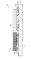
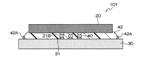
- FIG. 2 is a cross-sectional view taken along the line AA in FIG.
- FIG. 3 is a cross-sectional view taken along the line BB in FIG.
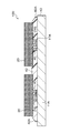
- FIG. 10 is a sectional view taken along the line CC of FIG. 9.
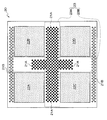
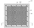
- FIG. 1 is a plan view showing a semiconductor device according to an embodiment.
- FIG. 2 is a cross-sectional view taken along the line AA in FIG. 3 is a cross-sectional view taken along the line BB of FIG.
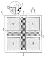
- FIG. 4 is a plan view showing a memory device chip in the semiconductor device according to the embodiment.
- the semiconductor device 100 has two memory device chips 20 (second semiconductor chips) on the same main surface of a wiring chip 10 as an interposer (mounting substrate).
- An application specific chip (Application Specific Chip: theoretical circuit chip for specific use, hereinafter referred to as ASIC: first semiconductor chip) 30 is flip-mounted.
- the two storage device chips 20 and the ASIC 30 are arranged so that one side of each of the two storage device chips 20 faces one side of the ASIC 30.
- An underfill resin 42 (sealing material) is filled between the wiring chip 10 and the storage device chip 20 and the ASIC 30.
- the underfill resin 42 protrudes on the same main surface of the wiring chip 10 and is disposed around the semiconductor chip mounting area (the mounting area of the storage device chip 20 and the ASIC 30).
- a damming member is dammed and filled.
- the dam member 42A is shown as being disposed outside the semiconductor chip mounting area, it may be disposed inside the semiconductor chip mounting area. However, the dam member 42A needs to be disposed outside the electrode group formation region.
- the wiring chip 10 is formed by arranging a plurality of metal wirings (not shown) such as aluminum wires and copper wires on a silicon substrate. 1 to 3, a connection pad 11A for mounting the storage device chip 20 and a connection pad 11B for mounting the ASIC 30 are connected to one end side and the other end side of each metal wiring. In a group. These connection pads 11A and 11B are made of a conductive material such as aluminum.
- connection pads 11A and 11B of the wiring chip 10 are arranged corresponding to the connection pads of the memory device chip 20 and the ASIC 30 to be mounted.
- the connection pads 11A and 11B of the wiring chip 10 may be arranged in a lattice pattern or a staggered pattern in the arrangement region according to the connection pads of the storage device chip 20 and the ASIC 30 to be mounted, or other arrangements. May be.
- connection pads 11A and 11B of these wiring chips 10 is appropriately set according to the chip to be mounted.
- the arrangement pitch of the connection pads 11A and 11B is 20 ⁇ m.
- the present invention is not limited to this, and can be set as appropriate within a range of 20 ⁇ m to 60 ⁇ m, for example.
- the bandwidth of the 256 Mbit multimedia memory and the ASIC 30 as the two storage device chips 20 described above will be described.
- connection pads 11A and 11B of the wiring chip 10 is also set as appropriate according to the chip to be mounted.
- the number can be appropriately set in the range of, for example, 2000 to 5000 according to the semiconductor chip to be mounted.
- the wiring chip 10 is composed of the same silicon substrate as the memory device chip 20 and the ASIC 30 to be mounted. For this reason, the physical strength with respect to heat, expansion and contraction, etc. is high, and high reliability can be secured.
- the storage device chip 20 is formed on a silicon substrate by a semiconductor process.
- a multimedia memory having a storage capacity of 256 Mbits is mounted.
- the storage device chip 20 is not limited to this, and a general-purpose dynamic random access memory (DRAM) can also be used. Similarly, a general-purpose static random access memory (SRAM), a non-volatile storage device, or the like can be used as the storage device chip 20.
- DRAM dynamic random access memory
- SRAM static random access memory
- non-volatile storage device or the like can be used as the storage device chip 20.
- the memory device chip is provided with rectangular memory banks 22A to 22D (first to fourth semiconductor circuit formation regions) divided into four on the main surface side, Storage circuits (semiconductor circuits: not shown) constituting the memories are formed in the memory banks 22A to 22D, respectively.
- the memory circuit includes, for example, a plurality of memory cells, a plurality of bit lines and a plurality of word lines connected to the plurality of memory cells, respectively, and the plurality of memories according to an address signal. And an access circuit for selecting a predetermined memory cell from the cells.
- the memory bank 22A and the memory bank 22B are arranged so that one side of the memory bank 22A and one side of the memory bank 22B face each other with a predetermined gap.
- the memory bank 22A and the memory bank 22C are arranged so that the other side orthogonal to the one side of the memory bank 22A facing the memory bank 22B and the one side of the memory bank 22C are opposed to each other with a predetermined gap.
- the memory bank 22B and the memory bank 22C are arranged so that the other side of the memory bank 22B that is orthogonal to the side facing the memory bank 22A and the one side of the memory bank 22D face each other with a predetermined gap. ing.
- the other side orthogonal to the one side facing the memory bank 22A and the other side orthogonal to the one side facing the memory bank 22B in the memory bank 22D face each other with a predetermined gap.
- a memory bank 22C and a memory bank 22D are arranged.
- four rectangular memory banks 22A to 22D are arranged on the main surface side of the storage device chip 20 so that two orthogonal sides face each other with a predetermined gap, and the entire memory banks 22A to 22D It has a shape along the edge of the main surface (the shape of the storage device chip 20: rectangular shape).
- a cross-shaped gap is provided on the main surface of the storage device chip 20 formed between the memory banks 22A to 22D opposed to each other with a predetermined gap.
- connection bump arrangement area 23 electrode arrangement area
- connection bump arrangement region 23 is composed of two orthogonal regions 23A and 23B.
- the region 23A has a gap provided between the memory banks 22A and 22B and the memory banks 22C and 22D in a direction opposite to the memory banks 22A and 22B (memory bank). 22C and 22D in the opposing direction) extending to both opposing edges of the main surface of the storage device chip 20.
- the gap provided between the memory banks 22A and 22C and the memory banks 22B and 22D is stored in the facing direction of the memory banks 22A and 22C (the facing direction of the memory banks 22B and 22D). This is an area extending to both opposing edges of the main surface of the device chip 20.
- signal input / output connection bumps 21A (first electrodes) for inputting / outputting signals of the memory device chip 20 (memory circuit) or signals to the chip are opposed to the memory banks 22A and 22B.
- a group of directions (opposing directions of the memory banks 22C and 22D) is continuously arranged.
- the arrangement of the signal input / output connection bumps 21A may be a lattice shape or a staggered shape.
- the signal input / output connection bumps 21A are provided in the region where the regions 23A and 23B intersect and overlap in the cross-shaped connection bump arrangement region 23.
- the present invention is not limited to this.
- the form which provided the connection bump 21B may be sufficient.
- power / ground connection bumps 21B (second electrodes) for supplying power to the storage device chip 20 (storage circuit) and grounding (second electrodes) are opposed to the memory banks 22A and 22C (memory bank 22B).
- 22D are arranged continuously in a group so as to extend in the opposite direction.
- the arrangement of the power / grounding connection bumps 21 ⁇ / b> B may be a lattice shape or a staggered shape.
- the signal input / output connection bumps 21A and the power / ground connection bumps 21B are arranged in the cross-shaped connection bump arrangement region 23 and are arranged in a cross-shaped connection bump group.
- the signal input / output connection bumps 21A and the power / ground connection bumps 21B are arranged in a predetermined width in each region.
- the arrangement width (number of bumps) of the signal input / output connection bumps 21A is preferably larger than the arrangement width (number of bumps) of the power / ground connection bumps 21B.
- the signal input / output connection bumps 21A (total number) provided in the region 23A are arranged in 13 (number in the width direction) ⁇ 122 (number in the longitudinal direction) and provided for the region 23B for power / grounding.
- the connection bumps 21B (total number) are arranged at 8 (number in the width direction) ⁇ 103 (number in the longitudinal direction).
- the number of bumps (number of electrodes) provided in the region 23A along the width direction is preferably 10 to 30, and the region 23B The number of bumps (number of electrodes) along the width direction is preferably 4 to 32.
- each bump (signal input / output connection bump 21A and power / ground connection bump 21B) is spaced apart from the edge of the memory bank (the edge opposite the bump) by a predetermined distance (for example, the shortest distance from the edge). At least 150 ⁇ m apart: the shortest distance is preferably indicated by t in FIG.
- a pad on which the bump is formed is disposed immediately below the signal input / output connection bump 21A (immediately below the chip thickness direction), and an input electrically connected to the pad is provided.
- a unit cell region including an output circuit is provided.
- Both the signal input / output connection bumps 21A constitute an I / O array in which unit cell regions including input / output circuits are arranged in an array.
- connection bumps signal input / output connection bumps 21A and power / ground connection bumps 21B
- connection pads 11A of the wiring chip 10 face the connection pads 11A of the wiring chip 10.
- the memory device chip 20 is arranged so that the wiring chip 10 and the electrodes (bumps, pads) face each other, are physically connected by the solder 40, and are electrically connected. Chip mounted.
- the storage device chip 20 is mounted on the wiring chip 10 so that the region 23A of the cross-shaped connection bump arrangement region 23 is parallel to the opposite side of the storage device chip 20 of the ASIC 30. Has been. Thereby, the wiring structure of the wiring chip for electrically connecting the memory device chip 20 and the wiring chip 10 is simplified, and poor connection or the like is suppressed.
- connection bump needs to be arranged on both sides in the longitudinal direction of the region 23A and the region 23B, with the center portion of the cross-shaped connection bump arrangement region 23 (the region where the region 23A and the region 23B overlap) as a center. This is preferably arranged on the subject.
- the ASIC 30 is formed on a silicon substrate by a semiconductor process, and for example, a logic circuit including a general-purpose CPU is employed.
- the storage device chip 20 includes two multi-media memories having a storage capacity of 256 Mbits, the number of input / output bits of the ASIC 30 corresponds to a bandwidth of 2.1 GB / S. 512 bits. Of course, it may be higher depending on the performance (for example, bandwidth) of the memory device chip 20.
- the ASIC 30 is not limited to this, and for example, a general-purpose analog circuit including an A / D converter that converts an analog signal into a digital signal can be used.
- connection bumps 31 are arranged in groups along the edges on opposite edges of the storage device chip 20.
- the arrangement of the power / grounding connection bumps 21 ⁇ / b> B may be a lattice shape or a staggered shape.
- the ASIC 30 is arranged so that the connection bumps 31 face the connection pads 11B of the wiring chip 10.
- the ASIC 30 is arranged so that the wiring chip 10 and the electrodes (pads, bumps) face each other, physically connected by the solder 40, and electrically connected, and mounted on the wiring chip 10 as a Philip chip. ing.
- the storage device chip 20 and the ASIC 30 are electrically and physically connected via metal wiring (not shown) connected to the connection pads of the wiring chip 10.
- the ASIC 30 is electrically connected to two 256 Mbit multi-media memories as the storage device chip 20, so that signals are input and output in parallel by 512 bits.
- connection bumps of the storage device chip 20 and the connection bumps of the ASIC 30 are electrically connected via the metal wiring (not shown) connected to the connection pads of the wiring chip 10, thereby Line connection is achieved.
- the wiring chip 10 is provided with a connection pad for external connection, and the connection wire is electrically connected, and the connection to the outside of the semiconductor device 100 is achieved by the connection wire. ing.
- the memory device chip is divided into four as regions where a memory circuit (semiconductor circuit: not shown) constituting the memory is formed on the main surface side, and orthogonal to each other.
- a memory circuit semiconductor circuit: not shown
- Four memory banks 22A to 22D having a rectangular shape are arranged such that two sides to be opposed to each other with a predetermined gap.
- a cross-shaped connection bump arrangement region 23 formed between the memory banks 22A to 22D facing each other with a predetermined gap is provided.
- the signal input / output connection bumps 21A (first electrodes) are arranged in a group in the region 23A of the cross-shaped connection bump arrangement region 23. That is, the signal input / output connection bumps 21A are unevenly distributed (aggregated), and the signal input / output wiring formation efficiency for the divided memory circuits and the chip occupation area of the electrodes are minimized.
- a group of power / grounding connection bumps 21B is disposed in a region 23B orthogonal to a region 23A in which the signal input / output connection bumps 21A form a group.
- the storage device chip 20 intersects the longitudinal direction of the group of signal input / output connection bumps 21 A of the storage device chip 20 (particularly orthogonal to the longitudinal direction).
- the power / ground connection bump 21B supports (supports via solder), and intersects the longitudinal direction of the power / ground connection bump 21B of the storage device chip 20 (particularly,
- the signal input / output connection bump 21A supports tilting in a direction perpendicular to the longitudinal direction (supported via solder).
- the memory device chip 20 is disposed with a certain gap from the wiring chip 10, that is, the opposing surfaces of the memory device chip 20 and the wiring chip 10 are in a parallel relationship.
- the gap between the memory device chip 20 and the wiring chip 10 is 20 ⁇ m to 30 ⁇ m
- the fixed distance is an error in the distance between the opposing surfaces of the memory device chip 20 and the wiring chip 10, for example, the entire chip. It means within ⁇ 3 ⁇ m to ⁇ 4 ⁇ m in the facing region.
- the parallelism when the memory device chip 20 and the wiring chip 10 are mounted is maintained with the minimum number of bumps.
- the power / ground connection bumps 21B for maintaining the parallelism are provided in the non-formation region of the memory bank, the memory circuit is caused by the pressure when the memory device chip 20 is mounted on the wiring chip 10. Is prevented from being destroyed. Since power / ground connection bumps are used as bumps (electrodes) for maintaining parallelism, electrical power / ground connection can be strengthened electrically.
- the underfill resin 42 is filled between the memory device chip 20 and the wiring chip 10, but no electrode group is interposed in the memory bank formation region of the memory device chip 20.
- the underfill resin 42 is directly filled.
- the underfill resin 42 is easily filled without a gap without causing a filling defect in the memory bank formation region.
- the underfill resin 42 sufficiently functions as a cushioning material against a physical shock, and damage to the memory bank of the memory device chip 20 due to the shock is further improved.
- the group of power / ground connection bumps 21B is arranged in a region 23B orthogonal to the region 23A in which the signal input / output connection bumps 21A form a group, that is, four rectangular memory banks. Since it is disposed in the central gap formed in 22A to 22D, the group of power / grounding connection bumps 21B is disposed at a position closest to each memory bank, and is formed in each memory bank. Power supply and grounding to the memory circuit (memory cell) are evenly and realized with the shortest wiring.
- the memory device chip 20 reduces the number of electrodes (bumps) as much as possible, maintains parallelism with the mounting substrate (wiring chip 10) during mounting, and prevents connection failure.
- the destruction of the circuit (memory circuit) can also be suppressed.
- the storage device chip continuously includes a group of power / ground connection bumps 21B as bumps (electrodes) for maintaining parallelism in the region 23B of the cross-shaped connection bump arrangement region 23.
- the present invention is not limited to this.
- the power / grounding connection bumps 21 ⁇ / b> B may be intermittently arranged in the region 23 ⁇ / b> B in the cross-shaped connection bump arrangement region 23.
- the memory device chip has a configuration in which the power / ground connection bump 21B is applied to the region 23B of the cross-shaped connection bump arrangement region 23 as a bump (electrode) for maintaining parallelism.
- a signal input / output connection bump or a dummy bump may be applied instead of the power / ground connection bump 21B.
- the signal input / output connection bump 21 ⁇ / b> A provided in the region 23 ⁇ / b> A is also continuous in the region 23 ⁇ / b> B in the cross-shaped connection bump arrangement region 23.
- the signal input / output connection bumps 21A may be arranged in a group so as to form a group.
- the signal input / output connection bumps 21A provided in the region 23B are arranged from the center of the chip to the center of the opposing region of each memory bank.
- the power / grounding connection bumps 21B are provided in groups at both ends in the longitudinal direction of the region 23B (chip both edges).
- the storage device chip 20 has been described in which four divided memory banks 22A to 22D are arranged close to the chip edge.
- the present invention is not limited to this.
- the form which provided the edge and the predetermined clearance gap may be sufficient.
- the memory banks 22A and 22B are also arranged in a similar manner so that the edge of the storage device chip 20 (one edge on the longitudinal direction side of the region 23B) has a gap.
- Each memory bank is arranged so as to have a gap between 22C and 22 and the other edge of the memory device chip 20 (the other edge in the longitudinal direction of the region 23B), and each edge is provided in both the gaps.
- the power / grounding connection bumps 21B provided in the gaps along the edges also have a predetermined distance from the edge of the memory bank (the edge facing the bumps) to the outside (for example, 150 ⁇ m at the shortest distance from the edges).
- the above-mentioned separation The shortest distance is preferably provided by being denoted by t in FIG.
- this form is the same as that shown in FIG. 6 except these.
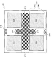
- the form in which the divided four memory banks 22A to 22D are formed has been described.
- the present invention is not limited to this.
- a set of four memory banks 22A to 22D cross-shaped connection bump arrangement region in which connection bumps are provided on the main surface of one storage device chip. 23
- two sets of these may be provided.
- two or more sets may be used.
- connection bumps are formed in the cross-shaped connection bump arrangement region 23 only on the storage device chip 20 .
- the present invention is not limited to this, and similarly, four logic circuits (semiconductor circuits) are provided. You may apply to ASIC30 divided
- the configuration in which the memory device chip 20 and the ASIC 30 are flip-mounted on the same main surface of the wiring chip 10 as an interposer (mounting substrate) has been described.
- an ASIC chip is used instead of the wiring chip 10.
- the semiconductor device may be configured by mounting so-called COC (CHIP ON CHIP). Specifically, for example, as shown in FIGS.
- a semiconductor device 101 in which the memory device chip 20 is flip-mounted on the main surface of the ASIC 30 can be cited.
- the electrode group (connection bump) of the ASIC 30 is arranged in the same arrangement as the electrode group (connection bump) of the memory device chip 20.
- connection pad 10 wiring chip 11A, 11B connection pad 20 storage device chip 21A signal input / output connection bump 21B power / ground connection bump 22A, 22B, 22C, 22D memory bank 23 connection bump arrangement area 23A, 23B area 31 connection bump 40 solder 42 Underfill resin 42A Dam member 100 Semiconductor device 101 Semiconductor device
Landscapes
- Semiconductor Integrated Circuits (AREA)
- Semiconductor Memories (AREA)
- Wire Bonding (AREA)
- Internal Circuitry In Semiconductor Integrated Circuit Devices (AREA)
Abstract
Description
請求項1に係る発明は、
半導体回路がそれぞれ形成された矩形状の4つの第1~第4の半導体回路形成領域であって、直交する2辺を所定間隙を持って互いに対向させて配設される第1~第4の半導体回路形成領域と、
互いの前記第1~第4の半導体回路形成領域間により形成される間隙からなり、且つ直交する2つの第1~第2の領域で構成される十字状の電極配置領域と、
前記十字状の電極配置領域のうち、前記第1の領域内の少なくとも一部に配設され、前記半導体回路に接続され、前記半導体回路に電力又は信号を供給する第1の電極群と、
前記十字状の電極配置領域のうち、前記第2の領域内の少なくとも一部に配設され、前記半導体回路に接続され、前記半導体回路に電力又は信号を供給する第2の電極群と、
を備える半導体チップである。
前記第1の電極群が信号入出力用の電極を含んで構成される電極群であると共に、前記第2の電極群が電力供給用の電極及び接地用の電極を含んで構成される電極群である請求項1に記載の半導体チップである。
前記半導体回路が記憶回路であると共に、前記半導体チップが記憶装置チップである請求項1又は2に記載の半導体チップである。
配線チップと、
前記配線チップの主面上に、電極群を対向させて実装された第1の半導体チップと、
前記第1の半導体チップとは異なる第2の半導体チップであって、前記配線チップの主面上に、電極群を対向させて実装された第2の半導体チップと、
を備え、
前記第2の半導体チップが、請求項1~3のいずれか1項に記載の半導体チップである半導体装置である。
第1の半導体チップと、
前記第1の半導体チップとは異なる第2の半導体チップであって、前記第1の半導体チップの主面上に、電極群を対向させて実装された第2の半導体チップと、
を備え、
前記第2の半導体チップが、請求項1~3のいずれか1項に記載の半導体チップである半導体装置である。
なお、ここで、上述した2つの記憶装置チップ20として256Mビットのマルチ・メディア・メモリとASIC30のバンド幅について説明する。前述したように、このバンド幅は、半導体装置の動作周波数と半導体装置の入出力データ数(入出力ビット数)の積として規定される。
例えば、本実施形態での半導体装置の動作周波数を33MHz、半導体装置の入出力データ数を256×2=512個とした場合、そのバンド幅は2.1GB/sとなる。
11A,11B 接続パッド
20 記憶装置チップ
21A 信号入出力用接続バンプ
21B 電力・接地用接続バンプ
22A、22B,22C、22D メモリバンク
23 接続バンプ配置領域
23A、23B 領域
31 接続バンプ
40 半田
42 アンダーフィル樹脂
42A ダム部材
100 半導体装置
101 半導体装置
Claims (5)
- 半導体回路がそれぞれ形成された矩形状の4つの第1~第4の半導体回路形成領域であって、直交する2辺を所定間隙を持って互いに対向させて配設される第1~第4の半導体回路形成領域と、
互いの前記第1~第4の半導体回路形成領域間により形成される間隙からなり、且つ直交する2つの第1~第2の領域で構成される十字状の電極配置領域と、
前記十字状の電極配置領域のうち、前記第1の領域内の少なくとも一部に配設され、前記半導体回路に接続され、前記半導体回路に電力又は信号を供給する第1の電極群と、
前記十字状の電極配置領域のうち、前記第2の領域内の少なくとも一部に配設され、前記半導体回路に接続され、前記半導体回路に電力又は信号を供給する第2の電極群と、
を備える半導体チップ。 - 前記第1の電極群が信号入出力用の電極を含んで構成される電極群であると共に、前記第2の電極群が電力供給用の電極及び接地用の電極を含んで構成される電極群である請求項1に記載の半導体チップ。
- 前記半導体回路が記憶回路であると共に、前記半導体チップが記憶装置チップである請求項1又は2に記載の半導体チップ。
- 配線チップと、
前記配線チップの主面上に、電極群を対向させて実装された第1の半導体チップと、
前記第1の半導体チップとは異なる第2の半導体チップであって、前記配線チップの主面上に、電極群を対向させて実装された第2の半導体チップと、
を備え、
前記第2の半導体チップが、請求項1~3のいずれか1項に記載の半導体チップである半導体装置。 - 第1の半導体チップと、
前記第1の半導体チップとは異なる第2の半導体チップであって、前記第1の半導体チップの主面上に、電極群を対向させて実装された第2の半導体チップと、
を備え、
前記第2の半導体チップが、請求項1~3のいずれか1項に記載の半導体チップである半導体装置。
Priority Applications (3)
| Application Number | Priority Date | Filing Date | Title |
|---|---|---|---|
| CN2009801057659A CN101952956A (zh) | 2008-02-19 | 2009-02-16 | 半导体芯片及半导体装置 |
| US12/918,401 US20100327457A1 (en) | 2008-02-19 | 2009-02-16 | Semiconductor chip and semiconductor device |
| EP09712660A EP2249381A4 (en) | 2008-02-19 | 2009-02-16 | SEMICONDUCTOR CHIP AND SEMICONDUCTOR ARRANGEMENT |
Applications Claiming Priority (2)
| Application Number | Priority Date | Filing Date | Title |
|---|---|---|---|
| JP2008037452A JP2009200101A (ja) | 2008-02-19 | 2008-02-19 | 半導体チップ及び半導体装置 |
| JP2008-037452 | 2008-02-19 |
Publications (1)
| Publication Number | Publication Date |
|---|---|
| WO2009104536A1 true WO2009104536A1 (ja) | 2009-08-27 |
Family
ID=40985417
Family Applications (1)
| Application Number | Title | Priority Date | Filing Date |
|---|---|---|---|
| PCT/JP2009/052493 Ceased WO2009104536A1 (ja) | 2008-02-19 | 2009-02-16 | 半導体チップ及び半導体装置 |
Country Status (7)
| Country | Link |
|---|---|
| US (1) | US20100327457A1 (ja) |
| EP (1) | EP2249381A4 (ja) |
| JP (1) | JP2009200101A (ja) |
| KR (1) | KR20100123860A (ja) |
| CN (1) | CN101952956A (ja) |
| TW (1) | TW201001670A (ja) |
| WO (1) | WO2009104536A1 (ja) |
Cited By (1)
| Publication number | Priority date | Publication date | Assignee | Title |
|---|---|---|---|---|
| US20230420298A1 (en) * | 2022-06-28 | 2023-12-28 | Intel Corporation | Multi-pathway routing via through hole |
Families Citing this family (38)
| Publication number | Priority date | Publication date | Assignee | Title |
|---|---|---|---|---|
| JP2009295740A (ja) * | 2008-06-04 | 2009-12-17 | Elpida Memory Inc | メモリチップ及び半導体装置 |
| JP5342422B2 (ja) * | 2009-12-10 | 2013-11-13 | ルネサスエレクトロニクス株式会社 | 半導体装置およびその製造方法 |
| US8796863B2 (en) * | 2010-02-09 | 2014-08-05 | Samsung Electronics Co., Ltd. | Semiconductor memory devices and semiconductor packages |
| US8901747B2 (en) | 2010-07-29 | 2014-12-02 | Mosys, Inc. | Semiconductor chip layout |
| KR20120056018A (ko) * | 2010-11-24 | 2012-06-01 | 삼성전자주식회사 | 범프들과 테스트 패드들이 십자 모양으로 배열되는 반도체 장치 |
| KR101262638B1 (ko) | 2010-12-06 | 2013-05-08 | 기아자동차주식회사 | 엘피아이 연료시스템용 솔레노이드 밸브 |
| JP5579108B2 (ja) | 2011-03-16 | 2014-08-27 | 株式会社東芝 | 半導体装置 |
| US8823165B2 (en) | 2011-07-12 | 2014-09-02 | Invensas Corporation | Memory module in a package |
| US8513817B2 (en) | 2011-07-12 | 2013-08-20 | Invensas Corporation | Memory module in a package |
| US8502390B2 (en) | 2011-07-12 | 2013-08-06 | Tessera, Inc. | De-skewed multi-die packages |
| US8659140B2 (en) | 2011-10-03 | 2014-02-25 | Invensas Corporation | Stub minimization using duplicate sets of signal terminals in assemblies without wirebonds to package substrate |
| KR101840240B1 (ko) * | 2011-10-03 | 2018-05-04 | 인벤사스 코포레이션 | 마이크로 전자 패키지 |
| US8659142B2 (en) | 2011-10-03 | 2014-02-25 | Invensas Corporation | Stub minimization for wirebond assemblies without windows |
| US8629545B2 (en) | 2011-10-03 | 2014-01-14 | Invensas Corporation | Stub minimization for assemblies without wirebonds to package substrate |
| TWI515864B (zh) | 2011-10-03 | 2016-01-01 | 英帆薩斯公司 | 具有自封裝中心偏移之端子格柵之短線最小化 |
| KR101894823B1 (ko) | 2011-10-03 | 2018-09-04 | 인벤사스 코포레이션 | 평행한 윈도우를 갖는 다중-다이 와이어 본드 어셈블리를 위한 스터브 최소화 |
| US8436457B2 (en) | 2011-10-03 | 2013-05-07 | Invensas Corporation | Stub minimization for multi-die wirebond assemblies with parallel windows |
| KR20140085497A (ko) | 2011-10-03 | 2014-07-07 | 인벤사스 코포레이션 | 직교 윈도가 있는 멀티-다이 와이어본드 어셈블리를 위한 스터브 최소화 |
| US8659141B2 (en) | 2011-10-03 | 2014-02-25 | Invensas Corporation | Stub minimization using duplicate sets of terminals for wirebond assemblies without windows |
| US8441111B2 (en) | 2011-10-03 | 2013-05-14 | Invensas Corporation | Stub minimization for multi-die wirebond assemblies with parallel windows |
| US8759163B2 (en) * | 2012-04-30 | 2014-06-24 | Taiwan Semiconductor Manufacturing Co., Ltd. | Layout of a MOS array edge with density gradient smoothing |
| US9006908B2 (en) * | 2012-08-01 | 2015-04-14 | Marvell Israel (M.I.S.L) Ltd. | Integrated circuit interposer and method of manufacturing the same |
| US8848392B2 (en) | 2012-08-27 | 2014-09-30 | Invensas Corporation | Co-support module and microelectronic assembly |
| US8848391B2 (en) | 2012-08-27 | 2014-09-30 | Invensas Corporation | Co-support component and microelectronic assembly |
| US8787034B2 (en) | 2012-08-27 | 2014-07-22 | Invensas Corporation | Co-support system and microelectronic assembly |
| US9368477B2 (en) | 2012-08-27 | 2016-06-14 | Invensas Corporation | Co-support circuit panel and microelectronic packages |
| US20140159238A1 (en) * | 2012-12-07 | 2014-06-12 | Qualcomm Incorporated | Package having thermal compression flip chip (tcfc) and chip with reflow bonding on lead |
| KR101324431B1 (ko) * | 2013-05-14 | 2013-10-31 | 주식회사 한국인삼공사 | 숙취해소용 조성물 |
| US9070423B2 (en) | 2013-06-11 | 2015-06-30 | Invensas Corporation | Single package dual channel memory with co-support |
| US9123555B2 (en) | 2013-10-25 | 2015-09-01 | Invensas Corporation | Co-support for XFD packaging |
| US9305131B2 (en) * | 2013-12-03 | 2016-04-05 | Mediatek Inc. | Method for flip chip packaging co-design |
| US9281296B2 (en) | 2014-07-31 | 2016-03-08 | Invensas Corporation | Die stacking techniques in BGA memory package for small footprint CPU and memory motherboard design |
| US9691437B2 (en) | 2014-09-25 | 2017-06-27 | Invensas Corporation | Compact microelectronic assembly having reduced spacing between controller and memory packages |
| US9659863B2 (en) * | 2014-12-01 | 2017-05-23 | Taiwan Semiconductor Manufacturing Company, Ltd. | Semiconductor devices, multi-die packages, and methods of manufacture thereof |
| US9543192B2 (en) * | 2015-05-18 | 2017-01-10 | Globalfoundries Singapore Pte. Ltd. | Stitched devices |
| US9484080B1 (en) | 2015-11-09 | 2016-11-01 | Invensas Corporation | High-bandwidth memory application with controlled impedance loading |
| US9679613B1 (en) | 2016-05-06 | 2017-06-13 | Invensas Corporation | TFD I/O partition for high-speed, high-density applications |
| US20230326819A1 (en) * | 2022-04-12 | 2023-10-12 | Taiwan Semiconductor Manufacturing Company Limited | Dam structure for integrated passive device integration and methods of forming the same |
Citations (9)
| Publication number | Priority date | Publication date | Assignee | Title |
|---|---|---|---|---|
| JPH07263449A (ja) | 1994-03-18 | 1995-10-13 | Hitachi Ltd | 半導体装置及びその製法 |
| JP2000188381A (ja) | 1998-12-22 | 2000-07-04 | Toshiba Corp | 半導体記憶装置 |
| JP2000315776A (ja) | 1999-05-06 | 2000-11-14 | Hitachi Ltd | 半導体装置 |
| JP2002026037A (ja) | 2000-07-05 | 2002-01-25 | Shinko Electric Ind Co Ltd | 配線基板及び半導体装置 |
| JP2003258154A (ja) | 2002-03-05 | 2003-09-12 | Fujitsu Ltd | 半導体素子の実装構造 |
| JP2004063753A (ja) * | 2002-07-29 | 2004-02-26 | Nec Kansai Ltd | チップオンチップ接続用半導体チップ及びその接続方法 |
| JP2004265940A (ja) * | 2003-02-19 | 2004-09-24 | Sony Corp | 半導体装置 |
| JP2006147629A (ja) | 2004-11-16 | 2006-06-08 | Matsushita Electric Works Ltd | 半導体装置およびその評価方法 |
| JP2007529930A (ja) | 2004-03-19 | 2007-10-25 | フォルシュングスフェアブント ベルリン エー ファウ | フリップチップ技術を用いて製造された半導体モジュールのためのマイクロ波アンテナ |
Family Cites Families (14)
| Publication number | Priority date | Publication date | Assignee | Title |
|---|---|---|---|---|
| JPH0562978A (ja) * | 1991-08-30 | 1993-03-12 | Fujitsu Ltd | フリツプチツプ |
| JP2006157047A (ja) * | 1995-03-30 | 2006-06-15 | Renesas Technology Corp | 半導体パッケージ |
| JP3494502B2 (ja) * | 1995-05-12 | 2004-02-09 | 株式会社ルネサステクノロジ | 半導体記憶装置およびそのパッド配置方法 |
| US20040061220A1 (en) * | 1996-03-22 | 2004-04-01 | Chuichi Miyazaki | Semiconductor device and manufacturing method thereof |
| US5719449A (en) * | 1996-09-30 | 1998-02-17 | Lucent Technologies Inc. | Flip-chip integrated circuit with improved testability |
| WO1998035293A1 (fr) * | 1997-02-07 | 1998-08-13 | T.I.F. Co., Ltd. | Systeme de memoire |
| JPH1131716A (ja) * | 1997-07-11 | 1999-02-02 | Hitachi Ltd | 半導体装置の製造方法及び半導体チップ |
| JP3259763B2 (ja) * | 1997-11-14 | 2002-02-25 | 日本電気株式会社 | 半導体lsi |
| JP4776861B2 (ja) * | 2002-09-26 | 2011-09-21 | ルネサスエレクトロニクス株式会社 | 半導体装置 |
| JP3722224B2 (ja) * | 2003-12-24 | 2005-11-30 | セイコーエプソン株式会社 | 半導体チップ及び半導体装置並びに半導体装置の製造方法 |
| US7015592B2 (en) * | 2004-03-19 | 2006-03-21 | Intel Corporation | Marking on underfill |
| DE102004042073A1 (de) * | 2004-08-31 | 2006-03-09 | Infineon Technologies Ag | Schaltungsanordnung zur Datenspeicherung |
| US7684781B2 (en) * | 2005-11-25 | 2010-03-23 | Semiconductor Energy Laboratory Co., Ltd | Semiconductor device |
| JP2008066371A (ja) * | 2006-09-05 | 2008-03-21 | Matsushita Electric Ind Co Ltd | 半導体集積回路における電源配線構造 |
-
2008
- 2008-02-19 JP JP2008037452A patent/JP2009200101A/ja active Pending
-
2009
- 2009-02-16 TW TW098104879A patent/TW201001670A/zh unknown
- 2009-02-16 US US12/918,401 patent/US20100327457A1/en not_active Abandoned
- 2009-02-16 WO PCT/JP2009/052493 patent/WO2009104536A1/ja not_active Ceased
- 2009-02-16 CN CN2009801057659A patent/CN101952956A/zh active Pending
- 2009-02-16 KR KR1020107019920A patent/KR20100123860A/ko not_active Ceased
- 2009-02-16 EP EP09712660A patent/EP2249381A4/en not_active Withdrawn
Patent Citations (9)
| Publication number | Priority date | Publication date | Assignee | Title |
|---|---|---|---|---|
| JPH07263449A (ja) | 1994-03-18 | 1995-10-13 | Hitachi Ltd | 半導体装置及びその製法 |
| JP2000188381A (ja) | 1998-12-22 | 2000-07-04 | Toshiba Corp | 半導体記憶装置 |
| JP2000315776A (ja) | 1999-05-06 | 2000-11-14 | Hitachi Ltd | 半導体装置 |
| JP2002026037A (ja) | 2000-07-05 | 2002-01-25 | Shinko Electric Ind Co Ltd | 配線基板及び半導体装置 |
| JP2003258154A (ja) | 2002-03-05 | 2003-09-12 | Fujitsu Ltd | 半導体素子の実装構造 |
| JP2004063753A (ja) * | 2002-07-29 | 2004-02-26 | Nec Kansai Ltd | チップオンチップ接続用半導体チップ及びその接続方法 |
| JP2004265940A (ja) * | 2003-02-19 | 2004-09-24 | Sony Corp | 半導体装置 |
| JP2007529930A (ja) | 2004-03-19 | 2007-10-25 | フォルシュングスフェアブント ベルリン エー ファウ | フリップチップ技術を用いて製造された半導体モジュールのためのマイクロ波アンテナ |
| JP2006147629A (ja) | 2004-11-16 | 2006-06-08 | Matsushita Electric Works Ltd | 半導体装置およびその評価方法 |
Non-Patent Citations (1)
| Title |
|---|
| See also references of EP2249381A4 |
Cited By (1)
| Publication number | Priority date | Publication date | Assignee | Title |
|---|---|---|---|---|
| US20230420298A1 (en) * | 2022-06-28 | 2023-12-28 | Intel Corporation | Multi-pathway routing via through hole |
Also Published As
| Publication number | Publication date |
|---|---|
| KR20100123860A (ko) | 2010-11-25 |
| EP2249381A1 (en) | 2010-11-10 |
| CN101952956A (zh) | 2011-01-19 |
| US20100327457A1 (en) | 2010-12-30 |
| JP2009200101A (ja) | 2009-09-03 |
| TW201001670A (en) | 2010-01-01 |
| EP2249381A4 (en) | 2012-11-21 |
Similar Documents
| Publication | Publication Date | Title |
|---|---|---|
| WO2009104536A1 (ja) | 半導体チップ及び半導体装置 | |
| US11894093B2 (en) | Stacked DRAM device and method of manufacture | |
| US8680652B2 (en) | Stack package | |
| TWI761632B (zh) | 包含與半導體晶粒分隔開的橋式晶粒之半導體封裝 | |
| KR102930056B1 (ko) | 관통 전극을 포함하는 반도체 칩, 및 이 반도체 칩을 포함하는 반도체 패키지 | |
| KR20200005943A (ko) | 반도체 칩 및 그 반도체 칩을 포함한 반도체 패키지 | |
| CN114121873A (zh) | 具有球栅阵列的设备和系统及相关微电子装置和装置封装 | |
| US8304879B2 (en) | Spiral staircase shaped stacked semiconductor package and method for manufacturing the same | |
| JP3774468B2 (ja) | 半導体装置 | |
| JP2015109408A (ja) | 複合チップ、半導体装置、及び半導体装置の製造方法 | |
| KR102426664B1 (ko) | 범프 패드들을 가지는 집적 회로 및 그것을 포함하는 반도체 패키지 | |
| JP3895756B1 (ja) | 半導体装置 | |
| US12532756B2 (en) | Semiconductor package, and memory module including the same | |
| JP3813768B2 (ja) | 半導体装置及び半導体モジュール | |
| JP6689420B2 (ja) | 半導体装置および半導体装置の製造方法 | |
| KR102937174B1 (ko) | 적층 패키지, 이의 제조방법 및 이를 포함하는 전자 장치 | |
| KR102891268B1 (ko) | 팬-아웃형 적층 패키지, 이의 제조방법 및 이를 포함하는 전자 장치 | |
| CN115004355A (zh) | 存储芯片堆叠封装及电子设备 | |
| JP3904587B1 (ja) | 半導体装置、及びその製造方法 | |
| CN101617404A (zh) | 半导体装置 | |
| JP2007157182A (ja) | 半導体装置 | |
| WO2014132835A1 (ja) | 半導体装置 |
Legal Events
| Date | Code | Title | Description |
|---|---|---|---|
| WWE | Wipo information: entry into national phase |
Ref document number: 200980105765.9 Country of ref document: CN |
|
| 121 | Ep: the epo has been informed by wipo that ep was designated in this application |
Ref document number: 09712660 Country of ref document: EP Kind code of ref document: A1 |
|
| WWE | Wipo information: entry into national phase |
Ref document number: 12918401 Country of ref document: US |
|
| NENP | Non-entry into the national phase |
Ref country code: DE |
|
| ENP | Entry into the national phase |
Ref document number: 20107019920 Country of ref document: KR Kind code of ref document: A |
|
| WWE | Wipo information: entry into national phase |
Ref document number: 2009712660 Country of ref document: EP |