WO2009107517A1 - 薄膜太陽電池およびその製造方法 - Google Patents
薄膜太陽電池およびその製造方法 Download PDFInfo
- Publication number
- WO2009107517A1 WO2009107517A1 PCT/JP2009/052686 JP2009052686W WO2009107517A1 WO 2009107517 A1 WO2009107517 A1 WO 2009107517A1 JP 2009052686 W JP2009052686 W JP 2009052686W WO 2009107517 A1 WO2009107517 A1 WO 2009107517A1
- Authority
- WO
- WIPO (PCT)
- Prior art keywords
- thin film
- solar cell
- film solar
- photoelectric conversion
- electrode layer
- Prior art date
- Legal status (The legal status is an assumption and is not a legal conclusion. Google has not performed a legal analysis and makes no representation as to the accuracy of the status listed.)
- Ceased
Links
Images

Classifications
-
- H—ELECTRICITY
- H10—SEMICONDUCTOR DEVICES; ELECTRIC SOLID-STATE DEVICES NOT OTHERWISE PROVIDED FOR
- H10F—INORGANIC SEMICONDUCTOR DEVICES SENSITIVE TO INFRARED RADIATION, LIGHT, ELECTROMAGNETIC RADIATION OF SHORTER WAVELENGTH OR CORPUSCULAR RADIATION
- H10F71/00—Manufacture or treatment of devices covered by this subclass
-
- H—ELECTRICITY
- H10—SEMICONDUCTOR DEVICES; ELECTRIC SOLID-STATE DEVICES NOT OTHERWISE PROVIDED FOR
- H10F—INORGANIC SEMICONDUCTOR DEVICES SENSITIVE TO INFRARED RADIATION, LIGHT, ELECTROMAGNETIC RADIATION OF SHORTER WAVELENGTH OR CORPUSCULAR RADIATION
- H10F19/00—Integrated devices, or assemblies of multiple devices, comprising at least one photovoltaic cell covered by group H10F10/00, e.g. photovoltaic modules
- H10F19/30—Integrated devices, or assemblies of multiple devices, comprising at least one photovoltaic cell covered by group H10F10/00, e.g. photovoltaic modules comprising thin-film photovoltaic cells
- H10F19/31—Integrated devices, or assemblies of multiple devices, comprising at least one photovoltaic cell covered by group H10F10/00, e.g. photovoltaic modules comprising thin-film photovoltaic cells having multiple laterally adjacent thin-film photovoltaic cells deposited on the same substrate
-
- H—ELECTRICITY
- H10—SEMICONDUCTOR DEVICES; ELECTRIC SOLID-STATE DEVICES NOT OTHERWISE PROVIDED FOR
- H10F—INORGANIC SEMICONDUCTOR DEVICES SENSITIVE TO INFRARED RADIATION, LIGHT, ELECTROMAGNETIC RADIATION OF SHORTER WAVELENGTH OR CORPUSCULAR RADIATION
- H10F19/00—Integrated devices, or assemblies of multiple devices, comprising at least one photovoltaic cell covered by group H10F10/00, e.g. photovoltaic modules
- H10F19/30—Integrated devices, or assemblies of multiple devices, comprising at least one photovoltaic cell covered by group H10F10/00, e.g. photovoltaic modules comprising thin-film photovoltaic cells
- H10F19/31—Integrated devices, or assemblies of multiple devices, comprising at least one photovoltaic cell covered by group H10F10/00, e.g. photovoltaic modules comprising thin-film photovoltaic cells having multiple laterally adjacent thin-film photovoltaic cells deposited on the same substrate
- H10F19/33—Patterning processes to connect the photovoltaic cells, e.g. laser cutting of conductive or active layers
-
- H—ELECTRICITY
- H10—SEMICONDUCTOR DEVICES; ELECTRIC SOLID-STATE DEVICES NOT OTHERWISE PROVIDED FOR
- H10F—INORGANIC SEMICONDUCTOR DEVICES SENSITIVE TO INFRARED RADIATION, LIGHT, ELECTROMAGNETIC RADIATION OF SHORTER WAVELENGTH OR CORPUSCULAR RADIATION
- H10F19/00—Integrated devices, or assemblies of multiple devices, comprising at least one photovoltaic cell covered by group H10F10/00, e.g. photovoltaic modules
- H10F19/80—Encapsulations or containers for integrated devices, or assemblies of multiple devices, having photovoltaic cells
-
- Y—GENERAL TAGGING OF NEW TECHNOLOGICAL DEVELOPMENTS; GENERAL TAGGING OF CROSS-SECTIONAL TECHNOLOGIES SPANNING OVER SEVERAL SECTIONS OF THE IPC; TECHNICAL SUBJECTS COVERED BY FORMER USPC CROSS-REFERENCE ART COLLECTIONS [XRACs] AND DIGESTS
- Y02—TECHNOLOGIES OR APPLICATIONS FOR MITIGATION OR ADAPTATION AGAINST CLIMATE CHANGE
- Y02E—REDUCTION OF GREENHOUSE GAS [GHG] EMISSIONS, RELATED TO ENERGY GENERATION, TRANSMISSION OR DISTRIBUTION
- Y02E10/00—Energy generation through renewable energy sources
- Y02E10/50—Photovoltaic [PV] energy
Definitions
- the present invention relates to a thin-film solar cell with improved insulation voltage resistance and a method for manufacturing the same.
- Patent Document 1 discloses that a plurality of thin film photoelectric conversion elements in which a transparent electrode layer, a photoelectric conversion layer, and a metal electrode layer are sequentially laminated on the surface of a light-transmitting insulating substrate are electrically connected to each other.
- a thin film solar cell with strings connected in series is disclosed.
- This thin-film solar cell has a structure in which the entire surface of a translucent insulating substrate including strings is sealed with a resin layer and a protective film.
- the thin film solar cell of Patent Document 1 has an insulating separation line having a width of about 0.5 mm to 1 cm at a position away from the outer peripheral end face of the translucent insulating substrate by a predetermined dimension inward.
- the insulating separation line is obtained by removing the transparent electrode layer, the photoelectric conversion layer, and the metal electrode layer (hereinafter sometimes referred to as a conductive film), and the necessary insulation withstand voltage is ensured by the insulating separation line.
- a method of forming the insulating separation line a method of removing the conductive film using a laser beam, a polishing machine, or spraying of fine particles has been proposed.
- the insulating separation line is mechanically formed by a polishing method using a polishing machine or a blasting method in which fine particles are sprayed
- the conductive film is mechanically removed. It is not a processing method.
- polishing scraps, abrasive grains, fine particles, and the like adhere to the string surface after processing, a water cleaning step is required, and further, the water used for cleaning is also required, which increases the manufacturing process and cost.
- a method of removing the conductive film by chemical etching is also conceivable, but in the case of such a wet process, in addition to the addition of a cleaning process, management of chemical concentration, temperature, etc. Since this is necessary, the processing apparatus becomes complicated, resulting in an increase in cost, which is not preferable.
- the inventors removed the conductive film by laser processing and conducted an experiment to evaluate the insulation voltage resistance with an insulation test apparatus before sealing the thin film solar cell. It became clear. When this insulation failure was analyzed, conductive processing dust generated during laser processing and seizures of this conductive processing dust adhered to the exposed transparent insulating substrate surface in the insulation separation line. It was found that insulation failure occurred. Moreover, when the applied voltage in the dielectric strength test increases as the system voltage of the thin film solar cell increases, the problem of insulation failure becomes significant.
- An object of the present invention is to solve such problems of the prior art and provide a highly reliable thin-film solar cell that secures necessary dielectric strength with a simple method and a method for manufacturing the same.
- a plurality of thin film photoelectric conversion elements in which the first electrode layer, the photoelectric conversion layer, and the second electrode layer are sequentially stacked on the surface of the translucent insulating substrate are electrically connected in series with each other.
- a string forming step for forming a string, and a film removal for forming a non-conductive surface region on the entire periphery by removing the thin film photoelectric conversion element portion formed on the outer periphery of the surface of the translucent insulating substrate with a light beam There is provided a method of manufacturing a thin-film solar cell including a step and a cleaning step of removing conductive deposits generated in the film removal step and adhered to the non-conductive surface region.
- the thin-film solar cell manufactured by the method for manufacturing the thin-film solar cell, the string formed on the surface of the translucent insulating substrate, and the translucent insulation The non-conductive surface region formed on the outer peripheral portion of the surface of the substrate, and the non-conductive surface region has a width equal to or greater than the width corresponding to the system voltage from the end surface of the outer peripheral portion of the translucent insulating substrate to the inside.
- a thin film solar cell is provided.
- the first electrode layer, the photoelectric conversion layer, and the second electrode layer removed by the light beam are formed as conductive deposits on the nonconductive surface region. Even if it adheres, the deposit can be reliably removed by cleaning the non-conductive surface region. As a result, a thin film solar cell with improved insulation voltage resistance can be obtained with a high yield.
- FIG. 2 is a sectional view taken along line AA in FIG. 1.
- FIG. 2 is a sectional view taken along line BB in FIG. It is a top view which shows Embodiment 2 of the thin film solar cell of this invention.
- FIG. 5 is a cross-sectional view taken along the line CC of FIG.
- a plurality of thin film photoelectric conversion elements in which a first electrode layer, a photoelectric conversion layer, and a second electrode layer are sequentially laminated on the surface of a light-transmitting insulating substrate are electrically connected in series.
- a string forming step for forming connected strings, and a thin film photoelectric conversion element portion formed on the outer peripheral portion of the surface of the translucent insulating substrate is removed by a light beam to form a non-conductive surface region on the entire periphery.
- a cleaning process for removing conductive deposits generated in the film removing process and adhered to the non-conductive surface region.
- the conductive deposit is a thin film photoelectric conversion element portion (first electrode layer, formed on the outer peripheral portion of the surface of the translucent insulating substrate by irradiating a light beam in the film removing step.
- At least one of the burned-in conductive baking products is included.
- the thin film photoelectric conversion element portion may be referred to as an element
- the thin film photoelectric conversion element portion to be removed may be referred to as a conductive film.
- a thin film solar cell having a desired dielectric strength can be manufactured with a high yield by removing and cleaning conductive deposits adhered to a non-conductive surface region.
- the formation of the non-conductive surface region by the light beam irradiation is performed by translating the light beam irradiation to form a plurality of grooves, so that the above-mentioned deposits are avoided in this step.
- withstand voltage resistance means that even if a predetermined high voltage is applied between the frame attached to the outer periphery of the thin film solar cell and the thin film solar cell, no discharge occurs between the frame and the thin film solar cell. Means a characteristic.
- the insulation voltage resistance for example, it can be checked whether a predetermined insulation voltage resistance is obtained by an insulation withstand voltage test defined by international standards (IEC: 61730 and 61646). In the case of a thin film solar cell module with a system voltage of 1000 V, the international standard requires an insulation withstand voltage against a lightning surge withstand voltage of 6 KV.
- the thin-film solar cell after the wiping step may include an inspection step for checking whether the thin film solar cell has a desired withstand voltage.
- This inspection process is performed for each thin film solar cell, and a predetermined voltage is applied to the outer peripheral end face of the translucent insulating substrate with the second electrode layer grounded, and the resistance value is equal to or greater than a predetermined value (current value). Is determined to be acceptable.
- the applied voltage is set to a voltage corresponding to the system voltage of the thin film solar cell. For example, in the case of a thin film solar cell with a system voltage of 1000 V, a voltage of 6000 V is applied, and if the current value is less than 50 ⁇ A, it is determined to be acceptable. .
- the cleaning process may be performed by an operator (human power) or mechanically, but in any case, the deposits present in the non-conductive surface region cannot be completely removed. It is desirable to assume a case in which the resistance value remains below a predetermined value in the inspection process. Therefore, in the present invention, when the resistance value in the first inspection process is less than a predetermined value (the current value exceeds a predetermined value), the cleaning process and the inspection process may be repeated once or more in this order. In this way, the problem that the resistance value becomes less than the predetermined value due to the remaining deposits can be made almost zero, the insulation withstand voltage required by the thin film solar cell is further improved, and the yield is increased to 100. %.
- a thin-film solar cell can be obtained by identifying a defective portion of insulation in the non-conductive surface region by visual inspection or the like, subjecting only that portion to mechanical polishing and insulating treatment, and passing the insulation test again. There is no need to dispose of it.
- the means for the cleaning step is not particularly limited as long as the conductive deposits present in the non-conductive surface region can be removed without damaging the thin film solar cell.
- a method of wiping off deposits on the non-conductive surface area using a wiping material a method of blowing air to blow off deposits on the non-conductive surface area, and deposits on the non-conductive surface area together with air Examples include a method of sucking, and these may be combined.
- it is preferable that at least a removal method using a wiping material is included from the viewpoint of effectively removing a conductive seizure that is harder to remove than conductive processing dust.
- the wiping material a material obtained by soaking a wiping base material that does not damage the light-transmitting insulating substrate and the second electrode layer exposed to the outside during wiping is used. Can do. Even conductive seizures (deposits) burned onto the non-conductive surface area were peeled off from the non-conductive surface area by physical action due to friction with the wiping substrate and wetted by the organic solvent. The deposits are wiped off without reattaching on the wiping substrate.
- a wiping substrate cloth, non-woven fabric or sponge is suitable.
- an organic solvent the highly volatile thing which volatilizes from a nonelectroconductive surface area immediately after wiping off is preferable, for example, ethanol, acetone, etc. are suitable. By using a highly volatile organic solvent, it is difficult for the organic solvent liquid to remain in the non-conductive surface region subjected to the wiping treatment, and the inspection reliability in the next inspection step can be further increased.
- a thin-film solar cell obtained by this manufacturing method includes a string formed on the surface of a light-transmitting insulating substrate and a non-conductive surface region formed on the outer peripheral portion of the surface of the light-transmitting insulating substrate.
- the transparent surface region is formed with a width equal to or larger than the width corresponding to the system voltage from the end surface of the outer peripheral portion of the translucent insulating substrate to the inside.
- the width of the non-conductive surface region is, for example, required to be 6.4 mm or more when the system voltage of the thin-film solar cell is 301 to 600 V, and 8.4 mm or more when the system voltage is 601 to 1000 V (IEC: 61730 and 61646). It is prescribed by.
- the adhering material adheres or seizes to the end surface portion of each thin film photoelectric conversion element adjacent to the non-conductive surface region, and these remain without being wiped off.
- the electrode layer and the second electrode layer are short-circuited by the deposit, and the element does not generate power.
- the power generation cell may be destroyed by the wiping operation.
- an element that may not generate power due to a short circuit among the plurality of elements is an element other than elements positioned at both ends in the element series connection direction. Of the elements located at both ends in the series connection direction, the element on the current extraction side does not contribute to power generation.
- the thin film photoelectric conversion elements are arranged at a position 0.5 to 10 mm away from the boundary between the non-conductive surface region and the string positioned in the direction orthogonal to the series connection direction.
- An insulating separation line from which the conversion element portion (conductive film including the first electrode layer, the photoelectric conversion layer, and the second electrode layer) is removed may be further formed with a width of about 10 to 300 ⁇ m.
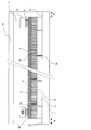
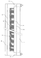
- FIG. 1 is a plan view showing Embodiment 1 of the thin-film solar cell of the present invention
- FIG. 2 is a cross-sectional view taken along the line AA in FIG. 1
- FIG. 3 is a cross-sectional view taken along the line BB in FIG.
- This thin film solar cell includes a rectangular translucent insulating substrate 1 and a thin film photoelectric substrate in which a first electrode layer 2, a photoelectric conversion layer 3, and a second electrode layer 4 are sequentially laminated on the surface of the translucent insulating substrate 1.
- This is a super straight type thin film solar cell including a string S1 in which a plurality of conversion elements 5 are electrically connected in series with each other.
- Translucent insulating substrate and first electrode layer As the translucent insulating substrate 1, a glass substrate having heat resistance and translucency in the subsequent film forming process, a resin substrate such as polyimide, and the like can be used.
- the first electrode layer 2 is made of a transparent conductive film, and is preferably made of a transparent conductive film made of a material containing ZnO or SnO 2 .
- the material containing SnO 2 may be SnO 2 itself or a mixture of SnO 2 and another oxide (for example, ITO which is a mixture of SnO 2 and In 2 O 3 ).
- each semiconductor layer forming the photoelectric conversion layer 3 is not particularly limited, for example, made of silicon-based semiconductor, CIS (CuInSe 2) compound semiconductor, CIGS (Cu (In, Ga ) Se 2) compound semiconductor or the like.
- CIS CuInSe 2 compound semiconductor
- CIGS Cu (In, Ga ) Se 2 compound semiconductor or the like.
- Sicon-based semiconductor means amorphous or microcrystalline silicon, or a semiconductor in which carbon, germanium, or other impurities are added to amorphous or microcrystalline silicon (silicon carbide, silicon germanium, or the like).
- microcrystalline silicon means silicon in a mixed phase state of crystalline silicon having a small crystal grain size (about several tens to thousands of thousands) and amorphous silicon. Microcrystalline silicon is formed, for example, when a crystalline silicon thin film is manufactured at a low temperature using a non-equilibrium process such as a plasma CVD method.
- the photoelectric conversion layer 3 is formed by laminating a p-type semiconductor layer, an i-type semiconductor layer, and an n-type semiconductor layer in order from the first electrode 2 side.
- the p-type semiconductor layer is doped with p-type impurity atoms such as boron and aluminum
- the n-type semiconductor layer is doped with n-type impurity atoms such as phosphorus.
- the i-type semiconductor layer may be a completely non-doped semiconductor layer, or may be a weak p-type or weak n-type semiconductor layer having a small amount of impurities and sufficiently equipped with a photoelectric conversion function.
- amorphous layer” and “microcrystalline layer” mean amorphous and microcrystalline semiconductor layers, respectively.
- the photoelectric conversion layer 3 may be a tandem type in which a plurality of pin structures are stacked.
- an a-Si: Hp layer, an a-Si: Hi layer, and an a-Si: Hn layer are formed on the first electrode 2.
- the upper semiconductor layer may be sequentially stacked, and the lower semiconductor layer may be formed by stacking a ⁇ c-Si: Hp layer, a ⁇ c-Si: Hi layer, and a ⁇ c-Si: Hn layer in this order on the upper semiconductor layer.
- the pin structure may be a photoelectric conversion layer 3 having a three-layer structure including an upper semiconductor layer, a middle semiconductor layer, and a lower semiconductor layer.
- amorphous silicon (a-Si) is used for the upper and middle semiconductor layers, and lower semiconductor layers are used.
- a three-layer structure using microcrystalline silicon ( ⁇ c-Si) may be used.
- the combination of the material and laminated structure of the photoelectric conversion layer 3 is not particularly limited.
- the semiconductor layer located on the light incident side of the thin-film solar cell is the upper semiconductor layer, and the semiconductor layer located on the opposite side to the light incident side is the lower semiconductor layer.
- the configuration and material of the second electrode layer 4 are not particularly limited, but in one example, the second electrode 4 has a stacked structure in which a transparent conductive film and a metal film are stacked on the photoelectric conversion layer.
- the transparent conductive film is made of ZnO, ITO, SnO 2 or the like.
- the metal film is made of a metal such as silver or aluminum.
- the second electrode layer 4 may be made of only a metal film such as Ag or Al.
- the transparent conductive film such as ZnO, ITO or SnO 2 is disposed on the photoelectric conversion layer 3 side, the second electrode layer 4 is absorbed by the photoelectric conversion layer 3.
- the reflectance which reflects the light which did not exist in the back electrode layer 4 improves, and it is preferable at the point which can obtain the thin film solar cell of high conversion efficiency.
- the string S1 has a plurality of separation grooves 7 formed on the surface.
- the plurality of separation grooves 7 electrically connect the second electrode 4 and the photoelectric conversion layer 3 of one thin film photoelectric conversion element 5 to the second electrode 4 and the photoelectric conversion layer 3 of another adjacent thin film photoelectric conversion element 5.
- the laminated film 5a including the first electrode, the photoelectric conversion layer, and the second electrode at one end (left end in FIG. 2) in the element series connection direction of the string S1 is substantially formed because the width in the series connection direction is narrow. It does not contribute to power generation.
- the second electrode of the laminated film 5a is used as the extraction electrode 4a of the first electrode 2 of the adjacent thin film photoelectric conversion layer 5. Further, as shown in FIG. 3, in order to prevent leakage due to the above-mentioned deposits adhering to the element end face, the photoelectric conversion layer 13 and the second electrode layer 14 at both ends in the longitudinal direction of each element 5 are connected to the first electrode layer 12. It cuts inward than.
- the string S1 is formed on the inner side of the outer peripheral end face (end face of the four sides) of the translucent insulating substrate 1. That is, the outer peripheral region of the surface of the translucent insulating substrate 1 is a non-conductive surface region 8 to which the first electrode layer 2, the photoelectric conversion layer 3, and the second electrode layer 4 are not attached.
- the non-conductive surface region 8 is formed by removing the first electrode layer 2, the photoelectric conversion layer 3 and the second electrode layer 4 existing on the outer periphery of the substrate during the formation of the string S1, and the non-conductive surface This is an insulating region in which the above-mentioned deposits generated when the region 8 is formed are removed and cleaned.
- the width W of the nonconductive surface region 8 is set to a dimension range corresponding to the output voltage of the thin film solar cell.
- the bus bar 10 On the second electrode 4 and the extraction electrode 4a located at both ends of the string S1 in the element series connection direction, the bus bar 10 is electrically connected by a brazing material 9 (for example, silver paste) along the longitudinal direction thereof. Has been. Each bus bar 10 is electrically connected to an unillustrated take-out line (for example, a copper wire).
- a back surface sealing material 18 is laminated on the translucent insulating substrate 1 with an adhesive layer 17 so as to completely cover the string S1 and the nonconductive surface region 8.
- the adhesive layer 17 for example, a sealing resin sheet made of ethylene-vinyl acetate copolymer (EVA) can be used.
- the back surface sealing material 18 for example, a laminated film of PET / aluminum / PET can be used.
- the adhesive layer 17 and the back surface sealing material 18 are previously formed with small holes for leading the leading ends of the respective extraction lines to the outside.
- a terminal box having an output line and a terminal electrically connected to each take-out line is attached on the back surface sealing material 18.
- a frame (for example, made of aluminum) is attached to the outer peripheral portion of the thin film solar cell sealed with the back surface sealing material 18 and the adhesive layer 17.
- a plurality of thin film photoelectric conversion elements 5 in which the first electrode layer 2, the photoelectric conversion layer 3, and the second electrode layer 4 are sequentially stacked on the surface of the light-transmitting insulating substrate 1 are electrically connected to each other.
- a string forming step for forming the string S1 connected in series, and a thin film photoelectric conversion element portion formed on the outer peripheral portion of the surface of the translucent insulating substrate 1 are removed by a light beam to completely remove the non-conductive surface region 8.
- a non-conductive surface region that is preferably cleaned, including at least a film-removing step formed around the periphery and a cleaning step that removes conductive deposits generated in the film-removing step and attached to the non-conductive surface region 8 8 can be manufactured by a method for manufacturing a thin-film solar cell including an inspection step for inspecting the insulating property.
- a transparent conductive film having a film thickness of 600 to 1000 nm is formed on the entire surface of the translucent insulating substrate 1 by a method such as CVD, sputtering, or vapor deposition, and the transparent conductive film is partially irradiated with a light beam.
- the first electrode layer 2 having a predetermined pattern is formed by forming the separation line 2a by removing.
- the transparent conductive film is separated into strips with a predetermined width, and separation lines 2a are formed at predetermined intervals.
- the leftmost first electrode layer 2 is a portion that does not function as an element, and thus has a narrow width.
- an upper semiconductor layer is formed by laminating an a-Si: Hp layer, an a-Si: Hi layer (film thickness of about 150 nm to 300 nm), and an a-Si: Hn layer in this order on the first electrode 2.
- a lower semiconductor layer is formed by laminating a ⁇ c-Si: Hp layer, a ⁇ c-Si: Hi layer (film thickness of about 1.5 ⁇ m to 3 ⁇ m), and a ⁇ c-Si: Hn layer in this order on the semiconductor layer.
- the photoelectric conversion layer 3 having a predetermined pattern is formed by partially removing the photoelectric conversion film having a tandem structure with a light beam to form the contact line 3a.
- the photoelectric conversion film is separated into strips with a predetermined width, and the first electrode layer 2 and the second electrode layer 2 are separated from each other.
- a contact line 3a for electrically connecting the electrode layer 4 is formed.
- a YVO 4 laser (wavelength: 532 nm) may be used as the laser instead of the second harmonic of the YAG laser.
- a conductive film is formed on the photoelectric conversion layer 3 so as to completely embed the contact line 3a by a method such as CVD, sputtering, or vapor deposition, and the conductive film and the photoelectric conversion layer 3 are partially removed by a light beam.
- the separation line 7 the second electrode layer 4 having a predetermined pattern is formed.
- a string in which a plurality of thin film photoelectric conversion elements 5 are connected in series on the translucent insulating substrate 1 is formed.
- the conductive film can have a two-layer structure of a transparent conductive film (ZnO, ITO, SnO 2 or the like) and a metal film (Ag, Al, or the like).
- the thickness of the transparent conductive film can be 10 to 100 nm, and the thickness of the metal film can be 100 to 500 nm.
- the second harmonic of the YAG laser or the second harmonic of the YVO 4 laser having high transparency to the first conductive layer 2 is used.
- the conductive film is separated into strips with a predetermined width, and a separation line 7 is formed. At this time, it is preferable to select a processing condition that minimizes damage to the first electrode layer 2 and suppresses the generation of burrs of the silver electrode after processing the second electrode layer 4.
- the first electrode layer 2 which is a thin film photoelectric conversion element portion formed on the outer peripheral portion of the surface of the translucent insulating substrate 1 with a predetermined width inward from the outer peripheral end surface of the translucent insulating substrate 1;
- the photoelectric conversion layer 3 and the second electrode layer 4 are removed using the fundamental wave of the YAG laser, and the non-conductive surface region 8 is formed all around.
- the string S1 surrounded by the non-conductive surface region 8 is formed.
- the processing width of the laser beam is preferably 150 to 1500 ⁇ m, more preferably 400 to 1000 ⁇ m.
- the beam distribution has a shape close to a rectangular distribution with respect to the processing direction and the processing width direction. In this way, the workability is improved as compared to the Gaussian distribution beam profile, so that the overlap of the beams can be reduced, the number of laser processing is reduced, and the apparatus can be tact-uped.
- the thin-film solar cell is set in a dielectric strength test apparatus, a predetermined voltage is applied to the outer peripheral end face of the translucent insulating substrate 1 with the extraction electrode of the second electrode layer 4 grounded, and the current value Is determined to be acceptable if the value is equal to or less than a predetermined value (50 ⁇ A). If the result of the inspection is acceptable, the process proceeds to the next process. If the result is unacceptable, the cleaning process and the inspection process are repeated once or twice. In addition, the cleaning process and the inspection process were repeated twice because it was rejected. If the test was still unsuccessful, the thin film solar cell was judged to be poorly insulated and ejected from the line. A repair process is performed to confirm and mechanically polish only defective parts.
- a silver paste 9 is applied onto the second electrode layer 4 at both ends in the element series direction of the thin film solar cell that has passed the inspection process, the bus bar 10 is pressure-bonded to the silver paste 9, and the bus bar 10 is electrically connected to the second electrode layer 4. Are connected to produce a current extraction portion.
- a transparent EVA sheet as the adhesive layer 17 and the back surface sealing material 18 are stacked on the back surface side (non-light-receiving surface side) of the thin film solar cell, and the back surface through the adhesive layer 17 using a vacuum laminator.
- the sealing material 18 is bonded and sealed to the thin film solar cell. At this time, it is preferable to use a laminated film of PET / Al / PET as the back surface sealing material 18.
- the lead-out line is electrically connected to the output line of the terminal box, the terminal box is bonded to the back surface sealing material 18, and the inside of the terminal box is filled with silicone resin.
- an aluminum frame is attached to the outer peripheral part of a thin film solar cell, and commercialization is completed. Thereafter, a predetermined voltage is applied to the aluminum frame while the second electrode layer 4 is grounded, and it is confirmed that the current value is not more than the predetermined value.
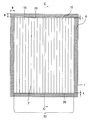
- FIG. 4 is a plan view showing Embodiment 2 of the thin film solar cell of the present invention
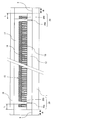
- FIG. 5 is a cross-sectional view taken along the line CC of FIG. 4 and 5, the same components as those in FIGS. 1 and 3 are denoted by the same reference numerals.
- the difference between the second embodiment and the first embodiment is that the boundary between the non-conductive surface region 8 and the string S2 in which the plurality of thin film photoelectric conversion elements 15 are located in a direction (element longitudinal direction) perpendicular to the direction of series connection.
- the insulating separation line 20 having a width of 100 to 300 ⁇ m is formed by removing the first electrode layer 12, the photoelectric conversion layer 13, and the second electrode layer 14 at a position away from the inside by a predetermined distance L. .
- the thin-film solar cell of Embodiment 2 has basically the same configuration as the thin-film solar cell of Embodiment 1 except that it has an insulation separation line 20.
- the distance L preferably has a dimension that leaves the power generation region of the string S1 as wide as possible and can easily form the insulating separation line 20 with a light beam, specifically about 0.5 to 10 mm.
- the insulating separation line 20 includes a first groove 20a having a narrow width (about 30 to 100 ⁇ m) formed in the first electrode layer 12 portion and a thick width (in the photoelectric conversion layer 13 portion and the second electrode layer 14 portion).
- the width of the insulating separation line 20 is the width of the second groove 20b.
- the distance L is a distance from the boundary between the nonconductive surface region 8 and the string S2 to the second groove 20b in the insulating separation line 20.
- the first electrode layer 12 and the second electrode layer facing the non-conductive surface region 8 as described above are obtained by separating the both end portions in the direction orthogonal to the series connection direction of the strings S1 by the insulating separation line 20 as described above. Even when 14 is electrically connected to the conductive deposit, it is possible to prevent a problem that an element corresponding to that portion does not generate power due to a short circuit.
- the insulation separation lines 20 are also formed in the elements located at both ends in the series connection direction. However, the insulation separation lines 20 may not be formed in the elements at both ends. .
- the manufacturing method of the second embodiment is the same as that of the first embodiment except that the film removal step of the first embodiment includes a step of forming the insulating separation line 20.
- the first electrode layer 12, the photoelectric conversion layer 13, and the second electrode layer 14 are removed by the fundamental wave of the YAG laser to form the first groove 20a, and then the electric conversion on both sides thereof is performed.
- the layer 13 and the second electrode layer 14 are removed by the second harmonic to form the second groove 20b.
- the photoelectric conversion layer 13 and the second electrode layer 14 are removed by the second harmonic to form the second groove 20b, and then the first electrode layer 12 in the groove is removed by the fundamental wave of the YAG laser.
- the groove 20a is formed.
- the processing waste of the first electrode layer 12 becomes the first electrode layer 12 and the second electrode.
- the problem is that the layer 14 is bridged to cause a short circuit, or the end face of the photoelectric conversion layer 13 is crystallized by the energy of the laser and the electrical conductivity increases to cause the first electrode layer 12 and the second electrode layer 14 to be in a short circuit state.
- the second groove 20b is made wider than the first groove 20a to make the groove width different, thereby preventing a short circuit.
- Example 1 10,000 thin-film solar cells having the structure of Embodiment 1 described with reference to FIGS. 1 to 3 were manufactured under conditions corresponding to a system voltage of 1000V.
- the first electrode 2 was formed by patterning using waves.
- the obtained substrate is ultrasonically cleaned with pure water, and then an upper semiconductor layer comprising an a-Si: Hp layer, an a-Si: Hi layer (film thickness of about 200 nm), and an a-Si: Hn layer;
- a photoelectric conversion film was formed by forming a lower semiconductor layer composed of a ⁇ c-Si: Hp layer, a ⁇ c-Si: Hi layer (film thickness of about 2 ⁇ m), and a ⁇ c-Si: Hn layer.
- the photoelectric conversion layer 3 was formed by patterning the photoelectric conversion film using the second harmonic of the YAG laser.
- a separation line 7 is formed using the second harmonic of a YAG laser, etc.
- a second electrode layer 4 having a pattern was formed.
- the first electrode layer 2, the photoelectric conversion layer 3, and the second electrode layer 4 on the outer peripheral portion of the string S1 were removed using a fundamental wave of a YAG laser to form a nonconductive surface region 8 having a width of 10 mm.
- the non-conductive surface region 8 was wiped using a wiping material obtained by dropping ethanol on the nonwoven fabric.
- the obtained thin film solar cell was set in an insulation test apparatus, 6000 V was applied to the translucent insulating substrate 1 with the second electrode layer 4 grounded, and the current value was measured. And about 10,000 thin-film solar cells of Example 1, the pass rate with an electric current value of 50 micrometers or less was investigated, and the result was shown in Table 1.
- Example 1 300 thin-film solar cells were produced as Comparative Example 1 in the same manner as in Example 1 except that the non-conductive surface region was not wiped off. The values were measured and the pass rate with a current value of 50 ⁇ m or less was examined. The results are shown in Table 1.
- Example 1 From the results of Table 1, in Example 1, a non-conductive surface region was cleaned using a wiping material, and a pass rate of almost 100% was obtained, but in Comparative Example 1 in which the wiping step was omitted. It was found that the acceptance rate dropped significantly. Therefore, in the film removal step for forming the nonconductive surface region, the first electrode layer, the photoelectric conversion layer, and the second electrode layer removed by the light beam adhere to the nonconductive surface region as conductive deposits. It was confirmed that this deposit reduced the insulation voltage resistance of the thin-film solar cell, and that the removal of the deposit was very effective while wiping with a wiping material was simple.
- Example 2 10000 thin-film solar cells of Example 1 were attached to an aluminum frame to produce a product, and these were also tested using the insulation test apparatus, applying 6000 V to the aluminum frame with the second electrode layer 4 grounded, and having a resistance value. It was measured. And about 10,000 thin-film solar cells of Example 2, when the pass rate with an electric current value of 50 micrometers or less was investigated, the pass rate was 99.98%.
- Example 3 In accordance with Example 1, 1000 thin-film solar cells having the structure of Embodiment 2 described with reference to FIGS. 4 and 5 were produced. At this time, an insulating separation line 20 having a width of 200 ⁇ m was formed at a position 1 mm away from the boundary between the nonconductive surface region 8 and the string S2. And about 1000 thin film solar cells of Example 3, when the insulation test was done on the conditions similar to Example 1, the pass rate was 99.90%.
- Example 4 The 1000 thin film solar cells of Example 3 were mounted up to an aluminum frame for commercialization, and when an insulation test was conducted on the same conditions as in Example 2, the acceptance rate was 99.90%.
Landscapes
- Photovoltaic Devices (AREA)
Abstract
透光性絶縁基板の表面に第1電極層、光電変換層および第2電極層が順次積層されてなる薄膜光電変換素子が複数個互いに電気的に直列接続されたストリングを形成するストリング形成工程と、前記透光性絶縁基板の表面の外周部に形成されている薄膜光電変換素子部分を光ビームによって除去して非導電性表面領域を全周に形成する膜除去工程と、前記膜除去工程で発生して前記非導電性表面領域に付着した導電性付着物を除去する清浄化工程とを含むことを特徴とする薄膜太陽電池の製造方法。
Description
本発明は、絶縁耐電圧性の信頼性が向上した薄膜太陽電池およびその製造方法に関する。
従来の薄膜太陽電池として、例えば特許文献1には、透光性絶縁基板の表面に透明電極層、光電変換層および金属電極層が順次積層されてなる薄膜光電変換素子が複数個互いに電気的に直列接続されたストリングを備えた薄膜太陽電池が開示されている。この薄膜太陽電池は、ストリングを含む透光性絶縁基板の表面全面が、樹脂層および保護フィルムで封止された構造を有している。
このような薄膜太陽電池は、外周縁に金属フレームが取り付けられて設置箇所に設置されるため、金属フレームへの落雷によって破壊されないような絶縁耐電圧性が要求されている。
特許文献1の薄膜太陽電池は、透光性絶縁基板の外周部端面から内側へ所定寸法離れた位置に、0.5mm~1cm程度の幅の絶縁分離線を有している。この絶縁分離線は、透明電極層、光電変換層および金属電極層(以下、導電膜と称する場合がある)が除去されてなり、絶縁分離線によって必要な絶縁耐電圧性が確保されている。
絶縁分離線の形成方法としては、レーザ光、研磨機または微粒子の吹付けを用いて導電膜を除去する方法が提案されている。
特開2000-261019号公報
特許文献1の薄膜太陽電池は、透光性絶縁基板の外周部端面から内側へ所定寸法離れた位置に、0.5mm~1cm程度の幅の絶縁分離線を有している。この絶縁分離線は、透明電極層、光電変換層および金属電極層(以下、導電膜と称する場合がある)が除去されてなり、絶縁分離線によって必要な絶縁耐電圧性が確保されている。
絶縁分離線の形成方法としては、レーザ光、研磨機または微粒子の吹付けを用いて導電膜を除去する方法が提案されている。
しかしながら、研磨機を用いる研磨法や微粒子を吹付けるブラスト法によって機械的に絶縁分離線を形成する場合、導電膜を機械的に除去するため、透光性絶縁基板にダメージを与えてしまい、好ましい加工方法ではない。また、加工後に研磨屑、砥粒、微粒子等がストリング表面に付着するため水洗浄する工程が必要であり、さらに、洗浄に使用した水の処理も必要となるため、製造工程およびコストが増加する。
導電膜を機械的に除去する方法の代りに、化学エッチングによって導電膜を除去する方法も考えられるが、このようなウェットプロセスの場合、洗浄工程の追加に加え、薬液濃度、温度等の管理が必要であるため、加工装置が複雑となり、結果的にコストアップを招くため好ましくない。
導電膜を機械的に除去する方法の代りに、化学エッチングによって導電膜を除去する方法も考えられるが、このようなウェットプロセスの場合、洗浄工程の追加に加え、薬液濃度、温度等の管理が必要であるため、加工装置が複雑となり、結果的にコストアップを招くため好ましくない。
また、本発明者らは、レーザ加工により導電膜を除去し、薄膜太陽電池の封止前に、絶縁試験装置で絶縁耐電圧性を評価する実験を行ったところ、絶縁不良が生じる場合があることが明らかとなった。この絶縁不良を解析したところ、レーザ加工時に発生する導電性加工粉塵やこの導電性加工粉塵の焼付き物が、絶縁分離線における露出した透光性絶縁基板表面に付着しており、このことが原因となって絶縁不良が発生することが判明した。また、薄膜太陽電池のシステム電圧が高くなるのに伴って、絶縁耐圧試験での印加電圧が高くなる場合は、絶縁不良の問題が顕著になった。
本発明は、このような従来技術の課題を解決し、簡易な方法にて必要な絶縁耐電圧性を確保した信頼性の高い薄膜太陽電池およびその製造方法を提供することを目的とする。
かくして、本発明によれば、透光性絶縁基板の表面に第1電極層、光電変換層および第2電極層が順次積層されてなる薄膜光電変換素子が複数個互いに電気的に直列接続されたストリングを形成するストリング形成工程と、前記透光性絶縁基板の表面の外周部に形成されている薄膜光電変換素子部分を光ビームによって除去して非導電性表面領域を全周に形成する膜除去工程と、前記膜除去工程で発生して前記非導電性表面領域に付着した導電性付着物を除去する清浄化工程とを含む薄膜太陽電池の製造方法が提供される。
また、本発明の別の観点によれば、前記薄膜太陽電池の製造方法によって製造された薄膜太陽電池であって、前記透光性絶縁基板の表面に形成された前記ストリングと、透光性絶縁基板の表面の外周部に形成された前記非導電性表面領域とを備え、非導電性表面領域は、透光性絶縁基板の外周部の端面から内側へシステム電圧に応じた幅以上の幅で形成されている薄膜太陽電池が提供される。
本発明によれば、非導電性表面領域を形成する膜除去工程において、光ビームによって除去された第1電極層、光電変換層および第2電極層が導電性付着物として非導電性表面領域に付着しても、非導電性表面領域を清浄化することにより、確実に付着物を除去することができる。この結果、絶縁耐電圧性の信頼性が向上した薄膜太陽電池を高い歩留まりで得ることができる。
1 透光性絶縁基板
2、12 第1電極層
3、13 光電変換層
4、14 第2電極層
5、15 薄膜光電変換素子
8 非導電性表面領域
9 ろう材
10 バスバー
17 接着層
18 裏面封止材
20 絶縁分離ライン
S1、S2 ストリング
2、12 第1電極層
3、13 光電変換層
4、14 第2電極層
5、15 薄膜光電変換素子
8 非導電性表面領域
9 ろう材
10 バスバー
17 接着層
18 裏面封止材
20 絶縁分離ライン
S1、S2 ストリング
本発明の薄膜太陽電池の製造方法は、透光性絶縁基板の表面に第1電極層、光電変換層および第2電極層が順次積層されてなる薄膜光電変換素子が複数個互いに電気的に直列接続されたストリングを形成するストリング形成工程と、前記透光性絶縁基板の表面の外周部に形成されている薄膜光電変換素子部分を光ビームによって除去して非導電性表面領域を全周に形成する膜除去工程と、前記膜除去工程で発生して前記非導電性表面領域に付着した導電性付着物を除去する清浄化工程とを含むことを特徴とする。
本発明において、前記導電性付着物とは、前記膜除去工程において、光ビームを照射して透光性絶縁基板の表面の外周部に形成されている薄膜光電変換素子部分(第1電極層、光電変換層および第2電極層からなる導電膜)を除去する際に発生して非導電性表面領域に付着した導電性加工粉塵、およびこの導電性加工粉塵が光ビームによって非導電性表面領域に焼き付いた導電性焼付物のうち、少なくとも一方が含まれる。以下、薄膜光電変換素子部分を素子と称し、除去されるべき薄膜光電変換素子部分を導電膜と称する場合がある。
導電性付着物が非導電性表面領域に付着していると、薄膜太陽電池に必要な絶縁耐電圧性が得られない場合があり、薄膜太陽電池あるいは薄膜太陽電池の外周部に取り付けた金属製フレームに落雷した際の故障の原因となる。
本発明は、非導電性表面領域に付着した導電性付着物を除去して清浄化することにより、所望の絶縁耐電圧性を有する薄膜太陽電池を高い歩留まりで製造することができる。特に、光ビーム照射による非導電性表面領域の形成は、光ビーム照射を平行移動させて複数本の溝を形成することにより行われるため、この工程において上述のような付着物の発生を回避することは困難であるが、本発明では清浄化工程によって付着物を確実に除去することができる。
本発明は、非導電性表面領域に付着した導電性付着物を除去して清浄化することにより、所望の絶縁耐電圧性を有する薄膜太陽電池を高い歩留まりで製造することができる。特に、光ビーム照射による非導電性表面領域の形成は、光ビーム照射を平行移動させて複数本の溝を形成することにより行われるため、この工程において上述のような付着物の発生を回避することは困難であるが、本発明では清浄化工程によって付着物を確実に除去することができる。
ここで、絶縁耐電圧性とは、薄膜太陽電池の外周縁に取り付けられたフレームと薄膜太陽電池との間に所定の高電圧を印加しても、フレームと薄膜太陽電池との間で放電しない特性を意味する。絶縁耐電圧性は、例えば、国際規格(IEC:61730および61646)で定められた絶縁耐電圧試験によって所定の絶縁耐電圧性が得られているか調べることができる。システム電圧が1000Vの薄膜太陽電池モジュールの場合、国際規格では雷サージ耐圧6KVに対する絶縁耐電圧性が必要とされている。
本発明では、拭取工程後の薄膜太陽電池が所望の絶縁耐電圧性を有しているか調べるための検査工程を含んでいてもよい。この検査工程は、薄膜太陽電池1枚毎に行われ、第2電極層を接地した状態で透光性絶縁基板の外周部端面に所定の電圧を印加し、抵抗値が所定値以上(電流値が所定値以下)であれば合格と判断する。印加電圧は、薄膜太陽電池のシステム電圧に応じた電圧に設定され、例えば、システム電圧1000Vの薄膜太陽電池である場合は6000Vの電圧を印加し、電流値が50μA未満であれば合格と判断する。
本発明において、清浄化工程は、作業者(人力)によって行われても機械的に行われてもどちらでもよいが、いずれにしても非導電性表面領域に存在する付着物が除去しきれずに残留し、それによって検査工程で抵抗値が所定値未満となる場合を想定しておくことが望ましい。
そのため、本発明は、最初の検査工程での抵抗値が所定値未満(電流値が所定値超)である場合、前記清浄化工程および検査工程をこの順に1回以上繰り返してもよい。このようにすれば、付着物の残留によって抵抗値が所定値未満となる不具合を皆無に近づけることができ、薄膜太陽電池が必要とする絶縁耐電圧性の信頼性をより高め、かつ歩留まりを100%に近づけることができる。
なお、絶縁不良であった薄膜太陽電池は、導電性焼付物が剥離せず除去が困難であるか、あるいは導電膜が完全に除去されずに残存している可能性がある。そのため、目視検査等をすることによって非導電性表面領域の絶縁不良箇所を特定し、その部分のみを機械的な研磨をして絶縁処理し、再度の絶縁検査によって合格させれば薄膜太陽電池を廃棄せずに済む。
そのため、本発明は、最初の検査工程での抵抗値が所定値未満(電流値が所定値超)である場合、前記清浄化工程および検査工程をこの順に1回以上繰り返してもよい。このようにすれば、付着物の残留によって抵抗値が所定値未満となる不具合を皆無に近づけることができ、薄膜太陽電池が必要とする絶縁耐電圧性の信頼性をより高め、かつ歩留まりを100%に近づけることができる。
なお、絶縁不良であった薄膜太陽電池は、導電性焼付物が剥離せず除去が困難であるか、あるいは導電膜が完全に除去されずに残存している可能性がある。そのため、目視検査等をすることによって非導電性表面領域の絶縁不良箇所を特定し、その部分のみを機械的な研磨をして絶縁処理し、再度の絶縁検査によって合格させれば薄膜太陽電池を廃棄せずに済む。
本発明において、清浄化工程は、薄膜太陽電池を傷付けることなく非導電性表面領域に存在する導電性付着物を除去できれば、その手段は特に限定されるものではない。
具体的には、拭取材を用いて非導電性表面領域の付着物を拭き取る方法、エアーを噴射して非導電性表面領域の付着物を吹き飛ばす方法、エアーと共に非導電性表面領域の付着物を吸引する方法等が挙げられ、これらを組み合わせてもよい。これらの中でも、導電性加工粉塵よりも除去し難い導電性焼付物を効果的に除去できる観点から、少なくとも拭取材による除去方法が含まれていることが好ましい。
具体的には、拭取材を用いて非導電性表面領域の付着物を拭き取る方法、エアーを噴射して非導電性表面領域の付着物を吹き飛ばす方法、エアーと共に非導電性表面領域の付着物を吸引する方法等が挙げられ、これらを組み合わせてもよい。これらの中でも、導電性加工粉塵よりも除去し難い導電性焼付物を効果的に除去できる観点から、少なくとも拭取材による除去方法が含まれていることが好ましい。
本発明において、拭取材としては、拭取りの際に外部に露出している透光性絶縁基板および第2電極層等を傷付けない拭取基材に有機溶剤を染み込ませてなるものを用いることができる。非導電性表面領域に焼き付いている導電性焼付物(付着物)であっても、拭取基材との摩擦による物理的な作用により非導電性表面領域から剥がされ、かつ有機溶剤によって濡れた拭取基材にて付着物は再付着することなく拭き取られる。
このような拭取基材としては、布、不織布またはスポンジが好適である。
また、有機溶剤としては、拭取後すぐに非導電性表面領域から揮発する揮発性の高いものが好ましく、例えばエタノール、アセトン等が好適である。揮発性の高い有機溶剤を使用することより、拭取り処理した非導電性表面領域に有機溶剤液が残りにくくなり、次の検査工程での検査信頼性をより高めることができる。
このような拭取基材としては、布、不織布またはスポンジが好適である。
また、有機溶剤としては、拭取後すぐに非導電性表面領域から揮発する揮発性の高いものが好ましく、例えばエタノール、アセトン等が好適である。揮発性の高い有機溶剤を使用することより、拭取り処理した非導電性表面領域に有機溶剤液が残りにくくなり、次の検査工程での検査信頼性をより高めることができる。
この製造方法によって得られる薄膜太陽電池は、透光性絶縁基板の表面に形成されたストリングと、透光性絶縁基板の表面の外周部に形成された非導電性表面領域とを備え、非導電性表面領域は、透光性絶縁基板の外周部の端面から内側へシステム電圧に応じた幅以上の幅で形成されている。
非導電性表面領域の幅は、例えば、薄膜太陽電池のシステム電圧が301~600Vでは6.4mm以上、システム電圧が601~1000Vでは8.4mm以上必要であると、国際規格(IEC:61730および61646)によって規定されている。
非導電性表面領域の幅は、例えば、薄膜太陽電池のシステム電圧が301~600Vでは6.4mm以上、システム電圧が601~1000Vでは8.4mm以上必要であると、国際規格(IEC:61730および61646)によって規定されている。
ところで、非導電性表面領域を形成する際、非導電性表面領域に隣接する各薄膜光電変換素子の端面部分に付着物が付着したり焼き付き、それらが拭き取られずに残存することで、第1電極層と第2電極層が付着物によって短絡してその素子が発電しなくなるおそれがある。また、拭取り動作によって発電セルを破壊してしまうおそれもある。この場合、複数の素子のうち短絡によって発電しなくなるおそれがある素子は、素子直列接続方向の両端に位置する素子以外の素子である。なお、直列接続方向の両端に位置する素子のうち、電流取り出し側の素子は発電に寄与しない。
そこで、本発明においては、複数個の薄膜光電変換素子が直列接続方向と直交する方向に位置する非導電性表面領域とストリングとの境界から内側へ0.5~10mm離れた位置に、薄膜光電変換素子部分(第1電極層、光電変換層および第2電極層からなる導電膜)が除去されてなる絶縁分離ラインが10~300μm程度の幅でさらに形成されていてもよい。
絶縁分離ラインを形成することで、直列接続方向の両端に位置する素子以外の各素子の非導電性表面領域に隣接する端面を絶縁分離し、各素子の短絡を防止することができる。
なお、本発明においては、絶縁分離ラインによって切り離された部分を含めてストリングと称している。
以下、図面を参照しながら本発明の薄膜太陽電池およびその製造方法について説明する。
絶縁分離ラインを形成することで、直列接続方向の両端に位置する素子以外の各素子の非導電性表面領域に隣接する端面を絶縁分離し、各素子の短絡を防止することができる。
なお、本発明においては、絶縁分離ラインによって切り離された部分を含めてストリングと称している。
以下、図面を参照しながら本発明の薄膜太陽電池およびその製造方法について説明する。
(実施形態1)
図1は本発明の薄膜太陽電池の実施形態1を示す平面図であり、図2は図1のA-A線断面図であり、図3は図1のB-B線断面図である。
この薄膜太陽電池は、長方形の透光性絶縁基板1と、透光性絶縁基板1の表面上に第1電極層2、光電変換層3および第2電極層4が順次積層されてなる薄膜光電変換素子5が複数個互いに電気的に直列接続されたストリングS1を備えたスーパーストレート型の薄膜太陽電池である。
図1は本発明の薄膜太陽電池の実施形態1を示す平面図であり、図2は図1のA-A線断面図であり、図3は図1のB-B線断面図である。
この薄膜太陽電池は、長方形の透光性絶縁基板1と、透光性絶縁基板1の表面上に第1電極層2、光電変換層3および第2電極層4が順次積層されてなる薄膜光電変換素子5が複数個互いに電気的に直列接続されたストリングS1を備えたスーパーストレート型の薄膜太陽電池である。
〔透光性絶縁基板および第1電極層〕
透光性絶縁基板1としては、以降の膜形成プロセスにおける耐熱性および透光性を有するガラス基板、ポリイミド等の樹脂基板等が使用可能である。
また、第1電極層2は、透明導電膜からなり、好ましくは、ZnOまたはSnO2を含む材料からなる透明導電膜からなる。SnO2を含む材料は、SnO2自体であってもよく、SnO2と別の酸化物の混合物(例えば、SnO2とIn2O3の混合物であるITO)であってもよい。
透光性絶縁基板1としては、以降の膜形成プロセスにおける耐熱性および透光性を有するガラス基板、ポリイミド等の樹脂基板等が使用可能である。
また、第1電極層2は、透明導電膜からなり、好ましくは、ZnOまたはSnO2を含む材料からなる透明導電膜からなる。SnO2を含む材料は、SnO2自体であってもよく、SnO2と別の酸化物の混合物(例えば、SnO2とIn2O3の混合物であるITO)であってもよい。
〔光電変換層〕
光電変換層3を構成する各半導体層の材料は、特に限定されず、例えば、シリコン系半導体、CIS(CuInSe2)化合物半導体、CIGS(Cu(In,Ga)Se2)化合物半導体等からなる。以下、各半導体層がシリコン系半導体からなる場合を例にとって説明を進める。「シリコン系半導体」とは、非晶質又は微結晶シリコン、又は非晶質又は微結晶シリコンに炭素やゲルマニウム又はその他の不純物が添加された半導体(シリコンカーバイド、シリコンゲルマニウム等)を意味する。また、「微結晶シリコン」とは、結晶粒径が小さい(数十から千Å程度)結晶シリコンと、非晶質シリコンとの混合相の状態のシリコンを意味する。微結晶シリコンは、例えば、結晶シリコン薄膜をプラズマCVD法などの非平衡プロセスを用いて低温で作製した場合に形成される。
光電変換層3を構成する各半導体層の材料は、特に限定されず、例えば、シリコン系半導体、CIS(CuInSe2)化合物半導体、CIGS(Cu(In,Ga)Se2)化合物半導体等からなる。以下、各半導体層がシリコン系半導体からなる場合を例にとって説明を進める。「シリコン系半導体」とは、非晶質又は微結晶シリコン、又は非晶質又は微結晶シリコンに炭素やゲルマニウム又はその他の不純物が添加された半導体(シリコンカーバイド、シリコンゲルマニウム等)を意味する。また、「微結晶シリコン」とは、結晶粒径が小さい(数十から千Å程度)結晶シリコンと、非晶質シリコンとの混合相の状態のシリコンを意味する。微結晶シリコンは、例えば、結晶シリコン薄膜をプラズマCVD法などの非平衡プロセスを用いて低温で作製した場合に形成される。
光電変換層3は、第1電極2側から順にp型半導体層、i型半導体層およびn型半導体層が積層されてなる。
p型半導体層には、ボロン、アルミニウム等のp型不純物原子がドープされており、n型半導体層にはリン等のn型不純物原子がドープされている。i型半導体層は、完全にノンドープである半導体層であってもよく、微量の不純物を含む弱p型または弱n型で光電変換機能を十分に備えている半導体層であってもよい。なお、本明細書において、「非晶質層」及び「微結晶層」は、それぞれ、非晶質および微結晶の半導体層を意味する。
また、光電変換層3は、pin構造が複数重ねられたタンデム型でもよく、例えば、第1電極2上にa-Si:Hp層、a-Si:Hi層、a-Si:Hn層をこの順に積層した上部半導体層と、上部半導体層上にμc-Si:Hp層、μc-Si:Hi層、μc-Si:Hn層をこの順に積層した下部半導体層とから構成されてもよい。また、pin構造を上部半導体層、中部半導体層および下部半導体層からなる3層構造の光電変換層3としてもよく、例えば、上部および中部半導体層にアモルファスシリコン(a-Si)、下部半導体層に微結晶シリコン(μc-Si)を用いた3層構造でも構わない。光電変換層3の材料および積層構造の組み合わせは、特に限定されるものではない。なお、本願の実施形態および実施例においては、薄膜太陽電池の光入射側に位置する半導体層を上部半導体層とし、光入射側と反対側に位置する半導体層を下部半導体層とした。
p型半導体層には、ボロン、アルミニウム等のp型不純物原子がドープされており、n型半導体層にはリン等のn型不純物原子がドープされている。i型半導体層は、完全にノンドープである半導体層であってもよく、微量の不純物を含む弱p型または弱n型で光電変換機能を十分に備えている半導体層であってもよい。なお、本明細書において、「非晶質層」及び「微結晶層」は、それぞれ、非晶質および微結晶の半導体層を意味する。
また、光電変換層3は、pin構造が複数重ねられたタンデム型でもよく、例えば、第1電極2上にa-Si:Hp層、a-Si:Hi層、a-Si:Hn層をこの順に積層した上部半導体層と、上部半導体層上にμc-Si:Hp層、μc-Si:Hi層、μc-Si:Hn層をこの順に積層した下部半導体層とから構成されてもよい。また、pin構造を上部半導体層、中部半導体層および下部半導体層からなる3層構造の光電変換層3としてもよく、例えば、上部および中部半導体層にアモルファスシリコン(a-Si)、下部半導体層に微結晶シリコン(μc-Si)を用いた3層構造でも構わない。光電変換層3の材料および積層構造の組み合わせは、特に限定されるものではない。なお、本願の実施形態および実施例においては、薄膜太陽電池の光入射側に位置する半導体層を上部半導体層とし、光入射側と反対側に位置する半導体層を下部半導体層とした。
〔第2電極層〕
第2電極層4の構成や材料は、特に限定されないが、一例では、第2電極4は、透明導電膜と金属膜とが光電変換層上に積層した積層構造を有する。透明導電膜は、ZnO、ITO、SnO2などからなる。金属膜は、銀、アルミニウム等の金属からなる。なお、第2電極層4はAg、Al等の金属膜のみでも良いが、ZnO、ITO、SnO2等の透明導電膜を光電変換層3側に配置した方が、光電変換層3で吸収されなかった光を裏面電極層4で反射する反射率が向上し、高い変換効率の薄膜太陽電池を得ることができる点で好ましい。
第2電極層4の構成や材料は、特に限定されないが、一例では、第2電極4は、透明導電膜と金属膜とが光電変換層上に積層した積層構造を有する。透明導電膜は、ZnO、ITO、SnO2などからなる。金属膜は、銀、アルミニウム等の金属からなる。なお、第2電極層4はAg、Al等の金属膜のみでも良いが、ZnO、ITO、SnO2等の透明導電膜を光電変換層3側に配置した方が、光電変換層3で吸収されなかった光を裏面電極層4で反射する反射率が向上し、高い変換効率の薄膜太陽電池を得ることができる点で好ましい。
〔ストリング〕
ストリングS1は、表面に複数の分離溝7が形成されている。この複数の分離溝7は、一の薄膜光電変換素子5の第2電極4および光電変換層3と、隣接する他の薄膜光電変換素子5の第2電極4および光電変換層3とを電気的に分離するよう、素子直列接続方向と直交する方向(透光性絶縁基板1の長辺方向)に延びて形成されている。また、ストリングS1の素子直列接続方向の一端(図2における左端)の第1電極、光電変換層および第2電極からなる積層膜5aは、直列接続方向の幅が狭く形成されているため実質的に発電に寄与していない。そのため、この積層膜5aの第2電極は、隣接する薄膜光電変換層5の第1電極2の引き出し電極4aとして用いられている。また、図3に示すように、上述の付着物が素子端面に付着することによるリークを防ぐために、各素子5における長手方向両端の光電変換層13および第2電極層14を第1電極層12よりも内側へ削っている。
ストリングS1は、表面に複数の分離溝7が形成されている。この複数の分離溝7は、一の薄膜光電変換素子5の第2電極4および光電変換層3と、隣接する他の薄膜光電変換素子5の第2電極4および光電変換層3とを電気的に分離するよう、素子直列接続方向と直交する方向(透光性絶縁基板1の長辺方向)に延びて形成されている。また、ストリングS1の素子直列接続方向の一端(図2における左端)の第1電極、光電変換層および第2電極からなる積層膜5aは、直列接続方向の幅が狭く形成されているため実質的に発電に寄与していない。そのため、この積層膜5aの第2電極は、隣接する薄膜光電変換層5の第1電極2の引き出し電極4aとして用いられている。また、図3に示すように、上述の付着物が素子端面に付着することによるリークを防ぐために、各素子5における長手方向両端の光電変換層13および第2電極層14を第1電極層12よりも内側へ削っている。
また、ストリングS1は、透光性絶縁基板1の外周端面(四辺の端面)よりも内側に形成されている。つまり、透光性絶縁基板1の表面の外周領域は、第1電極層2、光電変換層3および第2電極層4が付着していない非導電性表面領域8とされている。
この非導電性表面領域8は、ストリングS1の形成途中において基板外周部に存在する第1電極層2、光電変換層3および第2電極層4を除去することにより形成され、かつ非導電性表面領域8を形成する際に生じた上述の付着物が除去され清浄化された絶縁領域である。非導電性表面領域8の幅Wは上述のように薄膜太陽電池の出力電圧に応じた寸法範囲に設定されている。
この非導電性表面領域8は、ストリングS1の形成途中において基板外周部に存在する第1電極層2、光電変換層3および第2電極層4を除去することにより形成され、かつ非導電性表面領域8を形成する際に生じた上述の付着物が除去され清浄化された絶縁領域である。非導電性表面領域8の幅Wは上述のように薄膜太陽電池の出力電圧に応じた寸法範囲に設定されている。
〔その他の構成〕
ストリングS1における素子直列接続方向の両端に位置する第2電極4および引き出し電極4aの上には、それらの長手方向に沿ってバスバー10がろう材9(例えば、銀ペースト)にて電気的に接続されている。なお、各バスバー10には図示しない取り出し線(例えば銅線)が電気的に接続されている。
また、透光性絶縁基板1上にはストリングS1および非導電性表面領域8を完全に覆うように裏面封止材18が接着層17を介して積層されている。接着層17としては、例えば、エチレン-酢酸ビニル共重合体(EVA)からなる封止樹脂シートを用いることができる。裏面封止材18としては、例えば、PET/アルミニウム/PETの積層フィルムを用いることができる。なお、接着層17および裏面封止材18には、各取り出し線の先端を外部へ導出するための小孔が予め形成されている。
また、裏面封止材18上には、各取り出し線と電気的に接続される出力線および端子を有する端子ボックスが取り付けられる。
また、裏面封止材18および接着層17にて封止された薄膜太陽電池の外周部にはフレーム(例えば、アルミニウム製)が取り付けられる。
ストリングS1における素子直列接続方向の両端に位置する第2電極4および引き出し電極4aの上には、それらの長手方向に沿ってバスバー10がろう材9(例えば、銀ペースト)にて電気的に接続されている。なお、各バスバー10には図示しない取り出し線(例えば銅線)が電気的に接続されている。
また、透光性絶縁基板1上にはストリングS1および非導電性表面領域8を完全に覆うように裏面封止材18が接着層17を介して積層されている。接着層17としては、例えば、エチレン-酢酸ビニル共重合体(EVA)からなる封止樹脂シートを用いることができる。裏面封止材18としては、例えば、PET/アルミニウム/PETの積層フィルムを用いることができる。なお、接着層17および裏面封止材18には、各取り出し線の先端を外部へ導出するための小孔が予め形成されている。
また、裏面封止材18上には、各取り出し線と電気的に接続される出力線および端子を有する端子ボックスが取り付けられる。
また、裏面封止材18および接着層17にて封止された薄膜太陽電池の外周部にはフレーム(例えば、アルミニウム製)が取り付けられる。
<薄膜太陽電池の製造方法について>
上述の薄膜太陽電池は、透光性絶縁基板1の表面に第1電極層2、光電変換層3および第2電極層4が順次積層されてなる薄膜光電変換素子5が複数個互いに電気的に直列接続されたストリングS1を形成するストリング形成工程と、透光性絶縁基板1の表面の外周部に形成されている薄膜光電変換素子部分を光ビームによって除去して非導電性表面領域8を全周に形成する膜除去工程と、膜除去工程で発生して非導電性表面領域8に付着した導電性付着物を除去する清浄化工程とを少なくとも含み、好ましくは清浄化した非導電性表面領域8の絶縁性を検査する検査工程も含む薄膜太陽電池の製造方法により製造することができる。
上述の薄膜太陽電池は、透光性絶縁基板1の表面に第1電極層2、光電変換層3および第2電極層4が順次積層されてなる薄膜光電変換素子5が複数個互いに電気的に直列接続されたストリングS1を形成するストリング形成工程と、透光性絶縁基板1の表面の外周部に形成されている薄膜光電変換素子部分を光ビームによって除去して非導電性表面領域8を全周に形成する膜除去工程と、膜除去工程で発生して非導電性表面領域8に付着した導電性付着物を除去する清浄化工程とを少なくとも含み、好ましくは清浄化した非導電性表面領域8の絶縁性を検査する検査工程も含む薄膜太陽電池の製造方法により製造することができる。
〔ストリング形成工程〕
ストリング形成工程では、まず、透光性絶縁基板1の表面全面に、CVD、スパッタ、蒸着等の方法により膜厚600~1000nmの透明導電膜を形成し、透明導電膜を部分的に光ビームによって除去して分離ライン2aを形成することにより所定パターンの第1電極層2を形成する。この際、YAGレーザの基本波(波長:1064nm)を透光性絶縁基板1側から照射することにより、透明導電膜は所定幅で短冊状に分離され、分離ライン2aが所定間隔で形成される。なお、図2において、最も左位置の第1電極層2は素子として機能させない部分であるため幅を狭くしている。
ストリング形成工程では、まず、透光性絶縁基板1の表面全面に、CVD、スパッタ、蒸着等の方法により膜厚600~1000nmの透明導電膜を形成し、透明導電膜を部分的に光ビームによって除去して分離ライン2aを形成することにより所定パターンの第1電極層2を形成する。この際、YAGレーザの基本波(波長:1064nm)を透光性絶縁基板1側から照射することにより、透明導電膜は所定幅で短冊状に分離され、分離ライン2aが所定間隔で形成される。なお、図2において、最も左位置の第1電極層2は素子として機能させない部分であるため幅を狭くしている。
この後、得られた基板を純水で超音波洗浄し、その後、p-CVDにより分離ライン2aを完全に埋め込むように光電変換膜を第1電極層2上に形成する。例えば、第1電極2上にa-Si:Hp層、a-Si:Hi層(膜厚150nmから300nm程度)、a-Si:Hn層をこの順に積層して上部半導体層を形成し、上部半導体層上にμc-Si:Hp層、μc-Si:Hi層(膜厚1.5μmから3μm程度)、μc-Si:Hn層をこの順に積層して下部半導体層を形成する。
その後、タンデム構造の光電変換膜を部分的に光ビームによって除去してコンタクトライン3aを形成することにより所定パターンの光電変換層3を形成する。この際、YAGレーザの第二高調波(波長:532nm)を透光性絶縁基板1側から照射することにより、光電変換膜は所定幅で短冊状に分離され、第1電極層2と第2電極層4とを電気的に接続するためのコンタクトライン3aが形成される。なお、レーザとしてYAGレーザの第二高調波の代りにYVO4レーザ(波長:532nm)を用いても構わない。
その後、タンデム構造の光電変換膜を部分的に光ビームによって除去してコンタクトライン3aを形成することにより所定パターンの光電変換層3を形成する。この際、YAGレーザの第二高調波(波長:532nm)を透光性絶縁基板1側から照射することにより、光電変換膜は所定幅で短冊状に分離され、第1電極層2と第2電極層4とを電気的に接続するためのコンタクトライン3aが形成される。なお、レーザとしてYAGレーザの第二高調波の代りにYVO4レーザ(波長:532nm)を用いても構わない。
次に、CVD、スパッタ、蒸着等の方法によりコンタクトライン3aを完全に埋め込むように導電膜を光電変換層3上に形成し、導電膜および光電変換層3を部分的に光ビームによって除去して分離ライン7を形成することにより所定パターンの第2電極層4を形成する。これにより、透光性絶縁基板1上に複数の薄膜光電変換素子5が直列接続したストリングが形成される。
この際、導電膜を透明導電膜(ZnO、ITO、SnO2等)と金属膜(Ag、Al等)の2層構造にすることができる。透明導電膜の膜厚としては10~100nm、金属膜の膜厚としては100~500nmとすることができる。
また、裏面電極層4のパターニングでは、光ビームによる第1電極層2へのダメージを避けるため、第1導電層2に対する透過性が高いYAGレーザの第二高調波またはYVO4レーザの第二高調波を透光性絶縁基板1側から照射することにより、導電膜は所定幅で短冊状に分離され、分離ライン7が形成される。この際、第1電極層2へのダメージを最小限に抑え、かつ、第2電極層4の加工後の銀電極のバリ発生を抑制する加工条件を選択することが好ましい。
この際、導電膜を透明導電膜(ZnO、ITO、SnO2等)と金属膜(Ag、Al等)の2層構造にすることができる。透明導電膜の膜厚としては10~100nm、金属膜の膜厚としては100~500nmとすることができる。
また、裏面電極層4のパターニングでは、光ビームによる第1電極層2へのダメージを避けるため、第1導電層2に対する透過性が高いYAGレーザの第二高調波またはYVO4レーザの第二高調波を透光性絶縁基板1側から照射することにより、導電膜は所定幅で短冊状に分離され、分離ライン7が形成される。この際、第1電極層2へのダメージを最小限に抑え、かつ、第2電極層4の加工後の銀電極のバリ発生を抑制する加工条件を選択することが好ましい。
〔膜除去工程〕
ストリング形成工程後、透光性絶縁基板1の外周端面から内側へ所定幅で、透光性絶縁基板1の表面の外周部に形成されている薄膜光電変換素子部分である第1電極層2、光電変換層3および第2電極層4をYAGレーザの基本波を用いて除去して非導電性表面領域8を全周に形成する。これによって、非導電性表面領域8に囲まれたストリングS1が形成される。
この際、絶縁分離領域8はレーザ光の幅よりも広いため、レーザ光の加工幅は150~1500μmであることが好ましく、400~1000μmがより好ましい。また、加工状態を良好にするために、ビーム分布は加工方向および及び加工幅方向に対してビームプロファイルが矩形分布に近い形にすることが好ましい。このようにすれば、ガウス分布のビームプロファイルよりも加工性が向上するため、ビームのオーバーラップを減らせることができ、レーザの加工本数が減少し、装置のタクトアップが可能になる。
ストリング形成工程後、透光性絶縁基板1の外周端面から内側へ所定幅で、透光性絶縁基板1の表面の外周部に形成されている薄膜光電変換素子部分である第1電極層2、光電変換層3および第2電極層4をYAGレーザの基本波を用いて除去して非導電性表面領域8を全周に形成する。これによって、非導電性表面領域8に囲まれたストリングS1が形成される。
この際、絶縁分離領域8はレーザ光の幅よりも広いため、レーザ光の加工幅は150~1500μmであることが好ましく、400~1000μmがより好ましい。また、加工状態を良好にするために、ビーム分布は加工方向および及び加工幅方向に対してビームプロファイルが矩形分布に近い形にすることが好ましい。このようにすれば、ガウス分布のビームプロファイルよりも加工性が向上するため、ビームのオーバーラップを減らせることができ、レーザの加工本数が減少し、装置のタクトアップが可能になる。
〔清浄化工程〕
清浄化工程の一例として、拭取基材(例えば不織布)に有機溶剤(例えばエタノール)を染み込ませた拭取材を用いて、ストリングS1の外周4辺である非導電性表面領域8を拭くことにより、非導電性表面領域8に付着した付着物を拭き取って清浄化する。この際、拭取基材に有機溶剤を染み込ませる量は、ここまでの工程(清浄化工程後)で得られた薄膜太陽電池を次の検査工程で使用する絶縁試験装置に設置するまでの間に、非導電性表面領域8に付着した有機溶剤が十分揮発する量であることが好ましい。
この清浄化工程によって、薄膜太陽電池に必要な絶縁耐電圧性が得られることに加え、非導電性表面領域8と前記接着層17との接着力が向上する利点も得られる。
清浄化工程の一例として、拭取基材(例えば不織布)に有機溶剤(例えばエタノール)を染み込ませた拭取材を用いて、ストリングS1の外周4辺である非導電性表面領域8を拭くことにより、非導電性表面領域8に付着した付着物を拭き取って清浄化する。この際、拭取基材に有機溶剤を染み込ませる量は、ここまでの工程(清浄化工程後)で得られた薄膜太陽電池を次の検査工程で使用する絶縁試験装置に設置するまでの間に、非導電性表面領域8に付着した有機溶剤が十分揮発する量であることが好ましい。
この清浄化工程によって、薄膜太陽電池に必要な絶縁耐電圧性が得られることに加え、非導電性表面領域8と前記接着層17との接着力が向上する利点も得られる。
〔検査工程〕
清浄化工程後、薄膜太陽電池を絶縁耐圧試験装置にセットし、第2電極層4の取り出し電極を接地した状態で透光性絶縁基板1の外周部端面に所定の電圧を印加し、電流値が所定値(50μA)以下であれば合格と判断する。
検査の結果、合格であれば次工程へ進み、不合格であれば清浄化工程と検査工程を1~2回繰り返す。なお、不合格であったために清浄化工程と検査工程を2回繰り返し、それでも不合格であった場合は、その薄膜太陽電池を絶縁不良と判断してライン上からはじき出し、目視等で不良箇所を確認し、不良箇所のみに機械的研磨を行うリぺヤー工程を行う。
清浄化工程後、薄膜太陽電池を絶縁耐圧試験装置にセットし、第2電極層4の取り出し電極を接地した状態で透光性絶縁基板1の外周部端面に所定の電圧を印加し、電流値が所定値(50μA)以下であれば合格と判断する。
検査の結果、合格であれば次工程へ進み、不合格であれば清浄化工程と検査工程を1~2回繰り返す。なお、不合格であったために清浄化工程と検査工程を2回繰り返し、それでも不合格であった場合は、その薄膜太陽電池を絶縁不良と判断してライン上からはじき出し、目視等で不良箇所を確認し、不良箇所のみに機械的研磨を行うリぺヤー工程を行う。
〔その他の工程〕
検査工程に合格した薄膜太陽電池の素子直列方向両端の第2電極層4上に銀ペースト9を塗布し、銀ペースト9にバスバー10を加圧接着し、バスバー10を第2電極層4に電気的に接続して電流の取り出し部を作製する。
次に、薄膜太陽電池の裏面側(非受光面側)に、接着層17としての透明なEVAシートと、裏面封止材18とを重ね、真空ラミネート装置を用いて接着層17を介して裏面封止材18を薄膜太陽電池に接着して封止する。この時、裏面封止材18として、PET/Al/PETの積層フィルムを用いることが好ましい。
その後、前記取り出し線を前記端子ボックスの出力線と電気的に接続し、端子ボックスを裏面封止材18に接着し、シリコーン樹脂で端子ボックス内を充填する。そして、薄膜太陽電池の外周部にアルミフレームを取り付けて製品化を完了させる。
その後、第2電極層4を接地した状態でアルミフレームに所定電圧を印加し、電流値が所定値以下であることを確認する。
検査工程に合格した薄膜太陽電池の素子直列方向両端の第2電極層4上に銀ペースト9を塗布し、銀ペースト9にバスバー10を加圧接着し、バスバー10を第2電極層4に電気的に接続して電流の取り出し部を作製する。
次に、薄膜太陽電池の裏面側(非受光面側)に、接着層17としての透明なEVAシートと、裏面封止材18とを重ね、真空ラミネート装置を用いて接着層17を介して裏面封止材18を薄膜太陽電池に接着して封止する。この時、裏面封止材18として、PET/Al/PETの積層フィルムを用いることが好ましい。
その後、前記取り出し線を前記端子ボックスの出力線と電気的に接続し、端子ボックスを裏面封止材18に接着し、シリコーン樹脂で端子ボックス内を充填する。そして、薄膜太陽電池の外周部にアルミフレームを取り付けて製品化を完了させる。
その後、第2電極層4を接地した状態でアルミフレームに所定電圧を印加し、電流値が所定値以下であることを確認する。
(実施形態2)
図4は本発明の薄膜太陽電池の実施形態2を示す平面図であり、図5は図4のC-C線断面図である。なお、図4および図5において、図1および図3中の構成要素と同一の構成要素には、同一の符号を付している。
実施形態2が実施形態1と異なる点は、複数個の薄膜光電変換素子15が、直列接続する方向と直交する方向(素子長手方向)に位置する非導電性表面領域8とストリングS2との境界から内側へ所定距離Lだけ離れた位置に、第1電極層12、光電変換層13および第2電極層14が除去されてなる幅100~300μmの絶縁分離ライン20を有していることである。
実施形態2の薄膜太陽電池は、絶縁分離ライン20を有していること以外は、基本的に実施形態1の薄膜太陽電池と同様の構成である。
図4は本発明の薄膜太陽電池の実施形態2を示す平面図であり、図5は図4のC-C線断面図である。なお、図4および図5において、図1および図3中の構成要素と同一の構成要素には、同一の符号を付している。
実施形態2が実施形態1と異なる点は、複数個の薄膜光電変換素子15が、直列接続する方向と直交する方向(素子長手方向)に位置する非導電性表面領域8とストリングS2との境界から内側へ所定距離Lだけ離れた位置に、第1電極層12、光電変換層13および第2電極層14が除去されてなる幅100~300μmの絶縁分離ライン20を有していることである。
実施形態2の薄膜太陽電池は、絶縁分離ライン20を有していること以外は、基本的に実施形態1の薄膜太陽電池と同様の構成である。
前記距離Lは、ストリングS1の発電領域をできるだけ広く残し、かつ光ビームにて絶縁分離ライン20を容易に形成できる寸法が好ましく、具体的には0.5~10mm程度が好ましい。
絶縁分離ライン20は、第1電極層12部分に形成された細い幅(30~100μm程度)の第1溝20aと、光電変換層13部分および第2電極層14部分に形成された太い幅(100~300μm程度)の第2溝20bとからなり、絶縁分離ライン20の幅は、第2溝20bの幅である。
なお、前記距離Lは、非導電性表面領域8とストリングS2との境界から絶縁分離ライン20における第2溝20bまでの距離である。
絶縁分離ライン20は、第1電極層12部分に形成された細い幅(30~100μm程度)の第1溝20aと、光電変換層13部分および第2電極層14部分に形成された太い幅(100~300μm程度)の第2溝20bとからなり、絶縁分離ライン20の幅は、第2溝20bの幅である。
なお、前記距離Lは、非導電性表面領域8とストリングS2との境界から絶縁分離ライン20における第2溝20bまでの距離である。
このように、絶縁分離ライン20によってストリングS1の直列接続方向と直交する方向の両端部分を切り離すことにより、上述のように、非導電性表面領域8に臨む第1電極層12と第2電極層14とが導電性付着物によって電気的に接続していた場合でも、その部分に対応する素子が短絡によって発電しなくなる不具合を防止することができる。なお、図4に示す実施形態2では、直列接続方向の両端に位置する素子にも絶縁分離ライン20が形成されているが、この両端の素子には絶縁分離ライン20を形成しなくてもよい。
実施形態2の製造方法は、実施形態1の膜除去工程において、絶縁分離ライン20を形成する工程が含まれること以外は、実施形態1と同様である。
絶縁分離ライン20を形成するに際しては、第1電極層12、光電変換層13および第2電極層14をYAGレーザの基本波で除去して第1溝20aを形成した後、その両側の電変換層13および第2電極層14を第二高調波で除去して第2溝20bを形成する。あるいは、第二高調波で光電変換層13および第2電極層14を除去して第2溝20bを形成した後、その溝内の第1電極層12をYAGレーザの基本波で除去し第1溝20aを形成する。
この際、YAGレーザの基本波で同じ溝幅の第1溝20aと第2溝20bからなる絶縁分離ライン20を形成すると、第1電極層12の加工屑が第1電極層12と第2電極層14の橋渡しをして短絡が生じたり、レーザのエネルギーにより光電変換層13の端面が結晶化して導電率が上がり第1電極層12と第2電極層14が短絡状態となったりするといった問題がある。そこで、本実施形態のように第2溝20bの幅を第1溝20aの幅よりも広くして溝幅を異ならせることにより短絡を防止している。
絶縁分離ライン20を形成するに際しては、第1電極層12、光電変換層13および第2電極層14をYAGレーザの基本波で除去して第1溝20aを形成した後、その両側の電変換層13および第2電極層14を第二高調波で除去して第2溝20bを形成する。あるいは、第二高調波で光電変換層13および第2電極層14を除去して第2溝20bを形成した後、その溝内の第1電極層12をYAGレーザの基本波で除去し第1溝20aを形成する。
この際、YAGレーザの基本波で同じ溝幅の第1溝20aと第2溝20bからなる絶縁分離ライン20を形成すると、第1電極層12の加工屑が第1電極層12と第2電極層14の橋渡しをして短絡が生じたり、レーザのエネルギーにより光電変換層13の端面が結晶化して導電率が上がり第1電極層12と第2電極層14が短絡状態となったりするといった問題がある。そこで、本実施形態のように第2溝20bの幅を第1溝20aの幅よりも広くして溝幅を異ならせることにより短絡を防止している。
(実施例1)
図1~図3で説明した実施形態1の構造の薄膜太陽電池をシステム電圧1000Vに対応した条件で10000個作製した。
透光性絶縁基板上1として厚さ1.8mm、サイズ560mm×925mmのガラス基板を使用し、ガラス基板上に熱CVD法で膜厚約800nmのSnO2膜を成膜し、YAGレーザの基本波を用いてパターニングして第1電極2を形成した。
この後、得られた基板を純水で超音波洗浄し、その後、a-Si:Hp層、a-Si:Hi層(膜厚約200nm)、a-Si:Hn層からなる上部半導体層と、μc-Si:Hp層、μc-Si:Hi層(膜厚約2μm)、μc-Si:Hn層からなる下部半導体層を成膜することにより光電変換膜を形成した。次に、YAGレーザの第二高調波を用いて光電変換膜をパターニングすることにより、光電変換層3を形成した。
図1~図3で説明した実施形態1の構造の薄膜太陽電池をシステム電圧1000Vに対応した条件で10000個作製した。
透光性絶縁基板上1として厚さ1.8mm、サイズ560mm×925mmのガラス基板を使用し、ガラス基板上に熱CVD法で膜厚約800nmのSnO2膜を成膜し、YAGレーザの基本波を用いてパターニングして第1電極2を形成した。
この後、得られた基板を純水で超音波洗浄し、その後、a-Si:Hp層、a-Si:Hi層(膜厚約200nm)、a-Si:Hn層からなる上部半導体層と、μc-Si:Hp層、μc-Si:Hi層(膜厚約2μm)、μc-Si:Hn層からなる下部半導体層を成膜することにより光電変換膜を形成した。次に、YAGレーザの第二高調波を用いて光電変換膜をパターニングすることにより、光電変換層3を形成した。
次に、マグネトロンスパッタ法により、ZnO膜(膜厚50nm)およびAg膜(膜厚125nm)を成膜した後、YAGレーザの第二高調波等を用いて分離ライン7を形成することにより、所定パターンの第2電極層4を形成した。
次に、ストリングS1の外周部の第1電極層2、光電変換層3および第2電極層4をYAGレーザの基本波を用いて除去して、幅10mmの非導電性表面領域8を形成した。
次に、不織布にエタノールを滴下した拭取材を用いて非導電性表面領域8を拭取った。
その後、得られた薄膜太陽電池を絶縁試験装置にセットし、第2電極層4を接地した状態で透光性絶縁基板1に6000Vを印可し、電流値を測定した。そして、実施例1の薄膜太陽電池10000個について、電流値50μm以下の合格率を調べ、その結果を表1に示した。
次に、ストリングS1の外周部の第1電極層2、光電変換層3および第2電極層4をYAGレーザの基本波を用いて除去して、幅10mmの非導電性表面領域8を形成した。
次に、不織布にエタノールを滴下した拭取材を用いて非導電性表面領域8を拭取った。
その後、得られた薄膜太陽電池を絶縁試験装置にセットし、第2電極層4を接地した状態で透光性絶縁基板1に6000Vを印可し、電流値を測定した。そして、実施例1の薄膜太陽電池10000個について、電流値50μm以下の合格率を調べ、その結果を表1に示した。
(比較例1)
実施例1において、非導電性表面領域を拭取らないこと以外は実施例1と同様に、比較例1として300個の薄膜太陽電池を作製し、各薄膜太陽電池について実施例1と同様に電流値を測定し、電流値50μm以下の合格率を調べ、その結果を表1に示した。
実施例1において、非導電性表面領域を拭取らないこと以外は実施例1と同様に、比較例1として300個の薄膜太陽電池を作製し、各薄膜太陽電池について実施例1と同様に電流値を測定し、電流値50μm以下の合格率を調べ、その結果を表1に示した。
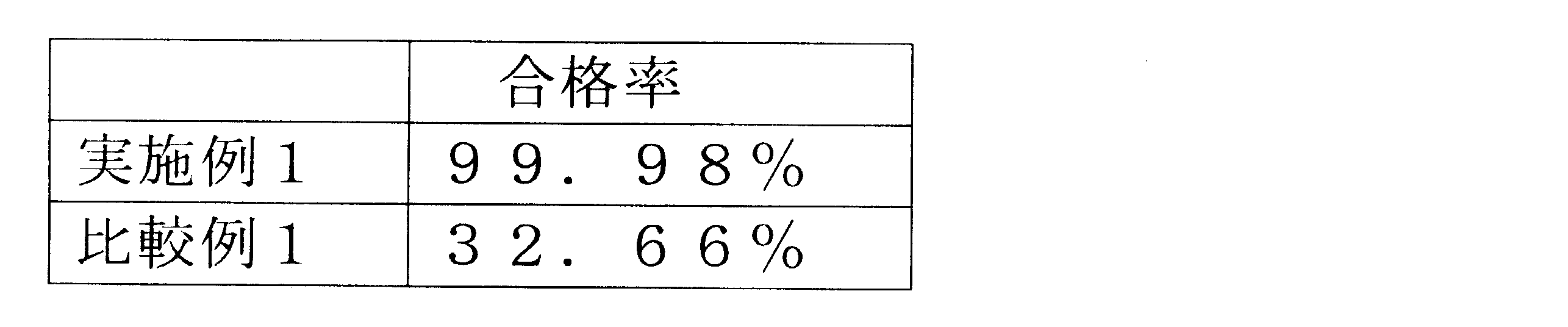
表1の結果から、実施例1では、拭取材を用いて非導電性表面領域を清浄化することにより、ほぼ100%の合格率が得られたが、拭取工程を省略した比較例1では大幅に合格率が低下したことがわかった。このことから、非導電性表面領域を形成する膜除去工程において、光ビームによって除去された第1電極層、光電変換層および第2電極層が導電性付着物として非導電性表面領域に付着しており、この付着物が薄膜太陽電池の絶縁耐電圧性を低下させていること、および、付着物の除去は拭取材による拭き取りが簡単でありながら極めて有効であることが確認できた。
(実施例2)
実施例1の10000個の薄膜太陽電池をアルミフレームまで取り付けて製品化し、それらについても、前記絶縁試験装置を用い、第2電極層4を接地した状態でアルミフレームに6000Vを印可し抵抗値を測定した。そして、実施例2の薄膜太陽電池10000個について、電流値50μm以下の合格率を調べたところ、合格率は99.98%であった。
実施例1の10000個の薄膜太陽電池をアルミフレームまで取り付けて製品化し、それらについても、前記絶縁試験装置を用い、第2電極層4を接地した状態でアルミフレームに6000Vを印可し抵抗値を測定した。そして、実施例2の薄膜太陽電池10000個について、電流値50μm以下の合格率を調べたところ、合格率は99.98%であった。
(実施例3)
図4および図5で説明した実施形態2の構造の薄膜太陽電池を実施例1に準じて1000個作製した。この際、非導電性表面領域8とストリングS2との境界から内側へ1mm離れた位置に、幅200μmの絶縁分離ライン20を形成した。
そして、実施例3の薄膜太陽電池1000個について、実施例1と同様の条件で絶縁試験を行ったところ、合格率は99.90%であった。
図4および図5で説明した実施形態2の構造の薄膜太陽電池を実施例1に準じて1000個作製した。この際、非導電性表面領域8とストリングS2との境界から内側へ1mm離れた位置に、幅200μmの絶縁分離ライン20を形成した。
そして、実施例3の薄膜太陽電池1000個について、実施例1と同様の条件で絶縁試験を行ったところ、合格率は99.90%であった。
(実施例4)
実施例3の1000個の薄膜太陽電池をアルミフレームまで取り付けて製品化し、それらについても、実施例2と同様の条件で絶縁試験を行ったところ、合格率は99.90%であった。
実施例3の1000個の薄膜太陽電池をアルミフレームまで取り付けて製品化し、それらについても、実施例2と同様の条件で絶縁試験を行ったところ、合格率は99.90%であった。
Claims (8)
- 透光性絶縁基板の表面に第1電極層、光電変換層および第2電極層が順次積層されてなる薄膜光電変換素子が複数個互いに電気的に直列接続されたストリングを形成するストリング形成工程と、
前記透光性絶縁基板の表面の外周部に形成されている薄膜光電変換素子部分を光ビームによって除去して非導電性表面領域を全周に形成する膜除去工程と、
前記膜除去工程で発生して前記非導電性表面領域に付着した導電性付着物を除去する清浄化工程とを含むことを特徴とする薄膜太陽電池の製造方法。 - 前記清浄化工程が、拭取材を用いて前記非導電性表面領域に付着した導電性付着物を拭き取ることにより行われる請求項1に記載の薄膜太陽電池の製造方法。
- 前記清浄化工程の後に、清浄化した前記非導電性表面領域の絶縁性を検査する検査工程をさらに含む請求項1に記載の薄膜太陽電池の製造方法。
- 前記検査工程において、前記第2電極層を接地した状態で前記透光性絶縁基板の外周部端面に所定の電圧を印加し、抵抗値が所定値以上であれば合格と判断する請求項3に記載の薄膜太陽電池の製造方法。
- 前記検査工程において、抵抗値が所定値未満である場合、前記清浄化工程および検査工程をこの順に1回以上繰り返す請求項4に記載の薄膜太陽電池の製造方法。
- 前記拭取材が、布、不織布またはスポンジからなる拭取基材に有機溶剤を染み込ませてなる請求項2に記載の薄膜太陽電池の製造方法。
- 請求項1~6のいずれか1つに記載の薄膜太陽電池の製造方法によって製造された薄膜太陽電池であって、
前記透光性絶縁基板の表面に形成された前記ストリングと、透光性絶縁基板の表面の外周部に形成された前記非導電性表面領域とを備え、
非導電性表面領域は、透光性絶縁基板の外周部の端面から平面方向内側へシステム電圧に応じた幅以上の幅で形成されている薄膜太陽電池。 - 前記複数個の薄膜光電変換素子が直列接続する方向と直交する方向に位置する前記非導電性表面領域と前記ストリングとの境界から平面方向内側へ0.5~10mm離れた位置に、薄膜光電変換素子部分が除去されてなる絶縁分離ラインが10~300μmの幅でさらに形成されている請求項7に記載の薄膜太陽電池。
Priority Applications (2)
| Application Number | Priority Date | Filing Date | Title |
|---|---|---|---|
| EP09715527A EP2249395A4 (en) | 2008-02-27 | 2009-02-17 | THIN-LAYER SOLAR BATTERY AND METHOD FOR THE PRODUCTION THEREOF |
| US12/919,139 US20110000521A1 (en) | 2008-02-27 | 2009-02-17 | Thin film solar cell and method for manufacturing the same |
Applications Claiming Priority (2)
| Application Number | Priority Date | Filing Date | Title |
|---|---|---|---|
| JP2008-046640 | 2008-02-27 | ||
| JP2008046640A JP2009206279A (ja) | 2008-02-27 | 2008-02-27 | 薄膜太陽電池およびその製造方法 |
Publications (1)
| Publication Number | Publication Date |
|---|---|
| WO2009107517A1 true WO2009107517A1 (ja) | 2009-09-03 |
Family
ID=41015917
Family Applications (1)
| Application Number | Title | Priority Date | Filing Date |
|---|---|---|---|
| PCT/JP2009/052686 Ceased WO2009107517A1 (ja) | 2008-02-27 | 2009-02-17 | 薄膜太陽電池およびその製造方法 |
Country Status (4)
| Country | Link |
|---|---|
| US (1) | US20110000521A1 (ja) |
| EP (1) | EP2249395A4 (ja) |
| JP (1) | JP2009206279A (ja) |
| WO (1) | WO2009107517A1 (ja) |
Cited By (1)
| Publication number | Priority date | Publication date | Assignee | Title |
|---|---|---|---|---|
| WO2011125651A1 (ja) * | 2010-03-31 | 2011-10-13 | シャープ株式会社 | 太陽電池パネル検査装置、太陽電池パネルの検査方法、太陽電池パネルの製造方法、および太陽電池パネル |
Families Citing this family (106)
| Publication number | Priority date | Publication date | Assignee | Title |
|---|---|---|---|---|
| US6658091B1 (en) | 2002-02-01 | 2003-12-02 | @Security Broadband Corp. | LIfestyle multimedia security system |
| US10237237B2 (en) | 2007-06-12 | 2019-03-19 | Icontrol Networks, Inc. | Communication protocols in integrated systems |
| US11190578B2 (en) | 2008-08-11 | 2021-11-30 | Icontrol Networks, Inc. | Integrated cloud system with lightweight gateway for premises automation |
| US9729342B2 (en) | 2010-12-20 | 2017-08-08 | Icontrol Networks, Inc. | Defining and implementing sensor triggered response rules |
| US12063220B2 (en) | 2004-03-16 | 2024-08-13 | Icontrol Networks, Inc. | Communication protocols in integrated systems |
| US7711796B2 (en) | 2006-06-12 | 2010-05-04 | Icontrol Networks, Inc. | Gateway registry methods and systems |
| US10382452B1 (en) | 2007-06-12 | 2019-08-13 | Icontrol Networks, Inc. | Communication protocols in integrated systems |
| US11582065B2 (en) | 2007-06-12 | 2023-02-14 | Icontrol Networks, Inc. | Systems and methods for device communication |
| US8988221B2 (en) | 2005-03-16 | 2015-03-24 | Icontrol Networks, Inc. | Integrated security system with parallel processing architecture |
| US10721087B2 (en) | 2005-03-16 | 2020-07-21 | Icontrol Networks, Inc. | Method for networked touchscreen with integrated interfaces |
| US11368327B2 (en) | 2008-08-11 | 2022-06-21 | Icontrol Networks, Inc. | Integrated cloud system for premises automation |
| US11677577B2 (en) | 2004-03-16 | 2023-06-13 | Icontrol Networks, Inc. | Premises system management using status signal |
| US11811845B2 (en) | 2004-03-16 | 2023-11-07 | Icontrol Networks, Inc. | Communication protocols over internet protocol (IP) networks |
| US10200504B2 (en) | 2007-06-12 | 2019-02-05 | Icontrol Networks, Inc. | Communication protocols over internet protocol (IP) networks |
| US11159484B2 (en) | 2004-03-16 | 2021-10-26 | Icontrol Networks, Inc. | Forming a security network including integrated security system components and network devices |
| US9141276B2 (en) | 2005-03-16 | 2015-09-22 | Icontrol Networks, Inc. | Integrated interface for mobile device |
| US8635350B2 (en) | 2006-06-12 | 2014-01-21 | Icontrol Networks, Inc. | IP device discovery systems and methods |
| US11113950B2 (en) | 2005-03-16 | 2021-09-07 | Icontrol Networks, Inc. | Gateway integrated with premises security system |
| US10375253B2 (en) | 2008-08-25 | 2019-08-06 | Icontrol Networks, Inc. | Security system with networked touchscreen and gateway |
| US10156959B2 (en) | 2005-03-16 | 2018-12-18 | Icontrol Networks, Inc. | Cross-client sensor user interface in an integrated security network |
| US10313303B2 (en) | 2007-06-12 | 2019-06-04 | Icontrol Networks, Inc. | Forming a security network including integrated security system components and network devices |
| US11368429B2 (en) | 2004-03-16 | 2022-06-21 | Icontrol Networks, Inc. | Premises management configuration and control |
| US11277465B2 (en) | 2004-03-16 | 2022-03-15 | Icontrol Networks, Inc. | Generating risk profile using data of home monitoring and security system |
| US10522026B2 (en) | 2008-08-11 | 2019-12-31 | Icontrol Networks, Inc. | Automation system user interface with three-dimensional display |
| US9531593B2 (en) | 2007-06-12 | 2016-12-27 | Icontrol Networks, Inc. | Takeover processes in security network integrated with premise security system |
| US11244545B2 (en) | 2004-03-16 | 2022-02-08 | Icontrol Networks, Inc. | Cross-client sensor user interface in an integrated security network |
| US10444964B2 (en) | 2007-06-12 | 2019-10-15 | Icontrol Networks, Inc. | Control system user interface |
| US11343380B2 (en) | 2004-03-16 | 2022-05-24 | Icontrol Networks, Inc. | Premises system automation |
| US20090077623A1 (en) | 2005-03-16 | 2009-03-19 | Marc Baum | Security Network Integrating Security System and Network Devices |
| US10142392B2 (en) | 2007-01-24 | 2018-11-27 | Icontrol Networks, Inc. | Methods and systems for improved system performance |
| US10339791B2 (en) | 2007-06-12 | 2019-07-02 | Icontrol Networks, Inc. | Security network integrated with premise security system |
| US11316958B2 (en) | 2008-08-11 | 2022-04-26 | Icontrol Networks, Inc. | Virtual device systems and methods |
| US9191228B2 (en) | 2005-03-16 | 2015-11-17 | Icontrol Networks, Inc. | Cross-client sensor user interface in an integrated security network |
| US11916870B2 (en) | 2004-03-16 | 2024-02-27 | Icontrol Networks, Inc. | Gateway registry methods and systems |
| US20160065414A1 (en) | 2013-06-27 | 2016-03-03 | Ken Sundermeyer | Control system user interface |
| JP2007529826A (ja) | 2004-03-16 | 2007-10-25 | アイコントロール ネットワークス, インコーポレイテッド | 対象事項管理ネットワーク |
| US8963713B2 (en) | 2005-03-16 | 2015-02-24 | Icontrol Networks, Inc. | Integrated security network with security alarm signaling system |
| US11201755B2 (en) | 2004-03-16 | 2021-12-14 | Icontrol Networks, Inc. | Premises system management using status signal |
| US9609003B1 (en) | 2007-06-12 | 2017-03-28 | Icontrol Networks, Inc. | Generating risk profile using data of home monitoring and security system |
| US11489812B2 (en) | 2004-03-16 | 2022-11-01 | Icontrol Networks, Inc. | Forming a security network including integrated security system components and network devices |
| US9306809B2 (en) | 2007-06-12 | 2016-04-05 | Icontrol Networks, Inc. | Security system with networked touchscreen |
| US11496568B2 (en) | 2005-03-16 | 2022-11-08 | Icontrol Networks, Inc. | Security system with networked touchscreen |
| US20120324566A1 (en) | 2005-03-16 | 2012-12-20 | Marc Baum | Takeover Processes In Security Network Integrated With Premise Security System |
| US20170180198A1 (en) | 2008-08-11 | 2017-06-22 | Marc Baum | Forming a security network including integrated security system components |
| US11700142B2 (en) | 2005-03-16 | 2023-07-11 | Icontrol Networks, Inc. | Security network integrating security system and network devices |
| US9450776B2 (en) | 2005-03-16 | 2016-09-20 | Icontrol Networks, Inc. | Forming a security network including integrated security system components |
| US20110128378A1 (en) | 2005-03-16 | 2011-06-02 | Reza Raji | Modular Electronic Display Platform |
| US10999254B2 (en) | 2005-03-16 | 2021-05-04 | Icontrol Networks, Inc. | System for data routing in networks |
| US11615697B2 (en) | 2005-03-16 | 2023-03-28 | Icontrol Networks, Inc. | Premise management systems and methods |
| US12063221B2 (en) | 2006-06-12 | 2024-08-13 | Icontrol Networks, Inc. | Activation of gateway device |
| US10079839B1 (en) | 2007-06-12 | 2018-09-18 | Icontrol Networks, Inc. | Activation of gateway device |
| US11706279B2 (en) | 2007-01-24 | 2023-07-18 | Icontrol Networks, Inc. | Methods and systems for data communication |
| US7633385B2 (en) | 2007-02-28 | 2009-12-15 | Ucontrol, Inc. | Method and system for communicating with and controlling an alarm system from a remote server |
| US8451986B2 (en) | 2007-04-23 | 2013-05-28 | Icontrol Networks, Inc. | Method and system for automatically providing alternate network access for telecommunications |
| US12003387B2 (en) | 2012-06-27 | 2024-06-04 | Comcast Cable Communications, Llc | Control system user interface |
| US10389736B2 (en) | 2007-06-12 | 2019-08-20 | Icontrol Networks, Inc. | Communication protocols in integrated systems |
| US11646907B2 (en) | 2007-06-12 | 2023-05-09 | Icontrol Networks, Inc. | Communication protocols in integrated systems |
| US10523689B2 (en) | 2007-06-12 | 2019-12-31 | Icontrol Networks, Inc. | Communication protocols over internet protocol (IP) networks |
| US11316753B2 (en) | 2007-06-12 | 2022-04-26 | Icontrol Networks, Inc. | Communication protocols in integrated systems |
| US10616075B2 (en) | 2007-06-12 | 2020-04-07 | Icontrol Networks, Inc. | Communication protocols in integrated systems |
| US11601810B2 (en) | 2007-06-12 | 2023-03-07 | Icontrol Networks, Inc. | Communication protocols in integrated systems |
| US11423756B2 (en) | 2007-06-12 | 2022-08-23 | Icontrol Networks, Inc. | Communication protocols in integrated systems |
| US12184443B2 (en) | 2007-06-12 | 2024-12-31 | Icontrol Networks, Inc. | Controlling data routing among networks |
| US11218878B2 (en) | 2007-06-12 | 2022-01-04 | Icontrol Networks, Inc. | Communication protocols in integrated systems |
| US11089122B2 (en) | 2007-06-12 | 2021-08-10 | Icontrol Networks, Inc. | Controlling data routing among networks |
| US10423309B2 (en) | 2007-06-12 | 2019-09-24 | Icontrol Networks, Inc. | Device integration framework |
| US10498830B2 (en) | 2007-06-12 | 2019-12-03 | Icontrol Networks, Inc. | Wi-Fi-to-serial encapsulation in systems |
| US10051078B2 (en) | 2007-06-12 | 2018-08-14 | Icontrol Networks, Inc. | WiFi-to-serial encapsulation in systems |
| US12283172B2 (en) | 2007-06-12 | 2025-04-22 | Icontrol Networks, Inc. | Communication protocols in integrated systems |
| US11212192B2 (en) | 2007-06-12 | 2021-12-28 | Icontrol Networks, Inc. | Communication protocols in integrated systems |
| US10666523B2 (en) | 2007-06-12 | 2020-05-26 | Icontrol Networks, Inc. | Communication protocols in integrated systems |
| US11237714B2 (en) | 2007-06-12 | 2022-02-01 | Control Networks, Inc. | Control system user interface |
| US12541237B2 (en) | 2007-08-10 | 2026-02-03 | Icontrol Networks, Inc. | Integrated security system with parallel processing architecture |
| US10223903B2 (en) | 2010-09-28 | 2019-03-05 | Icontrol Networks, Inc. | Integrated security system with parallel processing architecture |
| US11831462B2 (en) | 2007-08-24 | 2023-11-28 | Icontrol Networks, Inc. | Controlling data routing in premises management systems |
| US11916928B2 (en) | 2008-01-24 | 2024-02-27 | Icontrol Networks, Inc. | Communication protocols over internet protocol (IP) networks |
| US20170185278A1 (en) | 2008-08-11 | 2017-06-29 | Icontrol Networks, Inc. | Automation system user interface |
| US11758026B2 (en) | 2008-08-11 | 2023-09-12 | Icontrol Networks, Inc. | Virtual device systems and methods |
| US11258625B2 (en) | 2008-08-11 | 2022-02-22 | Icontrol Networks, Inc. | Mobile premises automation platform |
| US11729255B2 (en) | 2008-08-11 | 2023-08-15 | Icontrol Networks, Inc. | Integrated cloud system with lightweight gateway for premises automation |
| US11792036B2 (en) | 2008-08-11 | 2023-10-17 | Icontrol Networks, Inc. | Mobile premises automation platform |
| US9628440B2 (en) | 2008-11-12 | 2017-04-18 | Icontrol Networks, Inc. | Takeover processes in security network integrated with premise security system |
| US8638211B2 (en) | 2009-04-30 | 2014-01-28 | Icontrol Networks, Inc. | Configurable controller and interface for home SMA, phone and multimedia |
| AU2011250886A1 (en) | 2010-05-10 | 2013-01-10 | Icontrol Networks, Inc | Control system user interface |
| JP2012023180A (ja) * | 2010-07-14 | 2012-02-02 | Fujifilm Corp | 電子デバイス用基板および該基板を備えた光電変換装置 |
| JP2013219064A (ja) * | 2010-08-05 | 2013-10-24 | Mitsubishi Electric Corp | 光電変換装置の製造方法 |
| US8836467B1 (en) | 2010-09-28 | 2014-09-16 | Icontrol Networks, Inc. | Method, system and apparatus for automated reporting of account and sensor zone information to a central station |
| US11750414B2 (en) | 2010-12-16 | 2023-09-05 | Icontrol Networks, Inc. | Bidirectional security sensor communication for a premises security system |
| US9147337B2 (en) | 2010-12-17 | 2015-09-29 | Icontrol Networks, Inc. | Method and system for logging security event data |
| JP2014099425A (ja) * | 2011-03-07 | 2014-05-29 | Sharp Corp | 薄膜太陽電池の検査装置、薄膜太陽電池の検査方法、薄膜太陽電池の製造方法、および薄膜太陽電池の製造システム |
| DK2720862T3 (en) | 2011-06-17 | 2016-09-19 | Fiberweb Inc | Vapor permeable, water impervious TOTAL MAJOR MULTI-LAYER ARTICLE |
| ES2643697T3 (es) | 2011-06-23 | 2017-11-23 | Fiberweb, Llc | Artículo multicapa permeable al vapor y prácticamente impermeable al agua |
| US10369769B2 (en) | 2011-06-23 | 2019-08-06 | Fiberweb, Inc. | Vapor-permeable, substantially water-impermeable multilayer article |
| WO2012178011A2 (en) | 2011-06-24 | 2012-12-27 | Fiberweb, Inc. | Vapor-permeable, substantially water-impermeable multilayer article |
| US20130186453A1 (en) * | 2011-12-13 | 2013-07-25 | First Solar, Inc | Mitigating photovoltaic module stress damage through cell isolation |
| KR101921237B1 (ko) | 2013-01-16 | 2018-11-22 | 엘지전자 주식회사 | 건물 일체형 태양 전지 모듈 |
| US9928975B1 (en) | 2013-03-14 | 2018-03-27 | Icontrol Networks, Inc. | Three-way switch |
| US9287727B1 (en) | 2013-03-15 | 2016-03-15 | Icontrol Networks, Inc. | Temporal voltage adaptive lithium battery charger |
| US9867143B1 (en) | 2013-03-15 | 2018-01-09 | Icontrol Networks, Inc. | Adaptive Power Modulation |
| EP3031206B1 (en) | 2013-08-09 | 2020-01-22 | ICN Acquisition, LLC | System, method and apparatus for remote monitoring |
| US11405463B2 (en) | 2014-03-03 | 2022-08-02 | Icontrol Networks, Inc. | Media content management |
| US11146637B2 (en) | 2014-03-03 | 2021-10-12 | Icontrol Networks, Inc. | Media content management |
| JP6595866B2 (ja) * | 2015-09-18 | 2019-10-23 | 信越化学工業株式会社 | 太陽光発電システム及びその使用方法 |
| JP2017117870A (ja) * | 2015-12-22 | 2017-06-29 | ソーラーフロンティア株式会社 | 太陽電池モジュール及びその製造方法 |
| CN107123694B (zh) * | 2017-04-20 | 2019-04-30 | 北京四方创能光电科技有限公司 | 一种透光薄膜太阳能电池组件及其制造方法 |
| EP4080588A1 (en) * | 2021-04-23 | 2022-10-26 | Pixquanta Limited | Short-wave infra-red radiation detection device |
Citations (6)
| Publication number | Priority date | Publication date | Assignee | Title |
|---|---|---|---|---|
| JPH10135493A (ja) * | 1996-11-01 | 1998-05-22 | Kanegafuchi Chem Ind Co Ltd | 集積型薄膜光電変換装置 |
| JPH1157631A (ja) * | 1997-08-13 | 1999-03-02 | Fuji Electric Co Ltd | レーザ加工用クリーナ |
| JP2000150944A (ja) * | 1998-11-12 | 2000-05-30 | Kanegafuchi Chem Ind Co Ltd | 太陽電池モジュール |
| JP2000261019A (ja) | 1999-03-10 | 2000-09-22 | Kanegafuchi Chem Ind Co Ltd | 太陽電池モジュール |
| WO2006046397A1 (ja) * | 2004-10-28 | 2006-05-04 | Kaneka Corporation | 薄膜光電変換装置用基板およびそれを用いた集積型薄膜光電変換装置 |
| JP2007035695A (ja) * | 2005-07-22 | 2007-02-08 | Kaneka Corp | 集積型薄膜太陽電池モジュール |
Family Cites Families (9)
| Publication number | Priority date | Publication date | Assignee | Title |
|---|---|---|---|---|
| US7301748B2 (en) * | 1997-04-08 | 2007-11-27 | Anthony Anthony A | Universal energy conditioning interposer with circuit architecture |
| AU731869B2 (en) * | 1998-11-12 | 2001-04-05 | Kaneka Corporation | Solar cell module |
| EP1039554B1 (en) * | 1999-03-25 | 2003-05-14 | Kaneka Corporation | Method of manufacturing thin film solar cell-modules |
| AU772539B2 (en) * | 1999-07-29 | 2004-04-29 | Kaneka Corporation | Method for cleaning photovoltaic module and cleaning apparatus |
| EP1868249B1 (en) * | 1999-09-28 | 2011-07-13 | Kaneka Corporation | Method of controlling manufacturing process of photoelectric conversion apparatus |
| JP4219121B2 (ja) * | 2002-06-21 | 2009-02-04 | 株式会社カネカ | 薄膜光電変換モジュールの製造方法、並びに、製膜装置 |
| JP2004140046A (ja) * | 2002-10-16 | 2004-05-13 | Mitsubishi Heavy Ind Ltd | 薄膜太陽電池 |
| US6888341B2 (en) * | 2003-09-16 | 2005-05-03 | Snap-On Incorporated | Dual voltage circuit tester |
| JP2006332453A (ja) * | 2005-05-27 | 2006-12-07 | Sharp Corp | 薄膜太陽電池の製造方法および薄膜太陽電池 |
-
2008
- 2008-02-27 JP JP2008046640A patent/JP2009206279A/ja active Pending
-
2009
- 2009-02-17 US US12/919,139 patent/US20110000521A1/en not_active Abandoned
- 2009-02-17 WO PCT/JP2009/052686 patent/WO2009107517A1/ja not_active Ceased
- 2009-02-17 EP EP09715527A patent/EP2249395A4/en not_active Withdrawn
Patent Citations (6)
| Publication number | Priority date | Publication date | Assignee | Title |
|---|---|---|---|---|
| JPH10135493A (ja) * | 1996-11-01 | 1998-05-22 | Kanegafuchi Chem Ind Co Ltd | 集積型薄膜光電変換装置 |
| JPH1157631A (ja) * | 1997-08-13 | 1999-03-02 | Fuji Electric Co Ltd | レーザ加工用クリーナ |
| JP2000150944A (ja) * | 1998-11-12 | 2000-05-30 | Kanegafuchi Chem Ind Co Ltd | 太陽電池モジュール |
| JP2000261019A (ja) | 1999-03-10 | 2000-09-22 | Kanegafuchi Chem Ind Co Ltd | 太陽電池モジュール |
| WO2006046397A1 (ja) * | 2004-10-28 | 2006-05-04 | Kaneka Corporation | 薄膜光電変換装置用基板およびそれを用いた集積型薄膜光電変換装置 |
| JP2007035695A (ja) * | 2005-07-22 | 2007-02-08 | Kaneka Corp | 集積型薄膜太陽電池モジュール |
Non-Patent Citations (1)
| Title |
|---|
| See also references of EP2249395A4 |
Cited By (2)
| Publication number | Priority date | Publication date | Assignee | Title |
|---|---|---|---|---|
| WO2011125651A1 (ja) * | 2010-03-31 | 2011-10-13 | シャープ株式会社 | 太陽電池パネル検査装置、太陽電池パネルの検査方法、太陽電池パネルの製造方法、および太陽電池パネル |
| JP2011216645A (ja) * | 2010-03-31 | 2011-10-27 | Sharp Corp | 太陽電池パネル検査装置、太陽電池パネルの検査方法、および太陽電池パネルの製造方法 |
Also Published As
| Publication number | Publication date |
|---|---|
| JP2009206279A (ja) | 2009-09-10 |
| EP2249395A1 (en) | 2010-11-10 |
| EP2249395A4 (en) | 2013-01-16 |
| US20110000521A1 (en) | 2011-01-06 |
Similar Documents
| Publication | Publication Date | Title |
|---|---|---|
| WO2009107517A1 (ja) | 薄膜太陽電池およびその製造方法 | |
| KR101120269B1 (ko) | 광전 변환 장치 및 그 제조 방법 | |
| US20090084433A1 (en) | Thin-film solar battery module and method of producing the same | |
| CN114038922B (zh) | 一种提升绝缘隔离效果的背接触异质结太阳能电池及其制作方法 | |
| US20060112987A1 (en) | Transparent thin-film solar cell module and its manufacturing method | |
| US20100071752A1 (en) | Solar Cell Module Having Buss Adhered With Conductive Adhesive | |
| JP2014017447A (ja) | 集積型薄膜太陽電池およびその製造方法 | |
| WO2008050556A1 (fr) | Cellule solaire à film mince et son procédé de fabrication | |
| WO2010026849A1 (ja) | 集積型薄膜太陽電池 | |
| US11646387B2 (en) | Laser assisted metallization process for solar cell circuit formation | |
| JP3815875B2 (ja) | 集積型薄膜光電変換装置の製造方法 | |
| US6452087B2 (en) | Photovoltaic device and method of fabricating the same | |
| WO2010026850A1 (ja) | 集積型薄膜太陽電池 | |
| US8329495B2 (en) | Method of forming photovoltaic modules | |
| JP2014075470A (ja) | 薄膜太陽電池の製造方法 | |
| JP3520425B2 (ja) | 太陽電池モジュール及びその製造方法 | |
| JP2011181826A (ja) | 光電変換装置の製造方法 | |
| JP2009094272A (ja) | 光電変換モジュールおよび光電変換モジュールの製造方法 | |
| JP2002280580A (ja) | 集積型光起電力装置及びその製造方法 | |
| JP2001127319A (ja) | 太陽電池モジュール及びその製造方法 | |
| WO2014103513A1 (ja) | 太陽電池モジュールおよび太陽電池モジュールの製造方法 | |
| CN204391137U (zh) | 一种非晶硅薄膜太阳能电池 | |
| JP3762013B2 (ja) | 集積型薄膜光電変換装置の製造方法 | |
| US20120024340A1 (en) | Solar Cells With Localized Silicon/Metal Contact For Hot Spot Mitigation and Methods of Manufacture | |
| JP5134075B2 (ja) | 薄膜太陽電池の製造方法 |
Legal Events
| Date | Code | Title | Description |
|---|---|---|---|
| 121 | Ep: the epo has been informed by wipo that ep was designated in this application |
Ref document number: 09715527 Country of ref document: EP Kind code of ref document: A1 |
|
| WWE | Wipo information: entry into national phase |
Ref document number: 12919139 Country of ref document: US |
|
| WWE | Wipo information: entry into national phase |
Ref document number: 2009715527 Country of ref document: EP |
|
| NENP | Non-entry into the national phase |
Ref country code: DE |