WO2009107696A1 - カーボンナノチューブ支持体及びその製造方法 - Google Patents
カーボンナノチューブ支持体及びその製造方法 Download PDFInfo
- Publication number
- WO2009107696A1 WO2009107696A1 PCT/JP2009/053496 JP2009053496W WO2009107696A1 WO 2009107696 A1 WO2009107696 A1 WO 2009107696A1 JP 2009053496 W JP2009053496 W JP 2009053496W WO 2009107696 A1 WO2009107696 A1 WO 2009107696A1
- Authority
- WO
- WIPO (PCT)
- Prior art keywords
- cnt
- support
- carbon
- fixed
- layer
- Prior art date
- Legal status (The legal status is an assumption and is not a legal conclusion. Google has not performed a legal analysis and makes no representation as to the accuracy of the status listed.)
- Ceased
Links
Images









Classifications
-
- G—PHYSICS
- G01—MEASURING; TESTING
- G01Q—SCANNING-PROBE TECHNIQUES OR APPARATUS; APPLICATIONS OF SCANNING-PROBE TECHNIQUES, e.g. SCANNING PROBE MICROSCOPY [SPM]
- G01Q70/00—General aspects of SPM probes, their manufacture or their related instrumentation, insofar as they are not specially adapted to a single SPM technique covered by group G01Q60/00
- G01Q70/08—Probe characteristics
- G01Q70/10—Shape or taper
- G01Q70/12—Nanotube tips
-
- B—PERFORMING OPERATIONS; TRANSPORTING
- B82—NANOTECHNOLOGY
- B82Y—SPECIFIC USES OR APPLICATIONS OF NANOSTRUCTURES; MEASUREMENT OR ANALYSIS OF NANOSTRUCTURES; MANUFACTURE OR TREATMENT OF NANOSTRUCTURES
- B82Y10/00—Nanotechnology for information processing, storage or transmission, e.g. quantum computing or single electron logic
-
- B—PERFORMING OPERATIONS; TRANSPORTING
- B82—NANOTECHNOLOGY
- B82Y—SPECIFIC USES OR APPLICATIONS OF NANOSTRUCTURES; MEASUREMENT OR ANALYSIS OF NANOSTRUCTURES; MANUFACTURE OR TREATMENT OF NANOSTRUCTURES
- B82Y15/00—Nanotechnology for interacting, sensing or actuating, e.g. quantum dots as markers in protein assays or molecular motors
-
- B—PERFORMING OPERATIONS; TRANSPORTING
- B82—NANOTECHNOLOGY
- B82Y—SPECIFIC USES OR APPLICATIONS OF NANOSTRUCTURES; MEASUREMENT OR ANALYSIS OF NANOSTRUCTURES; MANUFACTURE OR TREATMENT OF NANOSTRUCTURES
- B82Y35/00—Methods or apparatus for measurement or analysis of nanostructures
-
- G—PHYSICS
- G01—MEASURING; TESTING
- G01Q—SCANNING-PROBE TECHNIQUES OR APPARATUS; APPLICATIONS OF SCANNING-PROBE TECHNIQUES, e.g. SCANNING PROBE MICROSCOPY [SPM]
- G01Q70/00—General aspects of SPM probes, their manufacture or their related instrumentation, insofar as they are not specially adapted to a single SPM technique covered by group G01Q60/00
- G01Q70/16—Probe manufacture
Definitions
- amorphous carbon when used for fixing CNTs, the low conductivity of amorphous carbon is an important drawback.
- Many nanodevices using CNTs require high conductivity. Examples include a scanning tunneling microscope (STM), which is a kind of SPM, and an electronic circuit using CNTs as nanoelectronic components such as nanotransistors.
- STM scanning tunneling microscope
- amorphous carbon is non-crystalline, and many carbon atoms that form amorphous carbon have an electronic structure of sp 3 , so many electrons are localized and do not contribute to current. Therefore, amorphous carbon has a low conductivity, and is not suitable for the applications requiring the high conductivity described above. In order to improve the performance of the nanodevice described above, it is necessary to make the bonding portion with the CNT highly conductive.
- the amorphous carbon layer is formed at least on the outer surface of the upper graphite layer, the amorphous carbon layer reinforces the graphite layer, and is therefore mechanically strong and conductive.
- the joint part of CNT and support part with high can be obtained.
- the present invention can also be applied to the manufacture of nanodevices such as quantum effect transistors.
- the carbon material layer is formed at the joining position of the support portion, and the CNT is finely formed.
- a nanodevice composed of a CNT circuit board in which an end of the CNT is firmly fixed to the joint part of the circuit board can be manufactured.
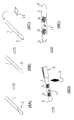
- FIG. 4 is a process diagram for forming a carbon material layer on the knife edge 11. It is a schematic process diagram for explaining a CNT transfer process by a CNT cartridge. It is a TEM photograph which shows the experiment example of fullerene molecular layer formation in a CNT cartridge.
- FIG. 6 is a TEM photograph showing another experimental example in which the mixing concentration and sublimation time are changed from the experiment of FIG. 5. It is a TEM photograph which shows the experimental example which succeeded in thinning of a fullerene molecular layer.
Landscapes
- Chemical & Material Sciences (AREA)
- Engineering & Computer Science (AREA)
- Nanotechnology (AREA)
- Health & Medical Sciences (AREA)
- General Health & Medical Sciences (AREA)
- Physics & Mathematics (AREA)
- General Physics & Mathematics (AREA)
- Nuclear Medicine, Radiotherapy & Molecular Imaging (AREA)
- Radiology & Medical Imaging (AREA)
- Crystallography & Structural Chemistry (AREA)
- Analytical Chemistry (AREA)
- Mathematical Physics (AREA)
- Theoretical Computer Science (AREA)
- Life Sciences & Earth Sciences (AREA)
- Molecular Biology (AREA)
- Carbon And Carbon Compounds (AREA)
Abstract
Description
2 フラーレン溶液
3 フラーレン
4 シリコンカンチレバー材
5 グラスウール材
6 吸引口
7 バーナー
8 真空封印
9 フラーレン分子層
10 堆積物
11 ナイフエッジ
12 電子顕微鏡室
13 カンチレバー
14 突出部
15 CNT
15a 基端部
16 フラーレン分子層
17 電子ビーム
18 支持体
18a 支持部
19 炭素物質層
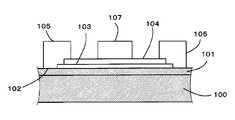
100 シリコン基板
101 酸化膜
102 表面
103 炭素物質層
104 CNT
105 ソース電極層
106 ドレイン電極層
107 ゲート電極層
201 下側グラファイト層
202 上側グラファイト層
203 間隙層
204 補強層
301 電圧グラフ
302 電流グラフ
303 15秒時間帯
304 10秒時間帯
305 10秒時間帯
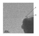
まず、上記形成工程により得られたフラーレン分子層(炭素物質層)の堆積を確認した。図7は、トルエン500μリットルに対して、0.15mMのフラーレンC60の混合濃度のフラーレン溶液を用い、昇華処理を400℃加熱、30分行った実験例のTEM写真を示す。この場合、フラーレン分子層9は約3層の堆積物10からなることがわかる。
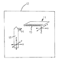
図8はナイフエッジ11への炭素物質層の形成工程を示す。ここで、ナイフエッジ11について説明をする。ナイフエッジ11のエッジ部に複数個のCNT15が配置されたCNTカートリッジが、いずれかのCNTの基端部をカンチレバー13の突出部14に転移させるCNT転移処理に使用される。カンチレバーへのCNT転移工程を簡単に説明する。図9はCNT転移工程を示す。カンチレバー13はカンチレバー部とその先端に形成された突出部14からなるシリコン製部材である。この突出部14にCNT15が対向するようにCNTカートリッジが配置される。カンチレバー13は、3次元移動機構(図示せず)によりXYZの3次元移動が調整でき、また、同様にCNTカートリッジもXYZの3次元移動が可能に配置されている。これらの移動調整により、CNT先端領域(基端部)が突出部14に付着するようにCNT15を転移させる。これらの転移操作は電子顕微鏡室12の中で拡大投影しながら行われる。なお、ナイフエッジ11には、先鋭な刃先を有し、本体表面にCNTを付着可能な構造の基材なら何でもよい。例えば、カミソリ刃やカッターナイフ刃、シリコン片の一辺を先鋭に研磨したもの等が掲げられる。
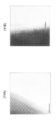
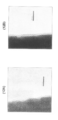
図17は、2つの照射実験例である、電子ビーム照射前と照射後のTEM写真を示す。同図(17A)、(17B)及び(17C)は、それぞれ一照射実験例である、電子ビーム照射前と照射後のTEM写真及びビーム面積(1.0M、5秒)を示す。同図(17D)、(17E)及び(17F)は、別の照射実験例である、電子ビーム照射前と照射後のTEM写真及びビーム面積(1.0M、1秒)を示す。これらの照射実験は前記図11の(11B)のフラーレン溶液による炭素物質層形成条件により得られたフラーレン分子層を用いて行った。同図(17A)、(17B)、(17D)及び(17E)における左側の暗領域は基板であり、これらのTEM写真から、基板上のフラーレン分子層がアモルファス炭素層に変化していることがわかる。
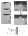
図16はカンチレバー突出部へのCNT固定工程を示す。図16の(16A)は、CNT15をカンチレバー突出部14に転移させた直後を示す。カンチレバー部13及びカンチレバー突出部14の表面にはフラーレン分子層16が上記炭素物質層形工程において膜形成されている。次に、CNT15の基端部15aをカンチレバー突出部14にナイフエッジ11から転移させて、CNT先端部をカンチレバー突出部14から延出させた付着状態において、CNT15の基端部15aに向けて電子ビーム17又はイオンビームを照射する。このビーム照射はTEM内の高真空下で行われる。上記の電子線誘起反応に基づくCNT固定メカニズムにより、高真空(~10-5 Pa)下で観察を行う透過型電子顕微鏡(TEM)内部において、高分解能観察を行いながら、雰囲気中の残留炭化水素が極めて少ない高真空状態下において、前記炭素物質層の分解を行うことにより、強固なCNT固定処理を行うことができる。
Claims (18)
- 支持体の支持部にカーボンナノチューブ(以下、CNTと称する)を固定したCNT支持体において、前記支持部の表面に下側グラファイト層が形成され、前記下側グラファイト層の表面にCNTの固定部が接触して配置され、更に上側グラファイト層が前記固定部を被覆することにより前記CNTが前記支持部に固定されていることを特徴とするCNT支持体。
- 支持体の支持部にCNTを固定したCNT支持体において、前記支持部の表面にCNTの固定部が配置され、前記固定部及びその近傍の前記支持部表面に上側グラファイト層を形成し、前記上側グラファイト層が前記固定部を被覆することにより前記CNTが前記支持部に固定されていることを特徴とするCNT支持体。
- 少なくとも前記上側グラファイト層の外面にアモルファス炭素層が形成された請求項1又は2に記載のCNT支持体。
- 前記支持体がカンチレバーであり、前記支持部が前記カンチレバーに突出形成された突出部であり、前記固定部が前記CNTの基端部であり、前記CNT支持体は、前記突出部に前記CNTの基端部が固定され、前記CNTの先端部が前記突出部から突設されるCNTプローブである請求項1~3のいずれかに記載のCNT支持体。
- 前記支持体が回路基板であり、前記CNTは回路素子であり、前記支持部が前記CNTが接合される接合位置であり、前記固定部が前記CNTの端部であり、前記CNT支持体は、前記接合部に前記CNTの端部が固定されたCNT回路基板である請求項1~3のいずれかに記載のCNT支持体。
- 前記支持体がナイフエッジであり、前記支持部が前記CNTが突出されるエッジ部であり、前記固定部が前記CNTの端部であり、前記CNT支持体は、前記エッジ部に前記CNTの端部が固定されたCNTカートリッジである請求項1~3のいずれかに記載のCNT支持体。
- 前記上側グラファイト層及び/又は前記下側グラファイト層により前記CNTを前記支持部に固定する部位が1箇所以上である請求項1~6のいずれかに記載のCNT支持体。
- 支持体の支持部にCNTを固定したCNT支持体の製造方法において、前記支持部の表面に炭素分子又は有機物からなる炭素物質を堆積した炭素物質層を形成し、前記炭素物質層の表面にCNTの固定部を接触させて配置し、前記固定部及び/又は固定部近傍の被照射領域に電子ビーム又はイオンビームを照射して前記炭素物質層を分解し、前記分解により形成された炭素膜により前記固定部を被覆して前記CNTを前記支持部に固定することを特徴とするCNT支持体の製造方法。
- 支持体の支持部にCNTを固定したCNT支持体の製造方法において、前記支持部の表面にCNTの固定部を配置し、前記固定部及び/又はその近傍の前記支持部表面に炭素分子又は有機物からなる炭素物質を堆積した炭素物質層を形成し、前記固定部及び/又は固定部近傍の被照射領域に電子ビーム又はイオンビームを照射して前記炭素物質層を分解し、前記分解により形成された炭素膜により前記固定部を被覆して前記CNTを前記支持部に固定することを特徴とするCNT支持体の製造方法。
- 所定質量の前記炭素物質を容器内に配置し、前記容器内に前記支持体を投入して前記容器を封止し、前記容器を加熱して前記炭素物質を蒸発させて前記炭素物質を前記支持部を含む前記支持体の表面に堆積させて前記炭素物質層を形成する請求項8又は9に記載のCNT支持体の製造方法。
- 前記炭素物質を溶媒に混合した所定濃度の炭素物質溶液を調製し、前記炭素物質溶液の所定容量を前記容器中に注入し、加熱により前記容器から溶媒を除去して前記所定質量の炭素物質を前記容器内に残留配置させる請求項10に記載のCNT支持体の製造方法。
- 前記炭素膜により前記CNTの前記固定部を前記支持部に被覆固定した後、前記CNT支持体を洗浄溶媒により洗浄するか、又は前記支持体を加熱して、前記CNT支持体の表面に付着している前記炭素物質を除去する請求項10又は11に記載のCNT支持体の製造方法。
- 前記炭素膜が、アモルファス炭素膜、又はグラファイト膜である請求項8~11のいずれかに記載のCNT支持体の製造方法。
- 前記炭素分子が、フラーレン又は金属内包フラーレンである請求項8~13のいずれかに記載のCNT支持体の製造方法。
- 前記有機物は炭素以外の成分を含有し、前記分解により前記炭素以外の成分が気散して前記炭素膜が形成される請求項8~13のいずれかに記載のCNT支持体の製造方法。
- 前記支持体がカンチレバーであり、前記支持部が前記カンチレバーに突出形成された突出部であり、前記固定部が前記CNTの基端部であり、前記CNT支持体は、前記突出部に前記CNTの基端部が固定され、前記CNTの先端部が前記突出部から突設されるCNTプローブである請求項8~15のいずれかに記載のCNT支持体の製造方法。
- 前記支持体が回路基板であり、前記CNTは回路素子であり、前記支持部が前記CNTが接合される接合位置であり、前記固定部が前記CNTの端部であり、前記CNT支持体は、前記接合部に前記CNTの端部が固定されたCNT回路基板である請求項8~15のいずれかに記載のCNT支持体の製造方法。
- 前記支持体がナイフエッジであり、前記支持部が前記CNTが突出されるエッジ部であり、前記固定部が前記CNTの端部であり、前記CNT支持体は、前記エッジ部に前記CNTの端部が固定されたCNTカートリッジである請求項8~15のいずれかに記載のCNT支持体の製造方法。
Priority Applications (4)
| Application Number | Priority Date | Filing Date | Title |
|---|---|---|---|
| US12/735,969 US20110000703A1 (en) | 2008-02-27 | 2009-02-26 | Carbon nanotube supporting body and process for producing the carbon nanotube supporting body |
| EP09714780A EP2259043A4 (en) | 2008-02-27 | 2009-02-26 | CARBON FAN TUBE CARRIER AND METHOD FOR PRODUCING THE CARBON FAN TUBE CARRIER |
| CN2009801069105A CN101960286A (zh) | 2008-02-27 | 2009-02-26 | 碳纳米管支持体及其制造方法 |
| JP2010500728A JP4917170B2 (ja) | 2008-02-27 | 2009-02-26 | カーボンナノチューブ支持体及びその製造方法 |
Applications Claiming Priority (2)
| Application Number | Priority Date | Filing Date | Title |
|---|---|---|---|
| JP2008045920 | 2008-02-27 | ||
| JP2008-045920 | 2008-02-27 |
Publications (1)
| Publication Number | Publication Date |
|---|---|
| WO2009107696A1 true WO2009107696A1 (ja) | 2009-09-03 |
Family
ID=41016084
Family Applications (1)
| Application Number | Title | Priority Date | Filing Date |
|---|---|---|---|
| PCT/JP2009/053496 Ceased WO2009107696A1 (ja) | 2008-02-27 | 2009-02-26 | カーボンナノチューブ支持体及びその製造方法 |
Country Status (6)
| Country | Link |
|---|---|
| US (1) | US20110000703A1 (ja) |
| EP (1) | EP2259043A4 (ja) |
| JP (1) | JP4917170B2 (ja) |
| KR (1) | KR20100098451A (ja) |
| CN (1) | CN101960286A (ja) |
| WO (1) | WO2009107696A1 (ja) |
Cited By (3)
| Publication number | Priority date | Publication date | Assignee | Title |
|---|---|---|---|---|
| WO2014017340A1 (ja) | 2012-07-25 | 2014-01-30 | 東レ株式会社 | プリプレグおよび炭素繊維強化複合材料 |
| JP2014510003A (ja) * | 2010-12-31 | 2014-04-24 | ▲海▼洋王照明科技股▲ふん▼有限公司 | 炭素被覆酸化グラフェン複合材料並びにその製造方法及びその応用 |
| JP2018067581A (ja) * | 2016-10-17 | 2018-04-26 | 富士通株式会社 | カーボンナノチューブ構造、放熱シート及びカーボンナノチューブ構造の製造方法 |
Families Citing this family (4)
| Publication number | Priority date | Publication date | Assignee | Title |
|---|---|---|---|---|
| US8564027B2 (en) | 2012-01-27 | 2013-10-22 | International Business Machines Corporation | Nano-devices formed with suspended graphene membrane |
| KR20140115836A (ko) * | 2013-03-22 | 2014-10-01 | 삼성전자주식회사 | 햅틱 효과를 제공하는 휴대 단말 및 방법 |
| KR101958323B1 (ko) * | 2016-11-22 | 2019-03-15 | 주식회사 하이딥 | 압력 감지부 및 이를 포함하는 터치 입력 장치 |
| CN109909493A (zh) * | 2019-02-25 | 2019-06-21 | 华中科技大学 | 一种电子束辐照提高金属材料稳定性的方法 |
Citations (5)
| Publication number | Priority date | Publication date | Assignee | Title |
|---|---|---|---|---|
| JPH10261712A (ja) * | 1997-03-19 | 1998-09-29 | Sanyo Electric Co Ltd | 導電領域の形成方法及び薄膜素子 |
| JP2000227435A (ja) | 1998-12-03 | 2000-08-15 | Yoshikazu Nakayama | 電子装置の表面信号操作用プローブ及びその製造方法 |
| JP2000249712A (ja) | 1998-12-31 | 2000-09-14 | Yoshikazu Nakayama | 電子装置の表面信号操作用融着プローブ及びその製造方法 |
| JP2002162336A (ja) * | 2000-11-26 | 2002-06-07 | Yoshikazu Nakayama | 導電性走査型顕微鏡用プローブ及びこれを用いた加工方法 |
| JP2007232668A (ja) * | 2006-03-03 | 2007-09-13 | Nagoya Institute Of Technology | カーボン細線プローブ |
Family Cites Families (8)
| Publication number | Priority date | Publication date | Assignee | Title |
|---|---|---|---|---|
| DE69935422T2 (de) * | 1998-12-03 | 2007-11-29 | Daiken Chemical Co. Ltd. | Oberflächen-signal-kommando-sonde eines elektronischen gerätes und verfahren zu ihrer herstellung |
| JP3863721B2 (ja) * | 2000-12-07 | 2006-12-27 | 喜萬 中山 | ナノチューブカートリッジの製造方法 |
| JP4997674B2 (ja) * | 2001-09-03 | 2012-08-08 | 日本電気株式会社 | 二次電池用負極および二次電池 |
| KR100837393B1 (ko) * | 2002-01-22 | 2008-06-12 | 삼성에스디아이 주식회사 | 탄소와 친화도가 높은 금속을 전극으로 구비하는 전자소자 |
| JP4180289B2 (ja) * | 2002-03-18 | 2008-11-12 | 喜萬 中山 | ナノチューブ先鋭化方法 |
| JP3832402B2 (ja) * | 2002-08-12 | 2006-10-11 | 株式会社日立製作所 | カーボンナノチューブを有する電子源とそれを用いた電子顕微鏡および電子線描画装置 |
| JP2005083857A (ja) * | 2003-09-08 | 2005-03-31 | Yoshikazu Nakayama | ナノチューブプローブ及び製造方法 |
| JP5102968B2 (ja) * | 2006-04-14 | 2012-12-19 | 株式会社日立ハイテクノロジーズ | 導電性針およびその製造方法 |
-
2009
- 2009-02-26 WO PCT/JP2009/053496 patent/WO2009107696A1/ja not_active Ceased
- 2009-02-26 US US12/735,969 patent/US20110000703A1/en not_active Abandoned
- 2009-02-26 CN CN2009801069105A patent/CN101960286A/zh active Pending
- 2009-02-26 EP EP09714780A patent/EP2259043A4/en not_active Withdrawn
- 2009-02-26 JP JP2010500728A patent/JP4917170B2/ja not_active Expired - Fee Related
- 2009-02-26 KR KR1020107016448A patent/KR20100098451A/ko not_active Abandoned
Patent Citations (5)
| Publication number | Priority date | Publication date | Assignee | Title |
|---|---|---|---|---|
| JPH10261712A (ja) * | 1997-03-19 | 1998-09-29 | Sanyo Electric Co Ltd | 導電領域の形成方法及び薄膜素子 |
| JP2000227435A (ja) | 1998-12-03 | 2000-08-15 | Yoshikazu Nakayama | 電子装置の表面信号操作用プローブ及びその製造方法 |
| JP2000249712A (ja) | 1998-12-31 | 2000-09-14 | Yoshikazu Nakayama | 電子装置の表面信号操作用融着プローブ及びその製造方法 |
| JP2002162336A (ja) * | 2000-11-26 | 2002-06-07 | Yoshikazu Nakayama | 導電性走査型顕微鏡用プローブ及びこれを用いた加工方法 |
| JP2007232668A (ja) * | 2006-03-03 | 2007-09-13 | Nagoya Institute Of Technology | カーボン細線プローブ |
Non-Patent Citations (4)
| Title |
|---|
| H. DAI ET AL., NATURE, vol. 384, 14 November 1996 (1996-11-14), pages 147 - 150 |
| H.DAI, NATURE, vol. 384, 14 November 1996 (1996-11-14), pages 147 - 150 |
| HISANORI SHINOHARA; YAHACHI SAITO: "Chemistry and Physics of Fullerene", January 1997, NAGOYA UNIVERSITY PUBLICATION SOCIETY |
| See also references of EP2259043A4 * |
Cited By (6)
| Publication number | Priority date | Publication date | Assignee | Title |
|---|---|---|---|---|
| JP2014510003A (ja) * | 2010-12-31 | 2014-04-24 | ▲海▼洋王照明科技股▲ふん▼有限公司 | 炭素被覆酸化グラフェン複合材料並びにその製造方法及びその応用 |
| WO2014017340A1 (ja) | 2012-07-25 | 2014-01-30 | 東レ株式会社 | プリプレグおよび炭素繊維強化複合材料 |
| US9765194B2 (en) | 2012-07-25 | 2017-09-19 | Toray Industries, Inc. | Prepreg and carbon fiber-reinforced composite material |
| US11111345B2 (en) | 2012-07-25 | 2021-09-07 | Toray Industries, Inc. | Prepreg and carbon fiber-reinforced composite material |
| US11286359B2 (en) | 2012-07-25 | 2022-03-29 | Toray Industries, Inc. | Prepreg and carbon fiber-reinforced composite material |
| JP2018067581A (ja) * | 2016-10-17 | 2018-04-26 | 富士通株式会社 | カーボンナノチューブ構造、放熱シート及びカーボンナノチューブ構造の製造方法 |
Also Published As
| Publication number | Publication date |
|---|---|
| EP2259043A1 (en) | 2010-12-08 |
| CN101960286A (zh) | 2011-01-26 |
| JP4917170B2 (ja) | 2012-04-18 |
| US20110000703A1 (en) | 2011-01-06 |
| KR20100098451A (ko) | 2010-09-06 |
| EP2259043A4 (en) | 2012-06-27 |
| JPWO2009107696A1 (ja) | 2011-07-07 |
Similar Documents
| Publication | Publication Date | Title |
|---|---|---|
| JP4917170B2 (ja) | カーボンナノチューブ支持体及びその製造方法 | |
| US7076871B2 (en) | Method of manufacturing a carbon nanotube device | |
| JPWO2006025393A1 (ja) | ナノスケールの低次元量子構造体の製造方法、及び、当該製造方法を用いた集積回路の製造方法 | |
| Zhou et al. | Laser-assisted nanofabrication of carbon nanostructures | |
| Snowdon | Methods of the Alignment-Relay Technique for Nanosystems: Optimization and Innovation | |
| JP2007070155A (ja) | 内包体、内包体の製造方法および製造装置 | |
| Lee et al. | Characterization of plasma synthesized vertical carbon nanofibers for nanoelectronics applications | |
| Rousseau et al. | Elaboration and Magnetic Properties of Cobalt-Palladium Magnetic Nanowires Encapsulated in Carbon Nanotubes | |
| Narayana | A study of electronic structure and thermal stability of engineered SOI material | |
| Freitag | Local electronic functionality in carbon nanotube devices | |
| Radosavljevic | Improving carbon nanotube nanodevices: Ambipolar field effect transistors and high-current interconnects | |
| Mahjouri et al. | Growth of self-aligned single-walled carbon nanotubes by laser-assisted chemical vapor deposition | |
| Durkop | Electronic properties of carbon nanotubes studied in field-effect transistor geometries | |
| Jin | Synthesis, characterization and manipulation of Carbon nanotubes | |
| Frielinghaus | Structural influences on electrical transport in nanostructures | |
| Schaefer | Carbon Nanostructures–Tubes, Graphene, Fullerenes, Wave-Particle Duality | |
| de Asis Jr et al. | Carbon nanotube atomic force microscopy with applications to biology and electronics | |
| Gnisci | Ethanol-CVD growth of large single-crystal graphene and graphene-based derivative for photovoltaic applications | |
| Fujita | Surface Nanocharacterization of Fullerene Nanowhiskers | |
| Hofmann et al. | Direct synthesis and integration of SWNT devices | |
| Ghosh | CNT field emission cell with built-in electron beam source for electron stimulated amplified field emission | |
| Papadopoulos | Nanotube engineering and science, synthesis and properties of highly ordered carbon nanotube arrays and Y-junction carbon nanotubes | |
| Yi | Ballistic conduction in multiwalled carbon nanotubes at room temperature | |
| Clausen | Transmission Electron Microscopy Study of Individual Carbon Nanotube Breakdown Caused by Joule Heating in Air | |
| Siriwardena | Scanning Tunneling Microscopy Study of the Dynamic Movement of Confined Molecules in Self-Assembled Molecular Fences |
Legal Events
| Date | Code | Title | Description |
|---|---|---|---|
| WWE | Wipo information: entry into national phase |
Ref document number: 200980106910.5 Country of ref document: CN |
|
| 121 | Ep: the epo has been informed by wipo that ep was designated in this application |
Ref document number: 09714780 Country of ref document: EP Kind code of ref document: A1 |
|
| ENP | Entry into the national phase |
Ref document number: 20107016448 Country of ref document: KR Kind code of ref document: A |
|
| WWE | Wipo information: entry into national phase |
Ref document number: 2010500728 Country of ref document: JP |
|
| WWE | Wipo information: entry into national phase |
Ref document number: 12735969 Country of ref document: US |
|
| NENP | Non-entry into the national phase |
Ref country code: DE |
|
| WWE | Wipo information: entry into national phase |
Ref document number: 2009714780 Country of ref document: EP |