WO2009119773A1 - 発光装置 - Google Patents
発光装置 Download PDFInfo
- Publication number
- WO2009119773A1 WO2009119773A1 PCT/JP2009/056195 JP2009056195W WO2009119773A1 WO 2009119773 A1 WO2009119773 A1 WO 2009119773A1 JP 2009056195 W JP2009056195 W JP 2009056195W WO 2009119773 A1 WO2009119773 A1 WO 2009119773A1
- Authority
- WO
- WIPO (PCT)
- Prior art keywords
- light emitting
- emitting element
- voltage
- light
- circuit
- Prior art date
- Legal status (The legal status is an assumption and is not a legal conclusion. Google has not performed a legal analysis and makes no representation as to the accuracy of the status listed.)
- Ceased
Links
Images



Classifications
-
- H—ELECTRICITY
- H05—ELECTRIC TECHNIQUES NOT OTHERWISE PROVIDED FOR
- H05B—ELECTRIC HEATING; ELECTRIC LIGHT SOURCES NOT OTHERWISE PROVIDED FOR; CIRCUIT ARRANGEMENTS FOR ELECTRIC LIGHT SOURCES, IN GENERAL
- H05B45/00—Circuit arrangements for operating light-emitting diodes [LED]
- H05B45/60—Circuit arrangements for operating LEDs comprising organic material, e.g. for operating organic light-emitting diodes [OLED] or polymer light-emitting diodes [PLED]
-
- H—ELECTRICITY
- H10—SEMICONDUCTOR DEVICES; ELECTRIC SOLID-STATE DEVICES NOT OTHERWISE PROVIDED FOR
- H10K—ORGANIC ELECTRIC SOLID-STATE DEVICES
- H10K50/00—Organic light-emitting devices
- H10K50/10—OLEDs or polymer light-emitting diodes [PLED]
-
- H—ELECTRICITY
- H10—SEMICONDUCTOR DEVICES; ELECTRIC SOLID-STATE DEVICES NOT OTHERWISE PROVIDED FOR
- H10K—ORGANIC ELECTRIC SOLID-STATE DEVICES
- H10K50/00—Organic light-emitting devices
-
- H—ELECTRICITY
- H10—SEMICONDUCTOR DEVICES; ELECTRIC SOLID-STATE DEVICES NOT OTHERWISE PROVIDED FOR
- H10K—ORGANIC ELECTRIC SOLID-STATE DEVICES
- H10K71/00—Manufacture or treatment specially adapted for the organic devices covered by this subclass
- H10K71/861—Repairing
-
- Y—GENERAL TAGGING OF NEW TECHNOLOGICAL DEVELOPMENTS; GENERAL TAGGING OF CROSS-SECTIONAL TECHNOLOGIES SPANNING OVER SEVERAL SECTIONS OF THE IPC; TECHNICAL SUBJECTS COVERED BY FORMER USPC CROSS-REFERENCE ART COLLECTIONS [XRACs] AND DIGESTS
- Y02—TECHNOLOGIES OR APPLICATIONS FOR MITIGATION OR ADAPTATION AGAINST CLIMATE CHANGE
- Y02B—CLIMATE CHANGE MITIGATION TECHNOLOGIES RELATED TO BUILDINGS, e.g. HOUSING, HOUSE APPLIANCES OR RELATED END-USER APPLICATIONS
- Y02B20/00—Energy efficient lighting technologies, e.g. halogen lamps or gas discharge lamps
- Y02B20/30—Semiconductor lamps, e.g. solid state lamps [SSL] light emitting diodes [LED] or organic LED [OLED]
Definitions
- the present invention relates to a light emitting device, and in particular, can apply a reverse voltage to a light emitting element that is abnormal and flow a refresh current to restore the light emitting element that is abnormal, and stress the normal light emitting element.
- the present invention relates to a light-emitting device that can be avoided.
- An organic electroluminescent device is a light emitting device that utilizes a phenomenon in which light is emitted by excitons generated by recombination of electrons and holes injected into an organic substance.
- a display using this organic electroluminescent device has been actively developed. This is because the organic electroluminescent device has a wide viewing angle, a fast response speed, a high contrast, and the like as compared with the liquid crystal display device.
- an organic electroluminescent device has a structure in which an organic layer is sandwiched between a cathode and an anode. When a voltage is applied, electrons are injected as carriers from the cathode and holes are injected from the anode, respectively. When these carriers recombine inside the organic layer, excitons are generated to emit light.
- the organic electroluminescent device generally includes an organic layer including a light emitting layer, a hole transport layer, an electron transport layer, and the like, and a pair of electrodes (cathode and anode) disposed so as to face each other through the organic layer. ).
- the organic layer has a very thin layer thickness of, for example, about 100 nm. Therefore, there is a risk that leakage defects may occur between the electrodes, or insulation withstand voltage defects between the electrodes may occur due to the mixing of minute foreign substances or uneven formation of the organic layer.
- the insulation failure portion is insulated, so that the emission colors are mutually different. Repair of defective insulation between a pair of electrodes of an organic electroluminescent device comprising a plurality of types of organic layers including at least different light emitting layers and a pair of electrodes arranged opposite to each other via the plurality of types of organic layers There is a known method (see, for example, Patent Document 1).
- the cathode includes the first conductive layer and the buffer.
- a method for manufacturing an organic electroluminescent element in which a layer and a second conductive layer are sequentially arranged, and aging is performed after forming a laminate.
- a first conductive layer, a buffer layer, and a second conductive layer are sequentially laminated to form a cathode, and after the laminate is formed, aging is performed, whereby an organic electroluminescent device having a lower driving voltage than conventional ones.
- a nescent element can be manufactured (see, for example, Patent Document 2).
- a DC power supply means for supplying a desired DC voltage to the organic electroluminescent element a detection means for detecting the stop of the voltage supply of the DC power supply means, and the organic electroluminescence when the voltage supply of the DC power supply means is stopped.
- an illumination device including reverse voltage supply means for supplying a reverse characteristic voltage to the luminescent element (Patent Document 3). JP 2007-207703 JP 2007-200662 JP 2007-149463 A
- Patent Document 1 As described above, in the method for repairing an organic electroluminescent element disclosed in Patent Document 1, when the organic electroluminescent element exhibits an abnormal voltage, a reverse voltage is applied by operating a forward / reverse inverting circuit for refreshing. However, since no current flows through the normal organic electroluminescent element, it is necessary to turn off the normal organic electroluminescent element and provide a time for refreshing individually. On the other hand, in Patent Document 3, when the stop of the voltage supply of the DC power supply means is detected, a voltage having a reverse characteristic is supplied to the organic electroluminescent element. It is necessary to provide time. Further, not only can a light be applied to an electroluminescent element that does not require refreshing, but it is not lighted, but also stress is applied.
- a forward / reverse inversion circuit is operated for refreshing.
- a reverse voltage When a reverse voltage is applied, no current flows through a normal light emitting element, and thus the light emitting element cannot be refreshed.
- the present invention has been made in view of the above circumstances, and can apply a reverse voltage to a light emitting element that is abnormal and flow a refresh current to recover the light emitting element that is abnormal and normal.
- An object of the present invention is to provide a light emitting device that can avoid applying stress to the light emitting element.
- the present invention is a light emitting device having one or a plurality of light emitting elements that emit light when supplied with a direct current, and a direct current power supply circuit that supplies a predetermined current or more to the light emitting elements, and is applied to the light emitting elements.
- a light emitting element voltage detection circuit that detects a voltage to be detected, and a forward / reverse inversion circuit that applies a reverse voltage to the light emitting element that has detected the abnormality when the light emitting element voltage detection circuit detects the abnormality of the light emitting element. It is characterized by being.
- the forward / reverse inverting circuit assigned to the light emitting element is provided and the light emitting element voltage detecting circuit for detecting the voltage applied to the light emitting element is provided, an abnormal light emitting element can be detected.
- the forward / reverse inverting circuit includes a shorting switch that short-circuits a normal light emitting element when a reverse voltage is applied to the light emitting element in which an abnormality is detected.
- the forward / reverse inverting circuit assigned to the light emitting element and the short circuit switch provided for each light emitting element are provided, the reverse voltage is surely applied to the abnormal light emitting element, while the normal light emitting element is provided. Therefore, it is possible to avoid applying a reverse voltage, to recover the abnormal light emitting element, and to avoid stressing the normal light emitting element.
- the plurality of light-emitting elements are connected in series, the short-circuit switch is connected in parallel to each of the plurality of light-emitting elements, and the light-emitting element voltage detection circuit includes the plurality of light-emitting elements. A voltage applied to each light emitting element is detected, and abnormality of the light emitting element is detected by a change in voltage value.
- the short-circuit switch is a field effect transistor.
- the short-circuit switch is a thyristor.
- the thyristor when a reverse voltage is applied to the light emitting element, the thyristor is automatically turned on to protect the light emitting element, so that a drive IC for driving the thyristor becomes unnecessary, and the configuration of the light emitting device is simplified.
- the light-emitting device of the present invention is characterized in that the forward / reverse inversion circuit includes a light-emitting element current detection circuit that detects a current flowing through the light-emitting element.
- the forward / reverse inverting circuit is connected in series between power supplies, and the first and second switching elements whose series connection points are connected to one end of the one or more light emitting elements
- the power supply includes a third and a fourth switching element connected in series between the power supplies, the series connection point being connected to the other end of the one or more light emitting elements, and the second and third switching elements are A reverse voltage is applied to the light emitting element that is detected to be abnormal by conduction and refreshed, and a forward voltage is applied to the light emitting element that is refreshed by conducting the first and fourth switching elements.
- the light emitting element can be refreshed by applying a reverse voltage to the light emitting element, and the abnormal light emitting element can be restored, leading to an improvement in the life of the light emitting element.
- the light emitting element voltage detection circuit detects that an abnormal light emitting element has returned to normal due to a voltage change of the light emitting element or elements, and the forward / reverse inversion circuit is normal. A forward voltage is applied to the light-emitting element that has returned to the above.
- the light emitting element when an abnormal light emitting element returns to normal, the light emitting element can be made to emit light again, so that the life of the light emitting element can be extended. Moreover, since it can detect only with the change of the voltage value which generate
- the light-emitting element current detection circuit detects that an abnormal light-emitting element has returned to normal due to a current change in the one or more light-emitting elements, and the forward / reverse inversion circuit is normal A forward voltage is applied to the light-emitting element that has returned to the above.
- the light emitting element when an abnormal light emitting element returns to normal, the light emitting element can be made to emit light again, so that the life of the light emitting element can be extended. Moreover, since it can detect only with the change of the electric current value which generate
- the lighting fixture of the present invention is constituted by the above light emitting device including a plurality of light emitting elements composed of one or a plurality of organic electroluminescent elements.
- the forward / reverse inverting circuit assigned to the light emitting element is provided and the light emitting element voltage detecting circuit for detecting the voltage applied to the light emitting element is provided.
- An abnormal element can be detected, a reverse voltage can be reliably applied to the abnormal light emitting element, a refresh current can be applied to recover the abnormal light emitting element, and stress can be applied to the normal light emitting element. You can avoid that.
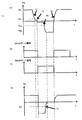
- 1 is a time chart showing a flow of operations of the light-emitting device 100 according to the first embodiment of the present invention.
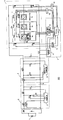
- FIG. 1 is a diagram for explaining a configuration of a light emitting device 100 according to an embodiment of the present invention.
- the light emitting device 100 according to the present embodiment includes a power factor correction circuit 2 (hereinafter referred to as a PFC (Power Factor Correction) circuit 2) to which DC power is supplied from a diode bridge DB that rectifies an AC power source 1, and a PFC circuit 2.
- a PFC Power Factor Correction
- the step-down chopper circuit 4 that converts the output voltage of the output to the light-emitting element
- the forward / reverse inversion circuit 6 that switches the current supplied to the light-emitting element 8
- the light-emitting element current detection circuit 11 the light-emitting element voltage detection circuit 12, and the drive IC 13 , 14 and a microcomputer 16
- a light emitting element voltage / current control circuit 7 for controlling the voltage and current of the light emitting element 8.
- the forward / reverse inverting circuit 6 assigned to the light emitting element 8 is provided, the reverse current is surely applied to the light emitting element 8 which has become abnormal to refresh the current.
- the light emitting element 8 that has become abnormal can be recovered.
- the light emitting element voltage detection circuit 12 detects abnormality of the light emitting element 8 only by the change of the voltage value which generate
- Embodiment 1 of the present invention will be described with reference to FIG.
- Vla is a voltage applied to the light emitting element 8
- Ila is a current flowing through the light emitting element 8.
- the light-emitting element 8 in the first embodiment is an organic electroluminescent panel and has an anode and a cathode. When flowing from the anode to the cathode, the organic electroluminescent panel emits light.
- the PFC circuit 2 is a circuit that converts an AC voltage into a DC voltage.
- the switching element Q1 of the PFC circuit 2 operates at several tens kHz to several hundreds kHz. Note that a circuit system that is a DC power supply or a DC power supply may be used instead of the PFC circuit 2.
- the step-down chopper circuit 4 is a circuit that converts a DC voltage into a DC voltage.
- the switching element Q2 of the step-down chopper circuit 4 operates at several tens kHz to several hundreds kHz. Note that a circuit system that is a direct current power supply or a direct current power supply may be used instead of the step-down chopper circuit 4.
- the main operation flow is as follows: (1) An abnormality of the light emitting element 8 is detected. (2) A voltage in the opposite direction to normal is applied to the light emitting element 8. (3) Detecting that the light emitting element 8 has returned to normal. (4) A normal current is passed through the light emitting element 8.
- FIG. 2 shows a time chart of the operation flow.
- T1 An abnormality of the light emitting element 8 is detected.
- Vla voltage applied to the light emitting element
- the light emitting element voltage detection circuit 12 detects that Vla has dropped, and sends a signal to the microcomputer 16.
- a reverse voltage is applied to the light emitting element 8 (T2).
- Vla decreases to Vth1
- the microcomputer 16 sends a signal to the drive ICs 1, 2 (13, 14), turns off the switching elements Q3, Q6 and turns on the switching elements Q4, Q5. Therefore, a reverse voltage is applied to the light emitting element 8. At this time, a reverse current (refresh current) flows through the light emitting element 8.
- a normal current is passed through the light emitting element 8 (T4).
- Vla drops to Vth2 (Ila becomes Ith1 or more)
- the microcomputer 16 sends a signal to the drive ICs 1, 2 (13, 14), turns on the switching elements Q3, Q6 and turns off the switching elements Q4, Q5. . Therefore, a current flows through the light emitting element 8 in the same direction as normal, and the light emitting element 8 emits light.
- the forward / reverse inverting circuit 6 assigned to the light emitting element 8 is provided, the reverse current is surely applied to the light emitting element 8 which has become abnormal to refresh the current.
- the light emitting element 8 that has become abnormal can be recovered.
- the light emitting element 8 when the abnormal light emitting element 8 returns to normal, the light emitting element 8 can emit light again, so that the life of the light emitting element 8 can be extended. Furthermore, since the light-emitting element voltage detection circuit 12 or the light-emitting element current detection circuit 11 can detect normal return of the light-emitting element 8 only by a change in voltage value or current value generated in the light-emitting element 8, the number of parts and the control target are reduced. can do.
- FIG. 3 is a diagram for explaining the configuration of the light emitting device 100 according to the second embodiment of the present invention.
- Vla is a voltage applied to the entire light emitting elements 8a, 8b and 8c
- Vla1 is a voltage applied to the light emitting element 8a
- Vla2 is a voltage applied to the light emitting element 8b
- Vla3 is applied to the light emitting element 8c.
- Voltage. Ila is a current flowing through the light emitting elements 8a, 8b, and 8c.
- the light emitting elements 8a, 8b, 8c are organic electroluminescent panels, and each light emitting element 8a, 8b, 8c has a pair of an anode and a cathode.
- the PFC circuit 2 is the same as that of the first embodiment, and the step-down chopper circuit 4 is also the same as that of the first embodiment.
- one FET Q7, Q8, Q9 is connected in parallel to each light emitting element 8a, 8b, 8c.
- the operation will be described.
- the switching elements Q3, Q6 are on and the switching elements Q4, Q5 are off.
- current flows from the anode to the cathode of the light emitting elements 8a, 8b, and 8c, and the light emitting elements 8a, 8b, and 8c emit light.
- the normal light emitting elements 8a, 8b, and 8c do not flow current even when a voltage is applied in the reverse direction, and the light emitting elements 8a, 8b, and 8c in which an abnormality has occurred have a characteristic of flowing when a voltage is applied in the reverse direction.
- the main operation flow is as follows. (1) An abnormality of the light emitting element 8a is detected. (2) The light emitting element 8a in which an abnormality has occurred is specified. (3) A reverse voltage is applied to the light emitting element 8a in which an abnormality has occurred. The other normal elements 8b and 8c control the FETs Q8 and Q9 connected in parallel to the respective elements 8b and 8c to be turned on so that a reverse voltage is not applied to the normal light emitting elements 8b and 8c. (4) It is detected that the light emitting element 8a in which an abnormality has occurred returns to normal. (5) A normal current is passed through the light emitting elements 8a, (8b, 8c).
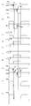
- Fig. 4 shows the operation time chart. However, the time chart of FIG. 4 and the following description are described on the assumption that an abnormality has occurred in the light emitting element 8a.
- An abnormality of the light emitting element 8a is detected.
- the light emitting element 8a becomes abnormal, there are many cases where a short circuit is mainly caused. Therefore, the voltage applied to the light emitting element 8a decreases.
- Vla and Vla1 are lowered.
- the light emitting element voltage detection circuit 12 detects that Vla and Vla1 have decreased, and sends a signal to the microcomputer 16.
- the conditions for detecting that an abnormality has occurred in the light emitting element 8a are as follows: i) If Vla drops below Vth1, ii) When Vla1 drops below Vth3, iii) If both i) and ii) are met, Any of the above three conditions may be used.
- the light emitting element 8a in which an abnormality has occurred is specified.
- a normal light emitting element if a constant current flows, the voltage applied to both ends of the light emitting element does not change.
- the microcomputer 16 since the voltage Vla1 applied to the light emitting element 8a is decreased, the microcomputer 16 determines that an abnormality has occurred in the light emitting element 8a based on a signal sent from the light emitting element voltage detection circuit 12. To do.
- the light emitting element 8a in which an abnormality occurred in step (2) was identified.
- the normal light emitting elements 8b and 8c do not flow current even when a voltage is applied in the reverse direction, and the abnormal light emitting element 8a has a characteristic of flowing when a voltage is applied in the reverse direction.
- the microcomputer 16 inputs a gate signal to the FETs (Q8, Q9) connected in parallel to the normal light emitting elements 8b, 8c.
- the microcomputer 16 since an abnormality has occurred in the light emitting element 8a, the microcomputer 16 inputs a signal to the drive IC3 (15), inputs a gate signal to the switching elements Q8 and Q9, and turns on the light emitting elements 8b and 8c. Short circuit. At the same time, the switching elements Q3 and Q6 are turned off and the switching elements Q4 and Q5 are turned on to apply a reverse voltage to the light emitting element 8a.
- Vla decreases to ⁇ Vin (Vin is a voltage between the step-down chopper output voltage C2).
- the light emitting element voltage detection circuit 12 detects that Vla has dropped and sends a signal to the microcomputer 16.
- Vla1 decreases to ⁇ Vin.
- the short circuit state is shifted to the open state, the current value Ila flowing through the light emitting element 8a increases.
- the light emitting element current detection circuit 11 detects that Ila has risen and sends a signal to the microcomputer 16.
- the conditions for detecting that the light emitting element 8a has returned are as follows (see FIG. 4): i) If Vla drops below Vth2, ii) When Vla1 drops below Vth4 ii) If Ila rises above Ith1, iv) If two of i), ii) and iii) are met, v) If all three of i), ii) and iii) are met, Any of the above five conditions may be used.
- a normal current is passed through the light emitting element 8a.
- the microcomputer 16 sends a signal to the drive ICs 1, 2 (13, 14), turns on the switching elements Q3, Q6, and turns on the switching element Q4. , Q5 is turned off.
- the microcomputer 16 inputs the gate signal to the switching elements Q8 and Q9 in step (3), but stops the signal. Therefore, a current flows through the light emitting elements 8b and 8c in the same direction as normal, and the light emitting elements 8a, 8b and 8c emit light.
- the forward / reverse inverting circuit 6 assigned to the light emitting elements 8a, 8b, 8c and the short-circuit switches Q7, Q8, provided for each of the light emitting elements 8a, 8b, 8c, Q9 the reverse voltage is surely applied to the abnormal light emitting element 8a, while the reverse voltage can be avoided to be applied to the normal light emitting elements 8b and 8c, and the abnormal light emitting element 8a is recovered. be able to.
- the short-circuit switches Q7, Q8, and Q9 are composed of field effect transistors (FETs) that can operate at high speed, it is possible to avoid applying a reverse voltage to the normal light-emitting elements 8b and 8c at high speed, and normal light emission. It is possible to avoid applying stress to the elements 8b and 8c.
- FETs field effect transistors
- FIG. 5 is a diagram for explaining the configuration of the light emitting device 100 according to the third embodiment of the present invention.
- Vla is a voltage applied to the entire light emitting elements 8a, 8b and 8c
- Vla1 is a voltage applied to the light emitting element 8a
- Vla2 is a voltage applied to the light emitting element 8b
- Vla3 is applied to the light emitting element 8c.
- Voltage. Ila is a current flowing through the light emitting elements 8a, 8b, and 8c.
- the light emitting elements 8a, 8b, and 8c are organic electroluminescent panels, and each light emitting element 8a, 8b, and 8c has a pair of an anode and a cathode.
- the forward / reverse inversion circuit 6 includes an abnormal short circuit 9a including resistors R11, R12, R13, a capacitor C11, and a thyristor D11 in each light emitting element 8a, 8b, 8c, resistors R14, R15, R16, a capacitor C12, and a thyristor D12.
- the abnormal short circuit 9b, the resistors R17, R18, R19, the capacitor C13, and the thyristor D13 that are configured are connected in parallel one by one. (See FIGS. 5 and 8.
- FIG. 8 is an enlarged view of the main part of FIG. 5.)
- the main flow of operation is (1) An abnormality of the light emitting element 8a is detected. (2) A reverse voltage is applied to the light emitting element 8a. A current flows in the opposite direction to the light emitting element 8a in which an abnormality has occurred (refresh current), and the other normal elements 8b and 8c are operated by the abnormal short circuits 9b and 9c connected in parallel to the elements 8b and 8c. Thus, short-circuiting is performed so that a reverse voltage is not applied to each of the normal light emitting elements 8b and 8c. (3) It is detected that the light emitting element 8a in which an abnormality has occurred has returned to normal. (4) A normal current is passed through the light emitting elements 8a, 8b, 8c.
- Fig. 6 shows the operation time chart. However, the time chart of FIG. 6 and the following description are described on the assumption that an abnormality has occurred in the light emitting element 8a.
- An abnormality of the light emitting element 8a is detected (T1).
- T1 An abnormality of the light emitting element 8a is detected.
- the light emitting element 8a becomes abnormal, there are many cases where a short circuit is mainly caused. Therefore, the voltage applied to the light emitting element 8a decreases.
- Vla and Vla1 are lowered.
- the light emitting element voltage detection circuit 12 detects that Vla and Vla1 have decreased, and sends a signal to the microcomputer 16.
- the conditions for detecting that an abnormality has occurred in the light emitting element 8a are as follows: i) If Vla drops below Vth1, ii) When Vla1 drops below Vth4 iii) If both i) and ii) are met, Any of the above three conditions may be used.
- the microcomputer 16 When the abnormality of the light emitting element 8a is detected in step (1), the microcomputer 16 inputs a signal to the drive ICs 1, 2 (13, 14), turns off the switching elements Q3, Q6, and turns on the switching elements Q4, Q5 to emit light. A reverse voltage is applied to the element 8a.
- the normal light emitting elements 8b and 8c do not flow current even when a voltage is applied in the reverse direction, and the light emitting element 8a in which an abnormality has occurred has a characteristic of flowing when a voltage is applied in the reverse direction. Since an abnormality has occurred in the light emitting element 8a, the current path that flows when the switching elements Q3 and Q6 are turned off and the switching elements Q4 and Q5 are turned on is as follows: switching element Q4 ⁇ abnormal short circuit 9c ⁇ abnormal short circuit 9b ⁇ light emitting element 8a ⁇ Current flows in the order of switching element Q5.
- the abnormal short circuit 9c will be described as an example.
- the switching elements Q3 and Q6 of the forward / reverse inverting circuit 6 in FIG. 5 are turned off and the switching elements Q4 and Q5 are turned on, first, current flows in the order of R17 ⁇ C13 and R18. Therefore, the voltage between C13 rises. Since a voltage is applied to the thyristor D13 so that a forward current flows between the anode and the cathode, the thyristor D13 is turned on when the voltage across the C13 exceeds a certain value.
- D12 is turned on by the same principle, so that the normal light emitting elements 9b and 9c are short-circuited. From the above, when switching elements Q3 and Q6 are turned off, switching elements Q4 and Q5 are turned on and a reverse voltage is applied to light emitting element 8a, no voltage is applied to normal light emitting elements 8b and 8c, and abnormal light emission occurs. A voltage is applied to the element 8a and a current flows in the opposite direction.
- the conditions for detecting that the light emitting element 8a is restored by the light emitting element voltage detection circuit 12 and the light emitting element current detection circuit 11 are as follows. When the light emitting element 8a is restored and the thyristor D11 is not yet turned on,
- a normal current is passed through the light emitting element 8a (T4).
- the microcomputer 16 sends a signal to the drive ICs 1, 2 (13, 14), turns on the switching elements Q3, Q6, and turns on the switching element Q4. , Control to turn off Q5.
- a current flows through the light emitting elements 8a, 8b, and 8c in the same direction as normal, and the light emitting elements 8a, 8b, and 8c emit light.
- the forward / reverse inverting circuit 6 assigned to the light emitting elements 8a, 8b, 8c and the abnormal short circuit 9a, 9b provided for each of the light emitting elements 8a, 8b, 8c. 9c it is possible to reliably apply a reverse voltage to the abnormal light emitting element 8a, while avoiding applying a reverse voltage to the normal light emitting elements 8b and 8c, and to recover the abnormal light emitting element 8a. Can be made.
- the thyristors D12, 13 are automatically turned on to protect the normal light emitting elements 8b, 8c, so that the thyristors D11, 12, 13 are driven. For this reason, the drive IC is not required, and the configuration of the light emitting device 100 can be simplified.
- FIG. 7 is a diagram for explaining a schematic configuration of a lighting fixture 200 using organic electroluminescence used in the embodiment of the present invention.
- the luminaire 200 includes a light emitting element 32 and a light emitting element 32 sandwiched between an organic light emitting layer 29 and a transparent electrode ITO 28 that supplies power thereto, an aluminum electrode 30, and glasses 27 and 31 for protecting the organic light emitting layer 29.
- An electronic component 23 for supplying power and a printed circuit board 24 are included and housed in a case 22.
- Reference numeral 21 denotes a light emitting surface, 25 denotes a case upper surface, and 26 denotes a case lower surface.
- the lighting circuit including the forward / reverse inversion circuit of the light emitting device described in the first to third embodiments includes a power supply unit (not shown) for supplying power, an electronic component 23, and a printed board 24.
- the said embodiment demonstrated the case where an organic electroluminescent element was used as a light emitting element, it is not limited to an organic electroluminescent element, An inorganic electroluminescent element, LED, etc. electrodes Needless to say, the present invention can be applied to other elements that can be refreshed by repairing a defective insulation portion in an element that emits light by applying a voltage therebetween.
- the lighting fixture was demonstrated in the said embodiment, it cannot be overemphasized that it is applicable to various light sources, such as a light source for exposure, without being limited to a lighting fixture.
- the present invention can apply an inverse voltage to an abnormal light-emitting element to allow a refresh current to flow, thereby recovering the abnormal light-emitting element and avoiding stress on the normal light-emitting element. It can be used as a luminescent light emitting device and a lighting fixture.
Landscapes
- Physics & Mathematics (AREA)
- Optics & Photonics (AREA)
- Electroluminescent Light Sources (AREA)
- Devices For Indicating Variable Information By Combining Individual Elements (AREA)
Abstract
Description
また、有機エレクトロルミネッセント素子に所望の直流電圧を供給する直流電源手段と、直流電源手段の電圧供給の停止を検出する検出手段と、直流電源手段の電圧供給が停止されたときに有機エレクトロルミネッセント素子に逆特性の電圧を供給する逆電圧供給手段とを具備した照明装置も提案されている(特許文献3)。
一方、特許文献3においては、直流電源手段の電圧供給の停止が検出されたときに有機エレクトロルミネッセント素子に逆特性の電圧を供給するようにしているため、この場合も、別途リフレッシュのための時間を設ける必要がある。
また、リフレッシュ不要なエレクトロルミネッセント素子に逆電圧をかけても点灯できないだけでなく、ストレスがかかることになる。
2 PFC回路
3 PFC制御回路
4 降圧チョッパ回路
5 降圧チョッパ制御回路
6 順逆反転回路
7 発光素子電圧・電流制御回路
8、8a、8b、8c、32 発光素子
9a、9b、9c 異常短絡回路
11 発光素子電流検知回路
12 発光素子電圧検知回路
13、14、15 ドライブIC
16 マイコン
21 発光面
22 ケース
23 電子部品
24 プリント基板
25 ケース上
26 ケース下
27、31 ガラス
28 ITO
29 有機発光層
30 アルミ電極
100 発光装置
200 照明器具
図1は、本発明の実施の形態にかかる発光装置100の構成を説明するための図である。本実施の形態の発光装置100は、AC電源1を整流するダイオード・ブリッジDBから直流電力が供給される力率改善回路2(以下、PFC(Power Factor Correction)回路2という)と、PFC回路2の出力電圧を発光素子に供給する電圧に変換する降圧チョッパ回路4と、発光素子8に供給する電流を切り替える順逆反転回路6と、発光素子電流検知回路11、発光素子電圧検知回路12、ドライブIC13、14およびマイコン16を含み、発光素子8の電圧および電流を制御する発光素子電圧・電流制御回路7とを有する。
(1)発光素子8の異常を検知する。
(2)発光素子8に通常と逆向きの電圧を印加する。
(3)発光素子8が正常に復帰したことを検知する。
(4)発光素子8に通常の電流を流す、である。
(1)発光素子8の異常を検知する(T1)。
発光素子8が異常になる場合、主に短絡になるケースが多い。そのためVla(発光素子に印加される電圧)が低下する。発光素子電圧検知回路12によりVlaが低下したこと
を検知し、マイコン16に信号を送る。
VlaがVth1まで低下するとマイコン16がドライブIC1、2(13、14)に信号を送り、スイッチング素子Q3、Q6をオフしてスイッチング素子Q4、Q5をオンする。そのため発光素子8に通常とは逆向きの電圧が印加される。このとき、発光素子8には逆向きの電流(リフレッシュ電流)が流れる。
発光素子8が復帰すると、短絡状態から開放状態に移る。そのためVlaが-Vin(Vinは降圧チョッパ出力電圧C2間電圧)まで低下する。発光素子電圧検知回路12によりVlaが低下したことを検知しマイコン16に信号を送る。また、短絡状態から開放状態に移るため、発光素子8に流れる電流値Ilaが上昇する。発光素子電流検知回路11によりIlaが上昇したことを検知しマイコン16に信号を送る。
i) VlaがVth2以下に低下した場合、
ii) IlaがIth1以上に上昇した場合、
iii)i)、ii) 両方を満たした場合、
以上3つのうちどの条件でもよい。
VlaがVth2まで低下する(IlaがIth1以上になる)と、マイコン16がドライブIC1、2(13、14)に信号を送り、スイッチング素子Q3、Q6をオンしてスイッチング素子Q4、Q5をオフする。そのため発光素子8に通常時と同じ向きに電流が流れて発光素子8が発光する。
図3は、本発明の実施の形態2にかかる発光装置100の構成を説明するための図である。同図のVlaは発光素子8a、8b、8c全体に印加される電圧、Vla1は発光素子8aに印加される電圧、Vla2は発光素子8bに印加される電圧、Vla3は発光素子8cに印加される電圧である。また、Ilaは発光素子8a、8b、8cに流れる電流である。
(1)発光素子8aの異常を検知する。
(2)異常が発生した発光素子8aを特定する。
(3)異常が発生した発光素子8aに通常と逆向きの電圧を印加する。それ以外の正常な素子8b、8cは、各素子8b、8cに並列に接続されているFETQ8、Q9をオンにして、正常な各々の発光素子8b、8cに逆電圧が印加されないよう制御する。
(4)異常が発生した発光素子8aが正常に復帰したことを検知する。
(5)発光素子8a、(8b、8c)に通常の電流を流す。
発光素子8aが異常になる場合、主に短絡になるケースが多い。そのため発光素子8aに印加される電圧が低下する。実施の形態2では、発光素子8aに異常が発生しているので、Vla、Vla1が低下する。発光素子電圧検知回路12によりVla、Vla1が低下したことを検知し、マイコン16に信号を送る。
i) VlaがVth1以下に低下した場合、
ii) Vla1がVth3以下に低下した場合、
iii) i)、ii) 両方とも満たした場合、
以上の3つのうちどの条件でもよい。
正常な発光素子の場合、一定電流が流れていれば発光素子両端に印加される電圧に変化がない。実施の形態2の場合、発光素子8aに印加される電圧Vla1が低下しているので、発光素子電圧検知回路12から送られて来る信号により、発光素子8aに異常が発生したとマイコン16が判別する。
るので、異常が発生したパネルのみ逆向きに電流(リフレッシュ電流)を流し、その他の正常な発光素子8b、8cに逆向きに電圧を印加しない。
発光素子8aが復帰すると、短絡状態から開放状態に移る。そのためVlaが-Vin(Vinは降圧チョッパ出力電圧C2間電圧)まで低下する。発光素子電圧検知回路12によりVlaが低下したことを検知してマイコン16に信号を送る。Vla1も同様に-Vinまで低下する。また、短絡状態から開放状態に移るため、発光素子8aに流れる電流値Ilaが上昇する。発光素子電流検知回路11によりIlaが上昇したことを検知しマイコン16に信号を送る。
i) VlaがVth2以下に低下した場合、
ii) Vla1がVth4以下に低下した場合、
ii) IlaがIth1以上に上昇した場合、
iv) i)、ii)、iii) のうち2つ満たした場合、
v) i)、ii)、iii) のうち3つとも全て満たした場合、
以上5つのうちどの条件でもよい。
ステップ(4)に記載したi)~v) のいずれかの条件を満たすと、マイコン16がドライブIC1、2(13、14)に信号を送り、スイッチング素子Q3、Q6をオンしてスイッチング素子Q4、Q5をオフする。また、マイコン16はステップ(3)でスイッチング素子Q8、Q9にゲート信号を入力していたが、その信号を停止する。そのため発光素子8b、8cに通常時と同じ向きに電流が流れて発光素子8a、8b、8cが発光する。
図5は、本発明の実施の形態3にかかる発光装置100の構成を説明するための図である。同図のVlaは発光素子8a、8b、8c全体に印加される電圧、Vla1は発光素子8aに印加される電圧、Vla2は発光素子8bに印加される電圧、Vla3は発光素子8cに印加される電圧である。また、Ilaは発光素子8a、8b、8cに流れる電流で
ある。実施の形態1と同様に、発光素子8a、8b、8cは有機エレクトロルミネッセントパネルであり、各発光素子8a、8b、8cは陽極と陰極を1対ずつ有している。
(1)発光素子8aの異常を検知する。
(2)発光素子8aに通常と逆向きの電圧を印加する。異常が発生した発光素子8aに逆向きに電流が流れ(リフレッシュ電流)、それ以外の正常な素子8b、8cは各素子8b、8cに並列に接続されている異常短絡回路9b、9cが作動して、正常な各々の発光素子8b、8cに逆電圧が印加されないよう短絡する。
(3)異常が発生した発光素子8aが正常に復帰したことを検知する。
(4)発光素子8a、8b、8cに通常の電流を流す。
発光素子8aが異常になる場合、主に短絡になるケースが多い。そのため発光素子8aに印加される電圧が低下する。実施の形態3では、発光素子8aに異常が発生しているので、Vla、Vla1が低下する。発光素子電圧検知回路12によりVla、Vla1が低下したことを検知し、マイコン16に信号を送る。
i) VlaがVth1以下に低下した場合、
ii) Vla1がVth4以下に低下した場合、
iii) i)、ii)両方とも満たした場合、
以上の3つのうちどの条件でもよい。
素子Q4、Q5がオンした状態では、まず初めに電流はR17→C13、R18の順で流れる。そのためC13間電圧は上昇する。サイリスタD13にはアノードからカソード間に順方向電流が流れるように電圧が印加されているのでC13間の電圧がある値以上になると、サイリスタD13がオンする。
発光素子8aが復帰すると、短絡状態から開放状態に移る。そのため逆向きの電流は発光素子8aには流れず異常短絡回路9aに流れる。このときVla、Vla1は低下し、Ilaは上昇する。この間、異常短絡回路9aに電流が流れR11を介してC11間電圧が上昇する。C11間電圧がVth3以上になるとサイリスタD11がオンするため、VlaVla1が上昇してIlaが低下する。
ii) Vla1がVth5以下に低下した場合、
ii) IlaがIth1以上に上昇した場合、
iv) i)、ii)、iii) のうち2つ満たした場合、
v) i)、ii)、iii) のうち3つとも全て満たした場合、
vi) VlaがVth2以上に上昇した場合、
vii) Vla1がVth5以上に上昇した場合、
viii) IlaがIth1以下に低下した場合、
ix) vi)、vii)、viii) のうち2つ満たした場合、
x) vi)、vii)、viii) のうち3つとも全て満たした場合、
以上のi)~x) のうちどの条件でもよい。
ステップ(3)に記載したi)~x) のいずれかの条件を満たすと、マイコン16がドライブIC1、2(13、14)に信号を送り、スイッチング素子Q3、Q6をオンしてスイッチング素子Q4、Q5をオフするように制御する。発光素子8a、8b、8cに通常時と同じ向きに電流が流れて発光素子8a、8b、8cが発光する。
図7は、本発明の実施の形態で用いられる有機エレクトロルミネッセントを用いた照明器具200の概略構成を説明するための図である。照明器具200は有機発光層29とそれに電力を供給する透光性電極ITO28、アルミ電極30、有機発光層29を保護するためのガラス27、31で挟まれている発光素子32と発光素子32に電力を供給する電子部品23、プリント基板24を含み、ケース22に収納されている。21は発光面、25はケース上面、26はケース下面を示す。また、前記実施の形態1乃至3で説明した発光装置の順逆反転回路を含む点灯回路は電力を供給する給電部(図示省略)と電子部品23とプリント基板24で構成される。
なお、前記実施の形態では、発光素子として有機エレクトロルミネッセント素子を用いた場合について説明したが、有機エレクトロルミネッセント素子に限定されることなく、無機エレクトロルミネッセント素子、LEDなど、電極間に電圧を印加することによって発光する素子などにおいて、絶縁不良部を修復することで、リフレッシュできる他の素子にも適用可能であることはいうまでもない。
また、前記実施の形態では、照明器具について説明したが、照明器具に限定されることなく、露光用光源などの各種光源に適用可能であることはいうまでもない。
Claims (5)
- 直流電流の供給を受けて発光する複数の発光素子と、
発光素子に一定以上の電流を供給する直流電源回路と、
前記発光素子に印加される電圧を検知する発光素子電圧検知回路と、
前記発光素子電圧検知回路が前記発光素子の異常を検知した場合に、異常を検知した発光素子に逆方向電圧を印加する順逆反転回路とを備えた発光装置。 - 請求項1記載の発光装置であって、
前記順逆反転回路は、異常を検知した発光素子に逆方向電圧を印加する場合に、正常な発光素子を短絡する短絡スイッチを備えた発光装置。 - 請求項1記載の発光装置であって、
前記複数の発光素子は、直列に接続され、
前記短絡スイッチは、前記複数の発光素子のおのおのに並列に接続され、
前記発光素子電圧検知回路は、前記複数の発光素子のおのおのに印加される電圧を検知し、電圧値の変化により発光素子の異常を検知する発光装置。 - 請求項1記載の発光装置であって、
前記順逆反転回路は、前記発光素子に流れる電流を検知する発光素子電流検知回路を備える発光装置。 - 請求項1または2記載の発光装置であって、
前記順逆反転回路は、電源間に直列接続され、その直列接続点が前記単数または複数の発光素子の一端に接続される第1および第2のスイッチング素子と、
前記電源間に直列接続され、その直列接続点が前記単数または複数の発光素子の他端に接続される第3および第4のスイッチング素子とを有し、
前記第2および第3のスイッチング素子が導通して異常を検知した発光素子に逆方向電圧を印加してリフレッシュし、前記第1および第4のスイッチング素子が導通してリフレッシュした発光素子に順方向電圧を印加する発光装置。
Priority Applications (3)
| Application Number | Priority Date | Filing Date | Title |
|---|---|---|---|
| US12/934,720 US8513898B2 (en) | 2008-03-26 | 2009-03-26 | Light emitting device that restores abnormal light emitting element |
| EP09724406.5A EP2257122B1 (en) | 2008-03-26 | 2009-03-26 | Light emitting device |
| CN2009801107728A CN101982013B (zh) | 2008-03-26 | 2009-03-26 | 发光装置 |
Applications Claiming Priority (2)
| Application Number | Priority Date | Filing Date | Title |
|---|---|---|---|
| JP2008080241A JP5317325B2 (ja) | 2008-03-26 | 2008-03-26 | 発光装置 |
| JP2008-080241 | 2008-03-26 |
Publications (1)
| Publication Number | Publication Date |
|---|---|
| WO2009119773A1 true WO2009119773A1 (ja) | 2009-10-01 |
Family
ID=41113960
Family Applications (1)
| Application Number | Title | Priority Date | Filing Date |
|---|---|---|---|
| PCT/JP2009/056195 Ceased WO2009119773A1 (ja) | 2008-03-26 | 2009-03-26 | 発光装置 |
Country Status (5)
| Country | Link |
|---|---|
| US (1) | US8513898B2 (ja) |
| EP (1) | EP2257122B1 (ja) |
| JP (1) | JP5317325B2 (ja) |
| CN (1) | CN101982013B (ja) |
| WO (1) | WO2009119773A1 (ja) |
Cited By (1)
| Publication number | Priority date | Publication date | Assignee | Title |
|---|---|---|---|---|
| JP2013003024A (ja) * | 2011-06-17 | 2013-01-07 | Sharp Corp | リペア装置およびリペア方法、デバイスの製造方法 |
Families Citing this family (11)
| Publication number | Priority date | Publication date | Assignee | Title |
|---|---|---|---|---|
| JP4852660B2 (ja) | 2008-12-18 | 2012-01-11 | パナソニック株式会社 | 有機エレクトロルミネッセンス表示装置及びその製造方法 |
| JP5177709B2 (ja) | 2009-10-15 | 2013-04-10 | 株式会社デンソー | 電子制御装置 |
| JP5177710B2 (ja) | 2009-10-15 | 2013-04-10 | 株式会社デンソー | 電子制御装置 |
| DE102009052836A1 (de) * | 2009-11-13 | 2011-05-19 | Schott Ag | Schaltungsanordnung für eine LED-Lichtquelle |
| JP5566151B2 (ja) * | 2010-03-26 | 2014-08-06 | パナソニック株式会社 | 発光素子点灯装置及びこれを用いた灯具並びに照明器具 |
| JP5912466B2 (ja) * | 2010-12-10 | 2016-04-27 | 株式会社半導体エネルギー研究所 | 発光素子の駆動方法 |
| JP5842129B2 (ja) * | 2011-07-26 | 2016-01-13 | パナソニックIpマネジメント株式会社 | Led点灯装置及びそれを用いた照明器具 |
| JP5884026B2 (ja) * | 2011-08-05 | 2016-03-15 | パナソニックIpマネジメント株式会社 | 電源装置 |
| EP2610844B1 (en) | 2011-12-28 | 2019-07-31 | Samsung Electronics Co., Ltd. | Power supplying apparatus, power supplying method, organic light-emitting diode display apparatus |
| DE102013113261B4 (de) * | 2013-11-29 | 2023-06-22 | Pictiva Displays International Limited | Verfahren zum Betrieb eines organischen optoelektronischen Bauelements |
| RU2668946C2 (ru) * | 2014-01-28 | 2018-10-05 | Конинклейке Филипс Н.В. | Электролюминесцентное устройство со схемой обнаружения короткого замыкания |
Citations (11)
| Publication number | Priority date | Publication date | Assignee | Title |
|---|---|---|---|---|
| JPH03110786A (ja) * | 1989-09-25 | 1991-05-10 | Minolta Camera Co Ltd | 有機エレクトロルミネセンス装置 |
| JP2000348861A (ja) * | 1999-06-02 | 2000-12-15 | Toyota Central Res & Dev Lab Inc | 有機elディスプレイの評価装置 |
| JP2001117534A (ja) * | 1999-10-21 | 2001-04-27 | Pioneer Electronic Corp | アクティブマトリクス型表示装置及びその駆動方法 |
| JP2003229262A (ja) * | 2002-01-31 | 2003-08-15 | Toyota Industries Corp | 有機el表示パネルの短絡画素検査方法及びその装置 |
| JP2003234187A (ja) * | 2001-12-06 | 2003-08-22 | Fuji Electric Co Ltd | パッシブマトリクス有機薄膜発光ディスプレイおよびその修復方法 |
| JP2004070057A (ja) * | 2002-08-07 | 2004-03-04 | Tohoku Pioneer Corp | 発光表示パネルの駆動装置および駆動方法 |
| JP2005078828A (ja) * | 2003-08-28 | 2005-03-24 | Konica Minolta Holdings Inc | 照明装置および照明装置の駆動方法 |
| JP2007042492A (ja) * | 2005-08-04 | 2007-02-15 | Aitesu:Kk | 有機elリペア方法とリペア装置 |
| JP2007149463A (ja) | 2005-11-25 | 2007-06-14 | Matsushita Electric Works Ltd | 点灯装置及び照明装置 |
| JP2007200662A (ja) | 2006-01-25 | 2007-08-09 | Optrex Corp | 有機led素子の製造方法 |
| JP2007207703A (ja) | 2006-02-06 | 2007-08-16 | Sharp Corp | 有機エレクトロルミネッセンス装置の修復方法 |
Family Cites Families (10)
| Publication number | Priority date | Publication date | Assignee | Title |
|---|---|---|---|---|
| EP0974140A2 (en) * | 1998-02-06 | 2000-01-26 | Koninklijke Philips Electronics N.V. | Organic electroluminescent device |
| DE60142295D1 (de) * | 2000-07-28 | 2010-07-15 | Nichia Corp | Anzeigesteuerschaltung und anzeigevorrichtung |
| TW530427B (en) * | 2000-10-10 | 2003-05-01 | Semiconductor Energy Lab | Method of fabricating and/or repairing a light emitting device |
| JP3854173B2 (ja) * | 2002-02-27 | 2006-12-06 | 東北パイオニア株式会社 | 発光表示パネルの駆動方法および有機el表示装置 |
| US6809481B2 (en) * | 2002-02-28 | 2004-10-26 | Semiconductor Energy Laboratory Co., Ltd. | Light emitting device and electric device using the same |
| WO2006037363A1 (de) * | 2004-10-06 | 2006-04-13 | Fraunhofer-Gesellschaft zur Förderung der angewandten Forschung e.V. | Vorrichtung und verfahren zum ansteuern einer organischen leuchtdiode |
| US7911463B2 (en) * | 2005-08-31 | 2011-03-22 | O2Micro International Limited | Power supply topologies for inverter operations and power factor correction operations |
| JP4887757B2 (ja) * | 2005-11-25 | 2012-02-29 | パナソニック電工株式会社 | 点灯装置及び照明装置 |
| JP2007200610A (ja) * | 2006-01-24 | 2007-08-09 | Koito Mfg Co Ltd | 車両用灯具の点灯制御装置 |
| JP5219255B2 (ja) * | 2008-03-26 | 2013-06-26 | パナソニック株式会社 | 発光装置 |
-
2008
- 2008-03-26 JP JP2008080241A patent/JP5317325B2/ja not_active Expired - Fee Related
-
2009
- 2009-03-26 EP EP09724406.5A patent/EP2257122B1/en not_active Not-in-force
- 2009-03-26 WO PCT/JP2009/056195 patent/WO2009119773A1/ja not_active Ceased
- 2009-03-26 CN CN2009801107728A patent/CN101982013B/zh not_active Expired - Fee Related
- 2009-03-26 US US12/934,720 patent/US8513898B2/en active Active
Patent Citations (11)
| Publication number | Priority date | Publication date | Assignee | Title |
|---|---|---|---|---|
| JPH03110786A (ja) * | 1989-09-25 | 1991-05-10 | Minolta Camera Co Ltd | 有機エレクトロルミネセンス装置 |
| JP2000348861A (ja) * | 1999-06-02 | 2000-12-15 | Toyota Central Res & Dev Lab Inc | 有機elディスプレイの評価装置 |
| JP2001117534A (ja) * | 1999-10-21 | 2001-04-27 | Pioneer Electronic Corp | アクティブマトリクス型表示装置及びその駆動方法 |
| JP2003234187A (ja) * | 2001-12-06 | 2003-08-22 | Fuji Electric Co Ltd | パッシブマトリクス有機薄膜発光ディスプレイおよびその修復方法 |
| JP2003229262A (ja) * | 2002-01-31 | 2003-08-15 | Toyota Industries Corp | 有機el表示パネルの短絡画素検査方法及びその装置 |
| JP2004070057A (ja) * | 2002-08-07 | 2004-03-04 | Tohoku Pioneer Corp | 発光表示パネルの駆動装置および駆動方法 |
| JP2005078828A (ja) * | 2003-08-28 | 2005-03-24 | Konica Minolta Holdings Inc | 照明装置および照明装置の駆動方法 |
| JP2007042492A (ja) * | 2005-08-04 | 2007-02-15 | Aitesu:Kk | 有機elリペア方法とリペア装置 |
| JP2007149463A (ja) | 2005-11-25 | 2007-06-14 | Matsushita Electric Works Ltd | 点灯装置及び照明装置 |
| JP2007200662A (ja) | 2006-01-25 | 2007-08-09 | Optrex Corp | 有機led素子の製造方法 |
| JP2007207703A (ja) | 2006-02-06 | 2007-08-16 | Sharp Corp | 有機エレクトロルミネッセンス装置の修復方法 |
Non-Patent Citations (1)
| Title |
|---|
| See also references of EP2257122A4 |
Cited By (1)
| Publication number | Priority date | Publication date | Assignee | Title |
|---|---|---|---|---|
| JP2013003024A (ja) * | 2011-06-17 | 2013-01-07 | Sharp Corp | リペア装置およびリペア方法、デバイスの製造方法 |
Also Published As
| Publication number | Publication date |
|---|---|
| JP5317325B2 (ja) | 2013-10-16 |
| US20110101875A1 (en) | 2011-05-05 |
| JP2009238435A (ja) | 2009-10-15 |
| EP2257122B1 (en) | 2017-01-11 |
| EP2257122A1 (en) | 2010-12-01 |
| US8513898B2 (en) | 2013-08-20 |
| EP2257122A4 (en) | 2014-11-05 |
| CN101982013A (zh) | 2011-02-23 |
| CN101982013B (zh) | 2013-03-06 |
Similar Documents
| Publication | Publication Date | Title |
|---|---|---|
| JP5317325B2 (ja) | 発光装置 | |
| JP5219255B2 (ja) | 発光装置 | |
| KR20100093220A (ko) | 유기전계발광 표시장치의 화소수리구조 및 그 수리방법 | |
| US9954202B2 (en) | Method for manufacturing electroluminescent display device | |
| JP2010032741A5 (ja) | ||
| JPH11162637A (ja) | 有機発光ダイオードの修復方法 | |
| CN106463643B (zh) | 有机发光装置 | |
| EP3113227B1 (en) | Organic light emitting display device | |
| JP5854212B2 (ja) | 発光装置及び有機el素子の駆動方法 | |
| KR20220019741A (ko) | 유기전계 발광소자 | |
| JP3633841B2 (ja) | 有機薄膜発光ディスプレイの修復方法 | |
| US9196875B2 (en) | Manufacturing method for organic EL lighting device | |
| US10777619B2 (en) | Organic EL device | |
| KR101938697B1 (ko) | 유기발광소자의 수리방법 | |
| JP6366088B2 (ja) | 有機el素子のリペア方法、有機elパネルの製造方法、及び発光装置 | |
| JP4207593B2 (ja) | 有機薄膜発光ディスプレイ | |
| JP5556594B2 (ja) | 照明装置 | |
| WO2015128921A1 (ja) | 表示装置の製造方法 | |
| JP7048246B2 (ja) | 発光システム | |
| JP2005241776A (ja) | 表示素子の製造、駆動方法 | |
| WO2019093492A1 (ja) | 発光部材、発光システム及び発光部材の製造方法 | |
| JP2016100171A (ja) | 有機エレクトロルミネッセンス表示装置の製造方法 | |
| WO2015059844A1 (ja) | 有機el表示装置の製造方法 | |
| JP2005258259A (ja) | 画像表示装置 |
Legal Events
| Date | Code | Title | Description |
|---|---|---|---|
| WWE | Wipo information: entry into national phase |
Ref document number: 200980110772.8 Country of ref document: CN |
|
| 121 | Ep: the epo has been informed by wipo that ep was designated in this application |
Ref document number: 09724406 Country of ref document: EP Kind code of ref document: A1 |
|
| REEP | Request for entry into the european phase |
Ref document number: 2009724406 Country of ref document: EP |
|
| WWE | Wipo information: entry into national phase |
Ref document number: 2009724406 Country of ref document: EP |
|
| NENP | Non-entry into the national phase |
Ref country code: DE |
|
| WWE | Wipo information: entry into national phase |
Ref document number: 12934720 Country of ref document: US |